
 Open Access Article
 This Open Access Article is licensed under a Creative Commons Attribution-Non Commercial 3.0 Unported Licence
Electrochemically reduced graphene oxide (ERGO)-Cu bilayer structure fabricated at room temperature for future interconnects†
Yuan Tian ,
Silin Han,
Peixin Chen,
Liang Cao,
Anmin Hu,
Ming Li and
Yunwen Wu*
,
Silin Han,
Peixin Chen,
Liang Cao,
Anmin Hu,
Ming Li and
Yunwen Wu*
State Key Laboratory of Metal Matrix Composites, School of Material Science and Engineering, Shanghai Jiao Tong University, No. 800 Dongchuan Road, Shanghai 200240, People's Republic of China. E-mail: tlwuyunwen@sjtu.edu.cn
First published on 16th January 2023
Abstract
Copper is an important interconnect material in integrated circuits (IC) due to its outstanding electrical and thermal properties. However, the development of the IC industry requires novel interconnect materials with higher conductivity. Here, uniform graphene oxide (GO) is deposited on copper by electrophoretic deposition (EPD) to obtain a GO-Cu bilayer structure at room temperature. (3-Mercaptopropyl) trimethoxysilane (MPTS) is self-assembled on the Cu anode surface, which protects the anode from oxidation during the EPD process. We find that the in situ hydrolysis of methoxy under the promotion of EPD voltage can facilitate the uniform deposition of GO and enhance the interface bonding force. In order to achieve better electrical performance, different reduction methods are conducted to reduce the structural disorder of GO. ERGO-Cu reduced by the electrochemical reduction method at −0.75 V for 1 min shows the lowest square resistance with a 16% resistance decrease compared with the GO-Cu structure and a 4.5% decrease compared with Cu substrate, due to the proper adjustment of the GO crystal structure. The room temperature fabricated ERGO-Cu bilayer structure provides a possibility for future interconnects with improved conductivity.
1 Introduction
From the Damascus technology to chip packaging, copper is the main interconnect material in the integrated circuit (IC) industry due to its outstanding electrical and thermal properties.1 For achieving better performance in electronic devices, new interconnect materials with improved conductivity are required to lower the resistance. Graphene, which is a two-dimensional array of sp2-bonded carbon atoms, is known to have extraordinary electrical and mechanical properties. The carrier mobility of graphene is 2.5 × 104 cm2 (V−1 s−1) and the maximum current-carrying capacity is up to 108 A cm−2.2,3 Therefore, graphene-based materials show great potential for future interconnect, such as composite made of copper and graphene,4 graphene-Cu bilayer structure,5 and pure graphene interconnect.6In these structures, graphene-Cu bilayer has been proposed to be highly conductive and therefore has an extensive interconnect application.8 Few-layers graphene can be deposited on the upper layer of the copper by chemical vapour deposition (CVD) to form a graphene-Cu bilayer interconnect structure.7 However, the devices in the IC cannot withstand the high preparation temperature of CVD. Great efforts have been made to solve this problem. Kang et al.7 prepared multi-layer graphene on Ni foil by CVD at 900 °C, and then transferred it to the surface of the target substrate to form the graphene-Cu bilayer interconnect structure. Yeh et al.8 used electron cyclotron resonance CVD to lower the preparation temperature of graphene-Cu bilayer interconnect to 400 °C. The deposited bilayer interconnect showed a ∼10% decrease in the resistivity of fine test lines. Furthermore, Li et al.9 used the inductively coupled plasma CVD to further reduce the preparation temperature of graphene-Cu structure to below 400 °C. This bilayer structure also exhibits low resistivity, half that of as-fabricated Cu wire. Nevertheless, realizing room temperature fabrication of graphene-Cu bilayer structure for IC application remains challenging.
Electrophoretic deposition (EPD) exhibits many advantages, such as high deposition rate, possibility of deposition on substrates of complex shape and capability of composite film formation.10 Stable graphene dispersion needed for EPD can be easily prepared by the Hummers' method (named GO colloidal).11 Graphene film formed by the EPD method has already been explored in some fields, such as corrosion resistance,12 lithium-ion battery electrodes,13 and supercapacitors.14 However, most of these works focused on improving the specific surface area and pay little attention to surface roughness, which is an important factor in reducing electrical resistance. In addition, there are also many lattice defects caused by the Hummers' etching process in the carbon skeleton of GO flakes. These two problems lead to a significant increase in the overall resistance of the graphene-Cu bilayers prepared by EPD.
Herein, we report a surface modification method to lower the surface roughness of GO-Cu fabricated by EPD method at room temperature. In addition, electrochemical reduction is used to reduce the GO film to further increase the conductivity of the fabricated GO-Cu structure. The (3-mercaptopropyl) trimethoxysilane (MPTS) molecules are selected to act as a modification layer to protect the Cu from being oxidized. In addition, the in situ hydrolysis of MPTS can form hydroxyl on the substrate surface. The chemical bond between the terminal group and the hydroxyl group in the GO sheets greatly enhances the bonding force of graphene-Cu and reduces the surface roughness by 25%. Finally, we study the impacts of electrochemical reduction, chemical reduction and low-temperature thermal reduction on the structure and resistivity of GO film under the consideration of IC manufacturing compatibility. After an electrochemical reduction process with adjustment of reduction condition, the square resistance of ERGO-Cu structure is reduced by 16% compared with original GO-Cu structure and 4.5% compared with Cu substrate.
2 Experimental section
2.1 Preparation
2.2 Characterization
Dynamic light scattering (DLS) measurement was performed on a Zetasizer (BIC Omni) to determine the zeta potential of synthesized GO in the solution. The surface morphology of the deposited sample was observed by scanning electron microscopy (SEM, MIRA3 TESCA). The X-ray photoelectron spectra (XPS) were obtained on Nexsa ThermoFisher scientific using a focused monochromatic aluminium Kα X-ray (1486.6 eV) source and a spherical section analyzer. The X-ray beam used was 150 W and the sample area was 300 μm × 700 μm. Wide-scan data were collected using a pass energy of 160 eV. The infrared spectrum was performed using iN10 MX (Thermo Fisher) and GO film was tested by ATR-FTIR (Zr single crystal). Raman spectrum was obtained with a confocal Raman microscope (Renishaw inVia Qontor, England). Materials were irradiated with light from a solid-state laser at 532 nm and the power of the excitation laser is 10 mW to avoid lase-induced heating. The surface roughness was measured by atomic force microscope (AFM, FastScan Bio Bruker America tip is AC240, 160). Contact angle test was performed by using diluted GO colloidal to detect the change of surface affinity by digital camera. Finally, the square resistance was measured by a multifunction digital four-probe tester (ST2258C, Suzhou Jingge, China). Detailed steps are listed in the ESI.†3 Results and discussion
Fig. 1a shows that the Raman spectrum of the prepared GO presented D and G bands centred at 1370 and 1583 cm−1 respectively. The defects of GO can be observed from the Raman spectrum, in which the ratio of the D and G band intensity (ID/IG, nearly 0.95) is an evaluation of the degree of crystal disordering.15 The average crystallite size of GO sheets is nearly 20 nm calculated by La = 2.4 × 10⁻¹⁰ × λ4 × (ID/IG)−1.16 The FTIR spectrum shown in Fig. 1b consists of oxygen-containing functional groups that include C![[double bond, length as m-dash]](https://www.rsc.org/images/entities/char_e001.gif) O (1711 cm−1), C–O–C (1050 cm−1) and O–H (3200–3500 cm−1). These functional groups give GO more properties than graphene such as hydrophilicity and water solubility.17 Fig. 1c is the SEM of GO sheets which clearly shows the intrinsic wrinkles of graphene oxide after drying. The zeta potential of GO dispersion is −49.2 mV, whose absolute value is much larger than 30 mV. This indicates that the as-prepared GO colloid has long-term stability.18 Tyndall effect shown in Fig. 1d can prove that GO disperses evenly in water and forms a stable colloid that can be used for EPD.
O (1711 cm−1), C–O–C (1050 cm−1) and O–H (3200–3500 cm−1). These functional groups give GO more properties than graphene such as hydrophilicity and water solubility.17 Fig. 1c is the SEM of GO sheets which clearly shows the intrinsic wrinkles of graphene oxide after drying. The zeta potential of GO dispersion is −49.2 mV, whose absolute value is much larger than 30 mV. This indicates that the as-prepared GO colloid has long-term stability.18 Tyndall effect shown in Fig. 1d can prove that GO disperses evenly in water and forms a stable colloid that can be used for EPD.
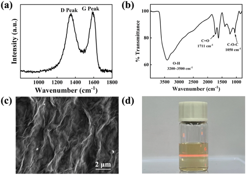 | ||
| Fig. 1 (a) Raman spectrum of pristine GO prepared by Hummers' method. (b) FTIR spectrum of pristine GO. (c) SEM of GO was diluted into 1 mg mL−1 and dropped on Si. (d) Tyndall effect of GO colloid. | ||
Copper is an easily oxidized metal, especially as an anode in the EPD process. Therefore, MPTS is self-assembled on the Cu surface as a protection layer. After MPTS was grafted onto copper substrates, the terminal group was easily in situ hydrolyzed to hydroxyl (–OH) in GO dispersion.19 The effects of MPTS layer can be concluded into two aspects as shown in Fig. 2a. Apart from protecting copper from being oxidized, the hydroxyl groups can react with GO sheets as shown in schematic detailly.20 The hydrolysis process of MPTS is confirmed by the change of contact angle after the water electrolyzed experiments in which the MPTS-modified surface state changes to hydrophilic from hydrophobic. In the S 2p XPS spectrum shown in Fig. 2b, the S 2p peak show four typical components: thiol bounds to Cu (Cu–S, 162.7 eV), unreacted –SH (164 eV), RSO32− (167.2 eV), RSO42− (168.4 eV) (data analysis according to ThermoFisher SCIENTIFIC, XPS full spectrum in ESI Fig. S2†). Fig. 2c and d present the surface morphology images of the specimens according to the anti-oxidization test in water by SEM and photographing methods. Without MPTS protection, large areas of dark red oxidation can be seen in the photos and many uneven oxides can be observed on the surface from the SEM. While under the protection of the MPTS modification layer, the formation of poorly conductive copper oxides can be avoided, and the quality of the graphene-Cu interface can be improved.
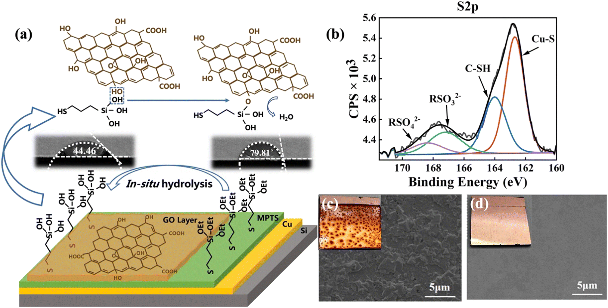 | ||
| Fig. 2 (a) Schematic illustration of the mechanism of MPTS facilitated GO deposition during EPD process. After the specimen was electrolyzed at 6 V for 5 min, the contact angle of MPTS surface changed from 79.81° to 44.46°. (b) XPS sulfur S 2p spectrum of MPTS-modified Cu. The observation of copper surface by SEM and optical microscope after conducting the water electrolyzed experiment at 6.0 V for 5 min (c) without (d) with the protection of MPTS. | ||
In addition, GO deposited by EPD can barely fully cover the Cu surface without MPTS modification due to the poor interface interaction between GO and Cu, as shown in Fig. 3a and b. The SEM of GO film deposited on Cu and MPTS-modified Cu surface after the adhesion tape test is shown in Fig. 3d and e, respectively. From the comparison of these two SEM images, GO film shows large area shedding without modification but exhibits the same morphology as the original sample with MPTS modification. The chemical bonding formed between MPTS-modified Cu surface and GO film can effectively improve the interface binding force.21 Therefore, GO film on MPTS-modified Cu has lower surface roughness and fewer wrinkles. From the AFM test shown in Fig. 3c, the roughness of GO film is decreased by 25% with the modification of MPTS. The increased roughness will cause exacerbated surface electron scattering, leading to poorer conductivity of GO film. In addition, the stacking of GO wrinkles is not conducive to the subsequent reduction process. The residual unreduced oxygen-containing functional groups will further decrease conductivity of GO film. Thus, combining the protection effect and in situ hydrolysis property of the assembled MPTS, improved binding force and flatness of deposited GO film can be achieved. We also explored the influence of EPD voltage on GO deposition. As the optical microscopies embedded in Fig. 3f shown, when the voltage was 4 V, large area of copper was uncovered. While the voltage was 8 V, GO sheets started to overlap unevenly and the thickness was too thick. Uniform and fully covered GO film could be deposited at 6 V with nearly 100 nm thickness.
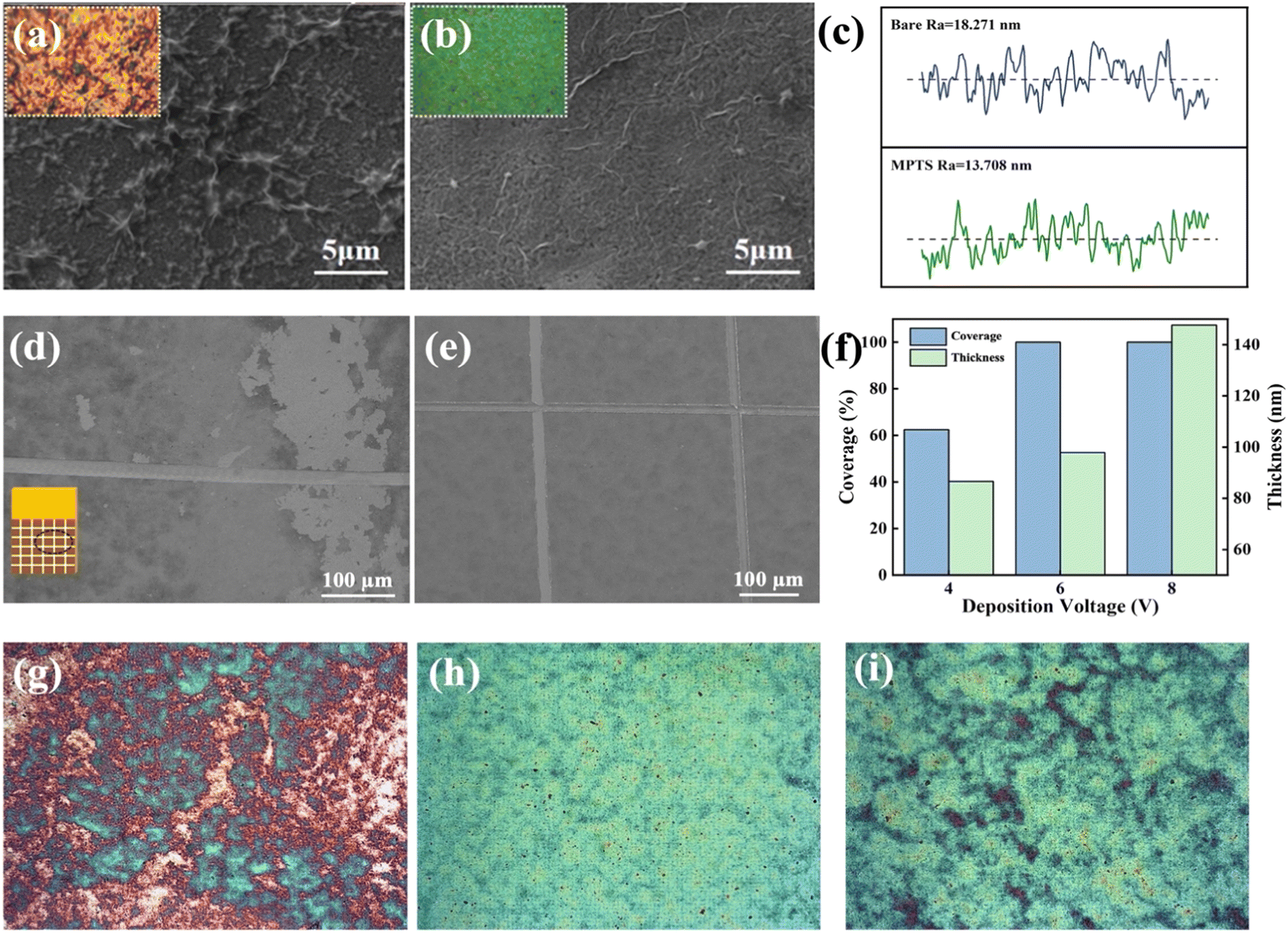 | ||
| Fig. 3 SEM of GO film microstructure deposited on (a) bare copper surface and (b) MPTS-modified copper surface at 6 V for 5 min. (c) AFM line scan of roughness of deposited GO film with or without MPTS modification (three-dimensional AFM images are shown in ESI Fig. S3†). (d) GO-Cu surface and (e) GO-MPTS-Cu surface after adhesion tape test. (f) Histogram of variation of coverage and thickness with deposition voltage. The thickness was tested by a step profiler (DektakXT, Bruker) and the coverage is calculated roughly by the GO and bare copper area ratio in optical microscopies. The optical microscopy (×1000) of GO film deposited at (g) 4 V, (h) 6 V, (i) 8 V. | ||
Fig. 4 shows the cross-sectional SEM images of the GO-Cu bilayer structure fabricated by EPD with the modification of MPTS at 6 V. As shown in Fig. 4a, GO film deposited on Cu shows a compact stacked structure with few wrinkles or swellings. From the other image shown in Fig. 4b, the layer-by-layer structure of GO can be observed clearly, and the thickness is estimated to be about 100 nm. The EDS mapping of C, Cu, and Si elements shown in Fig. 4d–f displays the sandwich structure of GO-Cu on Si wafer.
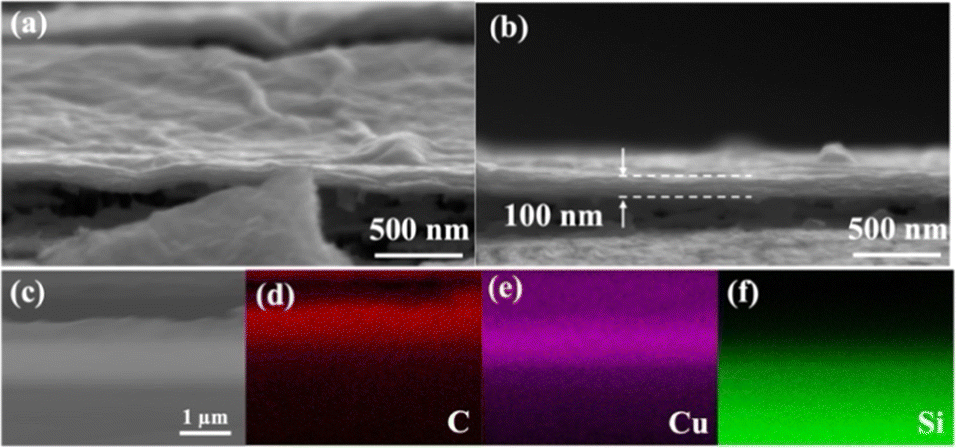 | ||
| Fig. 4 (a) and (b) Cross-sectional SEM image of GO film deposited on MPTS-modified copper at 6 V. (c) EDS mapping image of element (d) C (e) Cu and (f) Si. | ||
In order to improve the conductivity of deposited GO film, electrochemical reduction at room temperature was employed to reduce the GO film. In addition, this reduction method was compared with chemical reduction using NaBH4 reductant and thermal reduction at 200 °C. Fig. 5a shows the Raman spectrum of three specimens reduced in different methods: chemically reduced GO (CRGO), thermally reduced GO (TRGO), and ERGO, respectively. However, reduction temperature is the most important factor affecting the reduction effect of TRGO. At low temperature, only a small amount of oxygen-containing functional groups can be removed. The reduction degree cannot be further improved only by prolonging the reduction time.22 When the GO film was reduced by NaBH4 reducing agent, a large number of bubbles appeared on the surface which destroyed the binding quality of the interface between copper and GO, and even resulted in the fall off of GO film. In addition, the violent reaction breaks the regular structure of the film and introduces additional structural defects. Fig. 5b illustrates the trend of ID/IG at different reduction levels under three reduction methods. As discussed above, the ID/IG value of CRGO is much higher than the pristine GO (0.95) shown by the black dashed line in the graph. TRGO has the lowest ID/IG value because multilayer GO oxidized by the Hummers' method is structurally and chemically metastable. High temperature promotes the spontaneous reduction of GO to graphene.23 But thermal reduction under higher temperature is not studied due to the consideration of practical application scenarios. For ERGO, although electrochemical reduction can reduce the content of oxygen functional groups contained in GO, with the extension of reduction time, the sp2 lattice clusters generated by reduction will lead to the increase of ID/IG value.24 Therefore, the ID/IG value of ERGO decreases first and then increases. According to the variation trend in Fig. 5b, ERGO has the lowest ID/IG value when the reduction time was 1 min.
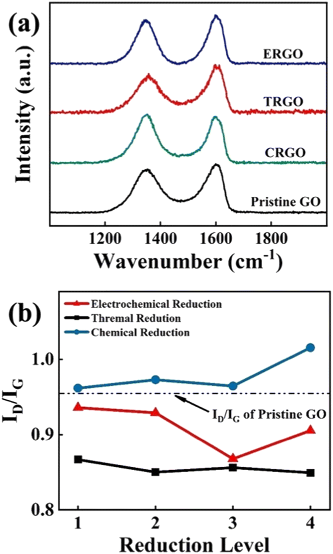 | ||
| Fig. 5 (a) Raman spectrum of GO, TRGO, CRGO, and ERGO. (b) ID/IG of three kinds of RGO, each with four reduction levels (the reduction levels are corresponding to four different specimens in the Experimental section, respectively). The ID/IG of pristine GO is marked as a dotted line in the graph. | ||
ATR-FTIR spectrum of GO and ERGO are shown in Fig. 6a and b. The spectrum shown in Fig. 6a consists of vibratory groups of GO film, including C–O–C (1050 cm−1), Si–O–C (1090 cm−1), CO (1700 cm−1), O–H (∼3200 cm−1),25 and Cu (1250 cm−1).26 After reduction, only few CO and CC (1544 cm−1) were detected and O–H, C–O–C, Si–O–C almost disappeared. The Si–O–C group indicates that some hydroxyl groups on the GO sheets have formed chemical bonds with the hydrolyzed MPTS. The disappearance of oxygen-containing function groups shows that electrochemical reduction method can effectively remove these groups. Furthermore, the peak at ∼3200 cm−1 corresponds to the carboxyl groups (O–H) formed by water molecules.27 The decrease of this peak intensity implies the release of intercalated water which results in a more compacted layer structure than GO.17,28 There are still some remaining groups that haven't been reduced (such as CO) because the reduction of them requires a more negative potential.29 But more negative reduction potential may cause hydrogen evolution on the surface of the working electrode. Hydrogen bubbles can destroy the binding between ERGO and substrate, which is harmful to the quality of ERGO film. Therefore, the scanning voltage of CV analysis is controlled at −0.8–0 V. Fig. 6c and d are the electrochemical test results which exhibit the details during electrochemical reduction process. According to the CV curve, there are two reduction peaks at −0.2 V and −0.75 V, which correspond to the release of intercalated water and the gradual reduction of C–O–C, respectively.29,30 Consistent with the variation trend of CV results, the I–t curve at −0.75 V separated by reduction time indicates that the reduction of C–O is a continuous process because the reduction velocity drops as time extension, especially between the first and the second minute.
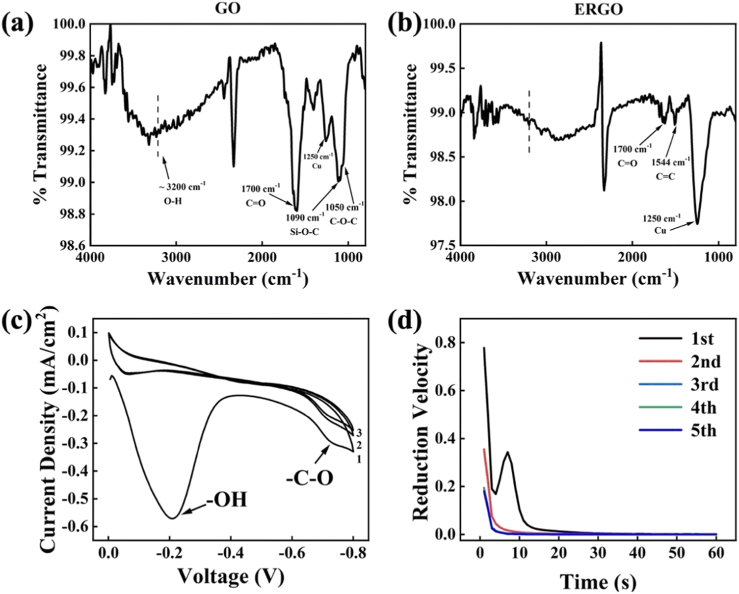 | ||
| Fig. 6 ATR-FTIR of (a) GO and (b) ERGO. The wavenumber is from 800 cm−1 to 4000 cm−1. (c) The first three loops of CV curve scanning from 0 to −0.8 V (vs. reference electrode, 10 mV s−1). (d) I–t curve under −0.75 V (vs. reference electrode) voltage. | ||
The variation of the square resistance of ERGO-Cu, TRGO-Cu and CRGO-Cu with the reduction degree is shown in Fig. 7. The four reduction degrees of all RGO-Cu specimens are corresponding to the experimental conditions in the Experimental section. The square resistance of CRGO-Cu increases significantly with the extension of reduction time because the violent chemical reaction destroys the film quality. As for TRGO-Cu, the removal of oxygen-containing groups is not as good as expected due to the reduction temperature is not high enough. Therefore, it is difficult to achieve a further decrease in square resistance by thermal reduction in this work. The square resistance of ERGO-Cu decreases first and then increase with the extension of the reduction time. The decline of the square resistance corresponds to the removal of some oxygen-containing groups (–OH, C–O–C) and the reduction of structural disorder, while the rise is due to the defects introduced in the electrochemical process. By adjusting the electrochemical reduction time, ERGO-Cu can show optimized square resistance with a 16% decrease compared to the original GO-Cu structure and a 4.5% decrease compared with Cu substrate.
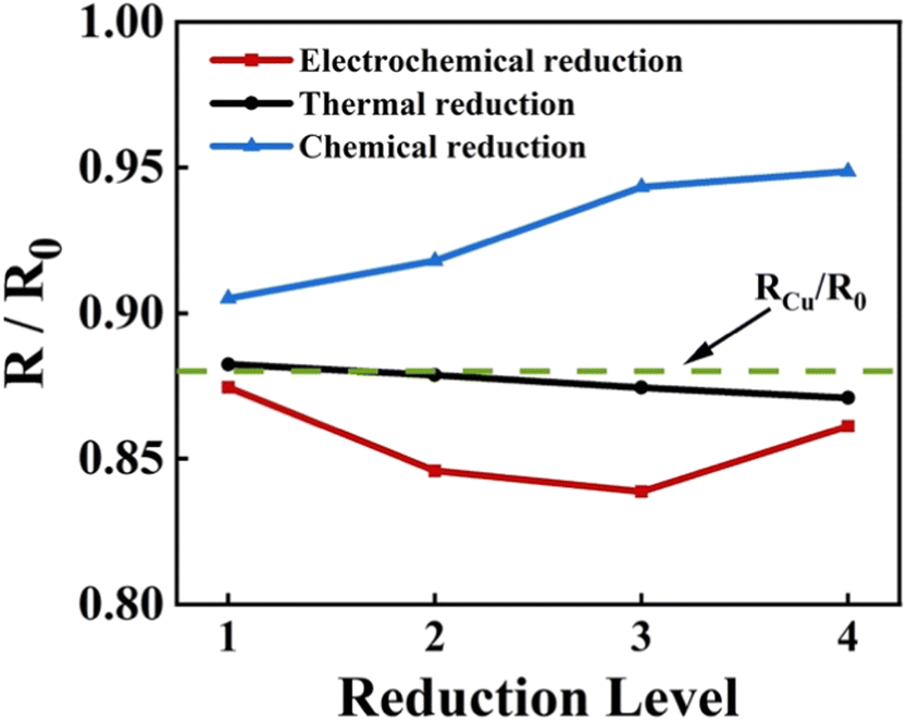 | ||
| Fig. 7 R/R0 of three kinds of RGO under different reduction levels. R0 is the resistance of GO deposited on MPTS-modified Cu without reduction. The square resistance of Cu substrate is marked as a green dash line (RCu/R0 = 0.88). | ||
4 Conclusions
In this work, we realize the room temperature preparation of ERGO-Gu interconnect structure through EPD and electrochemical reduction methods. With the protection of MPTS modification layer, we can obtain a flatter and condense GO-Cu structure in EPD process, with a thickness of nearly 100 nm and a roughness of 13.7 nm. And the chemical bond of GO with hydrolysed MPTS improves the interfacial binding force. Compared with chemical reduction and thermal reduction at 200 °C, electrochemical reduction can realize effective reduction of GO film at room temperature. By adjusting the electrochemical conditions, ERGO-Cu shows a better reduction effect than CRGO-Cu and TRGO-Cu. The optimized ERGO-Cu has 16% lower square resistance than the original GO-Cu structure and 4.5% lower square resistance than the Cu substrate. This research shows the possibility for realizing low-temperature fabrication of graphene-Cu bilayer interconnect structure.Author contributions
Yuan Tian: investigation, data curation, formal analysis, writing – original draft. Silin Han: writing – review & editing. Peixin Chen: investigation. Liang Cao: investigation. Yunwen Wu: supervision, project administration, writing – review & editing. Ming Li: writing – review & editing. Anmin Hu: writing – review & editing.Conflicts of interest
There are no conflicts to declare.Acknowledgements
The work was sponsored by the National Natural Science Foundation of China (No. 62004124).Notes and references
- S. Wang, L. Wang, S. Zhang, H. Zheng, C. Zhang, S. Liu, F. Liu and G. J. Cheng, Vacuum, 2022, 203, 111273 CrossRef CAS.
- C. P. Lee, M. Y. Cai, J. Y. Wang, D. C. Ling, Y. F. Chen, C. S. Wu and J. C. Chen, Phys. Rev. Appl., 2021, 15, 1 Search PubMed.
- J. Deb, N. Seriani and U. Sarkar, Phys. E, 2021, 127, 114507 CrossRef CAS.
- Z. An, J. Li, A. Kikuchi, Z. Wang, Y. Jiang and T. Ono, Microsyst. Nanoeng., 2019, 5, 20 CrossRef PubMed.
- M. Son, J. Jang, Y. Lee, J. Nam, J. Y. Hwang, I. S. Kim, B. H. Lee, M. H. Ham and S. S. Chee, npj 2D Mater. Appl., 2021, 5, 41 CrossRef CAS.
- B. Xu, R. Chen, J. Zhou and J. Liang, Micromachines, 2022, 13, 1–20 Search PubMed.
- C. G. Kang, S. K. Lim, S. Lee, S. K. Lee, C. Cho, Y. G. Lee, H. J. Hwang, Y. Kim, H. J. Choi, S. H. Choe, M. H. Ham and B. H. Lee, Nanotechnology, 2013, 24, 115707 CrossRef PubMed.
- C. H. Yeh, H. Medina, C. C. Lu, K. P. Huang, Z. Liu, K. Suenaga and P. W. Chiu, ACS Nano, 2014, 8(1), 275–282 CrossRef CAS PubMed.
- L. Li, Z. Zhu, T. Wang, J. A. Currivan-Incorvia, A. Yoon and H. S. P. Wong, Tech. Dig. - Int. Electron Devices Meet., 2017, 9, 5.1–9.5.4 Search PubMed.
- I. Deen and I. Zhitomirsky, J. Alloys Compd., 2014, 586, 531–534 CrossRef.
- C. Gan, T. Liang, W. Li, X. Fan, X. Li, D. Li and M. Zhu, Tribol. Int., 2020, 148, 106350 CrossRef CAS.
- G. Jena, S. C. Vanithakumari, S. R. Polaki, R. P. George, J. Philip and G. Amarendra, J. Coat. Technol. Res., 2019, 16, 1317–1335 CrossRef CAS.
- L. Dashairya, D. Das and P. Saha, Mater. Today Commun., 2020, 24, 101189 CrossRef CAS.
- F. Ahmadi and S. Ghasemi, J. Mater. Sci.: Mater. Electron., 2018, 29, 9067–9076 CrossRef CAS.
- A. C. Ferrari, J. C. Meyer, V. Scardaci, C. Casiraghi, M. Lazzeri, F. Mauri, S. Piscanec, D. Jiang, K. S. Novoselov, S. Roth and A. K. Geim, Phys. Rev. Lett., 2006, 97, 1–4 Search PubMed.
- A. C. Ferrari, Solid State Commun., 2007, 143, 47–57 CrossRef CAS.
- D. Li, M. B. Müller, S. Gilje, R. B. Kaner and G. G. Wallace, Nat. Nanotechnol., 2008, 3, 101–105 CrossRef CAS PubMed.
- H. Zhang, S. Wang, Y. Lin, M. Feng and Q. Wu, Appl. Therm. Eng., 2017, 119, 132–139 CrossRef CAS.
- J. Gray-Munro and J. Campbell, Mater. Lett., 2017, 189, 271–274 CrossRef CAS.
- Z. Shang and X. Zhang, Appl. Surf. Sci., 2020, 502, 143853 CrossRef CAS.
- A. Zhou, J. Bai, W. Hong and H. Bai, Carbon, 2022, 191, 301–332 CrossRef CAS.
- J. Cao, G. Q. Qi, K. Ke, Y. Luo, W. Yang, B. H. Xie and M. B. Yang, J. Mater. Sci., 2012, 47, 5097–5105 CrossRef CAS.
- S. Kim, S. Zhou, Y. Hu, M. Acik, Y. J. Chabal, C. Berger, W. De Heer, A. Bongiorno and E. Riedo, Nat. Mater., 2012, 11, 544–549 CrossRef CAS PubMed.
- S. Y. Toh, K. S. Loh, S. K. Kamarudin and W. R. W. Daud, Electrochim. Acta, 2016, 199, 194–203 CrossRef CAS.
- N. J. Huang, Q. Q. Xia, Z. H. Zhang, L. Zhao, G. D. Zhang, J. F. Gao and L. C. Tang, Composites, Part A, 2020, 131, 105797 CrossRef CAS.
- F. Boccuzzi, G. Ghiotti and A. Chiorino, Surf. Sci. Lett., 1987, 183, 285–289 CrossRef.
- M. Yang, J. Zhu, S. Bi, R. Wang and Z. Niu, Adv. Mater., 2022, 34, 1–8 Search PubMed.
- V. C. Tung, M. J. Allen, Y. Yang and R. B. Kaner, Nat. Nanotechnol., 2009, 4, 25–29 CrossRef CAS PubMed.
- M. Gao, Y. Xu, X. Wang, Y. Sang and S. Wang, Electroanalysis, 2016, 28, 1377–1382 CrossRef CAS.
- A. Ambrosi and M. Pumera, Chem.–Eur. J., 2013, 19, 4748–4753 CrossRef CAS PubMed.
Footnote |
| † Electronic supplementary information (ESI) available. See DOI: https://doi.org/10.1039/d2ra07223h |
| This journal is © The Royal Society of Chemistry 2023 |