
 Open Access Article
 This Open Access Article is licensed under a Creative Commons Attribution-Non Commercial 3.0 Unported Licence
Naphthalene diimide-based n-type small molecule organic mixed conductors for accumulation mode organic electrochemical transistors†
Seongdae Kang a,
Jiaxin Fanb,
João B. P. Soaresa and
Manisha Gupta*b
a,
Jiaxin Fanb,
João B. P. Soaresa and
Manisha Gupta*b
aDepartment of Chemical and Materials Engineering, University of Alberta, Edmonton, Alberta T6G 1H9, Canada
bDepartment of Electrical and Computer Engineering, University of Alberta, Edmonton, Alberta T6G 1H9, Canada. E-mail: mgupta1@ualberta.ca
First published on 8th February 2023
Abstract
Organic mixed ionic-electronic conductors (OMIECs), which transport both ionic and electronic charges, development are important for progressing bioelectronic and energy storage devices. The p-type OMIECs are extensively investigated and used in various applications, whereas the n-type ones lag far behind due to their moisture and air instability. Here, we report the synthesis of the novel n-type naphthalene diimide (NDI)-based small-molecule OMIECs for organic electrochemical transistors (OECTs). The electro-active NDI molecule with the linear ethylene glycol side chains is a promising candidate for n-type channel material to obtain accumulation mode OECTs. This NDI-based small-molecule OMIEC, gNDI-Br2, demonstrates ion permeability due to the attachment of the glycol side chains with optimized ionic-electronic conductions. OECT devices with gNDI-Br2 channel material displays excellent performance in water and ambient stability. OECTs fabricated with two different concentrations, 50 mg mL−1 and 100 mg mL−1 of gNDI-Br2 demonstrate a transconductance value of 344 ± 19.7 μS and 814 ± 124.2 μS with the mobility capacitance product (μC*) of 0.13 ± 0.03 F cm−1 V−1 s−1 and 0.23 ± 0.04 F cm−1 V−1 s−1, respectively. These results demonstrate the n-type OMIEC behaviour of the NDI-based small-molecule and its applicability as an OECT channel material.
Introduction
The organic mixed ionic-electronic conductors (OMIECs) have received quite a bit of attention in the past few decades due to their unique conduction mechanism. OMIECs, mostly π-conjugated polymers or small molecule organic conductors, are capable of transporting both the ionic and electronic charges throughout the bulk material.1 The charge transport properties of the mixed conductors can be manipulated by their molecular alignment, ion-penetration capability, material morphology, and crystallinity.2 To date, many OMIECs have been reported and applied to applications including neuromorphic, batteries, and bioelectronics, thanks to their flexibility, low fabrication cost, and biocompatibility.3–5OMIECs have been employed as the active channel material for organic electrochemical transistors (OECTs) because of their redox activity and ability to convert ionic charges to electronic ones.6,7 Unlike the interfacial doping of the organic semiconductors which is involved in the conduction for the organic field-effect transistors, OMIECs can change their doping status by the three-dimensional ion influx from the electrolyte to the channel material.8 The bulk of the electroactive OMIECs channels in the OECTs are doped and dedoped during the measurement by the ionic and electronic mixed conduction with electrolytes.
Poly(3,4-ethylenedioxythiophene) doped with poly(styrene sulfonate) (PEDOT:PSS) is the most common OMIEC material for the OECT active channel.9 It is a hole-transporting p-type material, and PEDOT:PSS-based OECT operates as a depletion mode (normally ON) device.10 PEDOT:PSS based OECT are being used for diverse biosensing applications, including ion, enzyme, and immunosensors.11–13 PEDOT:PSS is a two-component system that blends polyelectrolyte and conjugated polymer based on the OMIECs classification.1,14 Another type of OMIECs material is the block system which is a single molecule conglomerated with ionic and electronic conductors. Block copolymers such as PFO-b-P3PyHY15 and P3EHT-b-PEO16 can be classified as this type of OMIECs. The homogeneous system is another class of OMIECs that has been reported recently. For example, p(g2T-TT)17 and p(gNDI-gT2)18 have the form of the copolymer and provide both ionic and electronic conductions through the whole molecules.
Despite the numerous developments of the p-type OMIECs, the research for an electron transporting n-type one has been far less conducted due to its air and moisture instability and low electron mobility. Only a few studies of n-type OMIECs have been published compared to the p-type materials, including p(gNDI-gT2),18 poly(benzimidazobenzophenanthroline) (BBL),19 NDI-T2 copolymers,20 and 2-(2,3,4-tris(methoxtriglycol)phenyl) [60]fulleropyrrolidine (C60-TEG).21 However, the properties of n-type OMIECs, such as stability in ambient conditions, figure of merit products or charge carrier mobility, are still not comparable to their p-type OMIEC counterparts.22,23 Recently reported NDI-T2 based n-type polymeric material, p(C6-T2), and fused bithiophene imide (BTI) derivatives n-type OMIEC, f-BTI2TEG-FT exhibit figure of merit products of 1.29 and 15.2 F cm−1 V−1 s−1, respectively.24,25
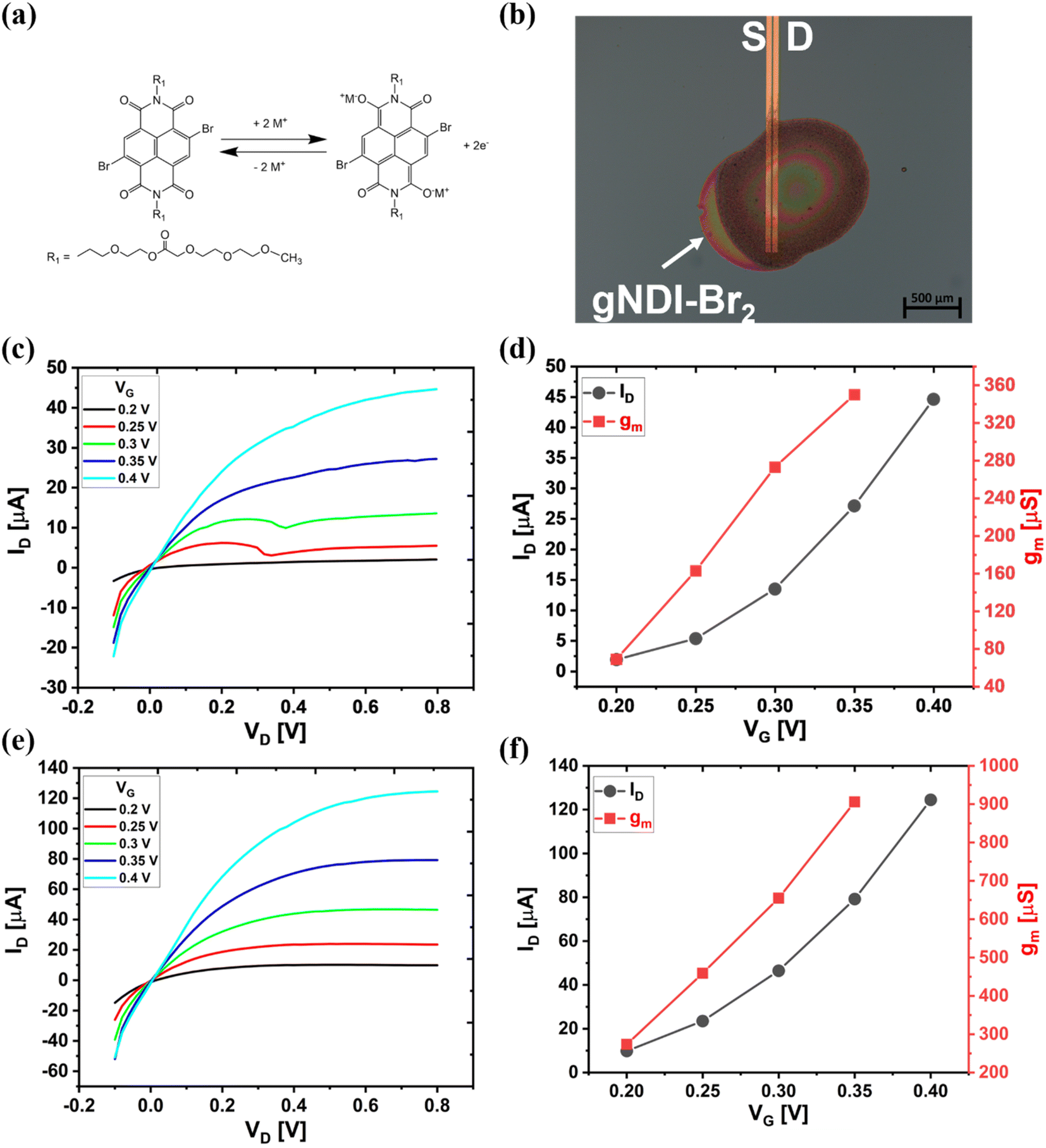
Naphthalenediimide (NDI), one of the rylene diimide derivatives, is a promising n-type organic semiconductor for the applications such as batteries, organic solar cells, and transistors.26–28 Thanks to advantages like material stability and solubility, NDI has been used for numerous organic electronics as a small molecule and applied as an acceptor monomer unit for donor–acceptor (D–A) n-type copolymers.29,30 In 2016, Giovannitti et al. reported the first NDI-based ambipolar D–A copolymer for accumulation mode OECT.18 They synthesized p(gNDI-gT2) copolymer based on NDI acceptor and bithiophene donor with a linear glycolated side chain. The material has a narrow bandgap and is an ambipolar material due to its high electron affinity and low ionization potential value. The polymeric OMIEC is easily processable with an organic solvent such as CHCl3 and has high stability with water and ambient conditions.
In this work, we synthesized a small-molecule NDI-based organic mixed conductor, gNDI-Br2.18 This glycolated NDI small-molecule OMIEC acts as an n-type active channel material for accumulation mode OECTs. NDI small molecule is a typical organic semiconductor that has been used as the channel material for organic field-effect transistors.31 However, the mixed ionic-electronic conduction phenomenon of the NDI-based small-molecule has not been reported for n-type accumulation OECT yet. Here, we demonstrate the potential of the NDI-based small-molecule organic mixed conductor as an active channel material for OECTs with the material's explanation and characterization. Our synthesized gNDI-Br2 thin film exhibited a high volumetric capacitance (C*) of 203.2 F cm−3. We fabricated gNDI-Br2 OECT with two different concentrations, 50 mg mL−1 and 100 mg mL−1, respectively. We observe a transconductance (gm) value of 344 ± 19.7 μS and 814 ± 124.2 μS for 50 mg mL−1 and 100 mg mL−1, respectively. This is the first report of demonstration of NDI small-molecule as an efficient OMIEC. Small molecules are easily solution processed and can be printed and hence this will contribute to the progress of n-type organic semiconductors.
Experimental section
gNDI-Br2 synthesis
2,6-Dibromonaphthalene-1,4,5,8-tetracarboxylic dianhydride was purchased from TCI, and it was used to synthesize gNDI-Br2 with two linear glycol side chains under the N2 atmosphere following the procedure developed by Giovannitti et al.18 The detailed synthesis method is provided in the ESI.†Thin-film preparation
The substrates were cleaned with acetone, isopropanol (IPA), and DI water sequentially for 2 minutes using the sonicator. For each experiment, the gNDI-Br2 was dissolved in anhydrous CHCl3 at different concentrations (5, 10, 20, 30, 40, 50, and 100 mg mL−1). Each concentration of the gNDI-Br2 solution was drop-casted onto a clean substrate, annealed at 40 °C on a hotplate for 24 hours, and kept in the desiccator to ensure the solvent was entirely removed before characterization.Material characterization
1H and 13C were carried out with Varian VNMRS 600. Purified gNDI-Br2 was dissolved in CDCl3, and the spectra were gathered for structural analysis. Attenuated total reflection FT-IR spectrum was collected using Thermo-Nicolet iS50 FT-IR spectrometer. 50 mg mL−1 gNDI-Br2 solution was drop-casted onto the silicon (100) substrate and the transmission was acquired over a spectral range of 4000 to 400 cm−1 with 4 cm−1 resolution and 32 cycles. UV-vis spectroscopy was carried out with PerkinElmer Lambda 900 spectrophotometer to gather the absorbance of the gNDI-Br2 thin film. 50 mg mL−1 gNDI-Br2 solution was drop-casted onto a quartz substrate, and the spectrum was collected over a wavelength range of 300 to 700 nm with a scan speed of 266.75 nm min−1. UPS was performed with Kratos AXIS UPS. The drop-casted thin film of 50 mg mL−1 solution of gNDI-Br2 onto the silicon (100) substrate was used for the experiment. UPS was measured with an HeI source. A −10 V bias was applied to the sample, and the power was 60 W (3 kV × 20 mA).Morphology and crystallinity characterization
Thin films of gNDI-Br2 were prepared by drop-casting the gNDI-Br2 solution with different concentrations (5, 10, 20, 30, 40, 50, and 100 mg mL−1 in CHCl3) onto silicon (100) substrates and imaged using a Zeiss EVO M10 SEM. 50 mg mL−1 gNDI-Br2 solution was drop-casted onto a silicon (100) substrate and annealed at 40 °C for 24 hours. Atomic force microscope was performed in an ambient atmosphere using Bruker Dimension Edge system. Tapping mode was used to image drop-casted gNDI-Br2 thin film (50 mg mL−1) on a silicon (100) substrate. Sample roughness was calculated by Nanoscope Analysis software. GIWAXS was carried out at the Canadian Light Source at Brockhouse diffraction sector-undulator beamline (BXDS-IVU). 50 mg mL−1 gNDI-Br2 solution was drop-casted to form a thin film on a silicon (100) substrate for the experiment. The applied energy was 9.96 keV with an incidence angle of 0.2°, and the sample to the Rayonix MX300HE 2D detector distance was 588.7 mm with the LaB6 standard calibration. The 2D data was analyzed with GSAS II and GIXSGUI software.32 GIXRD was performed by the Bruker D8 discover with a Vantec-500 2D detector. The data was collected from the incidence angle of 2θ from 1.2° to 30° with a step size of 0.01°.Electrochemical characterization
Gamry Reference 600+ potentiostat with the standard three-electrode configuration was used for all electrochemical characterizations. For the Spectroelectrochemical measurement, gNDI-Br2 thin film deposited onto ITO coated glass slide was used as the working electrode. This film was immersed in 100 mM NaCl with a platinum counter electrode and an Ag/AgCl (in 3 M NaCl) reference electrode in a 3 mL standard cuvette. A negative bias of −0.6 V to 0 V with a step size of 0.1 V was applied to the gNDI-Br2 film with respect to the Ag/AgCl. The absorbance spectrum was measured with PerkinElmer Lambda 900 spectrophotometer at each applied potential. The scan range is from 300 to 700 nm with a scan speed of 266.75 nm min−1. Before the electrochemical cyclic voltammetry of gNDI-Br2, Ag/AgCl reference electrode was calibrated using 5 mM of K4Fe(CN)6 in acetonitrile with 100 mM tetrabutylammonium hexafluorophosphate (TBAPF6) supporting electrolyte. Then, 5 mM of gNDI-Br2 was dissolved in freshly-degassed acetonitrile with 100 mM of TBAPF6 supporting electrolyte. For three-electrode system, two of platinum wires were used for counter and working electrodes and a Ag/AgCl in 3 M KCl was used as the reference electrode. The potential was applied from −0.8 to 1.3 V with a scan rate of 50 mV s−1 and a step size of 1 mV. Cyclic voltammetry was measured for five cycles, and the second cycle was used for the analysis. The working electrode was prepared for the electrochemical impedance spectroscopy by drop-casting gNDI-Br2 thin-film from the 50 mg mL−1 solution on top of the aerosol jet printed gold electrode on a 125 μm polyimide substrate. An experiment was performed using a platinum counter and Ag/AgCl (in 3 M NaCl) reference electrode in 100 mM NaCl electrolyte. The frequency range of 100 kHz to 0.1 Hz for an AC voltage of 10 mV rms was used. During the measurement, specific DC potential applied from +0.1 to −0.3 V with a step size of 0.1 V. The capacitance was estimated using the Randles equivalent circuit, R(R||C). All electrochemical measurement data were analyzed using the Gamry Echem Analyst software.OECT device fabrication and characterization
For the source/drain electrode fabrication, Si/SiO2 substrates were thoroughly cleaned using piranha solution, and hexamethyldisilazane (HMDS) was deposited in the oven for 15 min. AZ 5214E photoresist was spin-coated and baked, and exposed with a photomask using a mask aligner and developed with an MF-319 developer for patterning the electrodes. 5 nm of titanium (Ti) and 100 nm of gold (Au) was deposited via the magnetron sputtering system, and lift-off was performed with acetone to obtain the source and drain electrodes. 0.2 μL of 50 mg mL−1 and 100 mg mL−1 gNDI-Br2 solution was drop-casted between the source and drain electrodes to form an active channel for OECT. A 100 mM NaCl solution was applied onto the gNDI-Br2 OECT channel, and an Ag/AgCl gate electrode was placed in the electrolyte without touching the channel surface. The electrical measurement was conducted using Keithley 2612b sourcemeter controlled by a customized LabVIEW. Current–voltage (IV) characteristics were collected with the gate voltage (VG) was stepped from 0.2 V to 0.4 V with an increment of 0.05 V while sweeping the drain voltage (VD) from −0.1 V to 0.8 V with an increment of 0.02 V. The OECT device was tested 8–10 times to confirm its repeatability. The device was rinsed with DI water to remove NaCl electrolyte residue between the different measurements. The repeated cycling measurement was carried out with a BK precision 4055 function waveform generator and a Keithley 2612b sourcemeter controlled by a custom-made LabVIEW. While applying a constant bias at the drain, a rectangular wave gate voltage with an amplitude of 0.5 V, the pulse width of the 30 s, and a 50% duty cycle was applied at the gate for 36 min, and the drain current was measured.Results and discussion
Synthesis of gNDI-Br2
gNDI-Br2 synthesis scheme is depicted in Fig. S1 in the ESI.† Originally, gNDI-Br2 was used as a monomer for the first reported n-type OMIEC for OECT, p(gNDI-gT2).18 We synthesized gNDI-Br2 monomer and tested its possibility for OMIEC material. NMR was executed to analyze the structure, and 1H and 13C-NMR spectra are provided in Fig. S2 and S3.† FT-IR was conducted to confirm the material structure from the NMR result, and the spectrum is in Fig. S4.† Fig. S5† is the ESI-TOF mass spectrum and it was performed with Agilent TOF 6220. The calculated mass by the ESI-ToF is 918.11 g mol−1, and it corresponds to the molecular mass of gNDI-Br2.18Material morphology
To investigate the material morphology and crystallinity of the gNDI-Br2 thin-film, SEM, GIWAXS, and GIXRD were performed. Fig. 1 and ESI Fig. S6† show the SEM images of thin films made from drop-casting gNDI-Br2 with different concentrations (5–100 mg mL−1). The film continuity is one of the important features for OMIECs to connect and provide conductivity to the source/drain electrodes. A continuous gNDI-Br2 thin film acts as an active channel in the OECT, and SEM has been employed to find out gNDI-Br2 thin film morphology.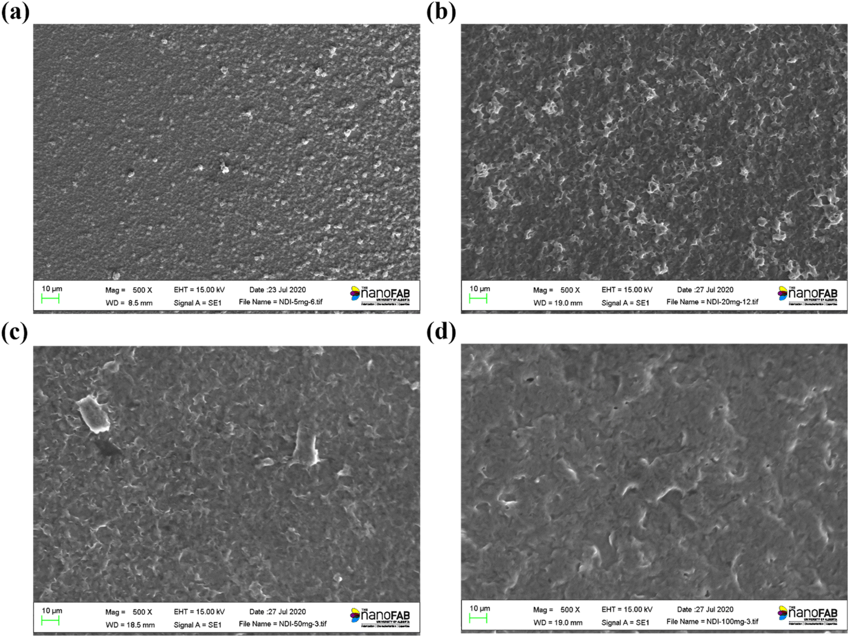 | ||
| Fig. 1 Scanning electron microscopy (SEM) images of gNDI-Br2 thin films with different concentrations. (a) 5 mg mL−1, (b) 20 mg mL−1, (c) 50 mg mL−1, (d) 100 mg mL−1. | ||
Fig. 1(a) (5 mg mL−1) shows that the material does not fully spread onto the substrate due to the low weight percentage of gNDI-Br2 solution and the film has lots of voids. Due to the high volatility of the CHCl3, gNDI-Br2 thin-film possesses voids leading to a discontinuous film with thickness variation. With the increment of the gNDI-Br2 concentrations, material morphology is improved. Fig. 1(b) and S6(a)–(c)† are the samples for the 10, 20, 30, and 40 mg mL−1 of gNDI-Br2. This film still has voids and agglomerated gNDI-Br2 molecules, but the amount of unoccupied parts between the self-assembled NDI molecules decreases as the solution concentration increases.
Fig. 1(c) and (d) show the SEM images for the thin films deposited using 50 and 100 mg mL−1 gNDI-Br2, respectively. With a solution concentration higher than 50 mg mL−1 gNDI-Br2 we observe a continuous thin film as seen in the enlarged view (1000× in 50 mg mL−1) shown in Fig. S6(d).† Densely packed thin films of NDI cause the improvement of the electronic conductivity of the gNDI-Br2 organic mixed conductor. The molecular entanglement facilitates π–π interaction and leads to higher intermolecular charge transfer, contributing to the improved charge transport of this gNDI-Br2 thin films. To measure the gNDI-Br2 thin film roughness, atomic force microscopy was used. Fig. S7† shows the AFM scan of a 50 mg mL−1 gNDI-Br2 solution drop-casted film with root-mean-square roughness (Rq) of 375 nm.
The drop-casted gNDI-Br2 thin film microstructure was observed by the two-dimensional grazing incidence wide-angle X-ray scattering (GIWAXS) to elucidate material morphology. The NDI small-molecule organic semiconductors are well-known as brick-wall packing materials deposited by sublimation or vapour technique. Due to the enhanced π–π interaction between the polycyclic naphthalene ring in the NDI core molecules (Fig. 2(a)), piled-up NDI organic semiconductors retain high electronic charge mobility.33 However, as Fig. 2(b) depicts, solution-processed gNDI-Br2 demonstrates ring-like shapes, unlike other OMIECs or NDI derivatives. The isotropic 2D GIWAXS patterns demonstrate that the gNDI-Br2 molecules are irregularly stacked on the substrate, and there is no favoured crystallographic arrangement.34,35
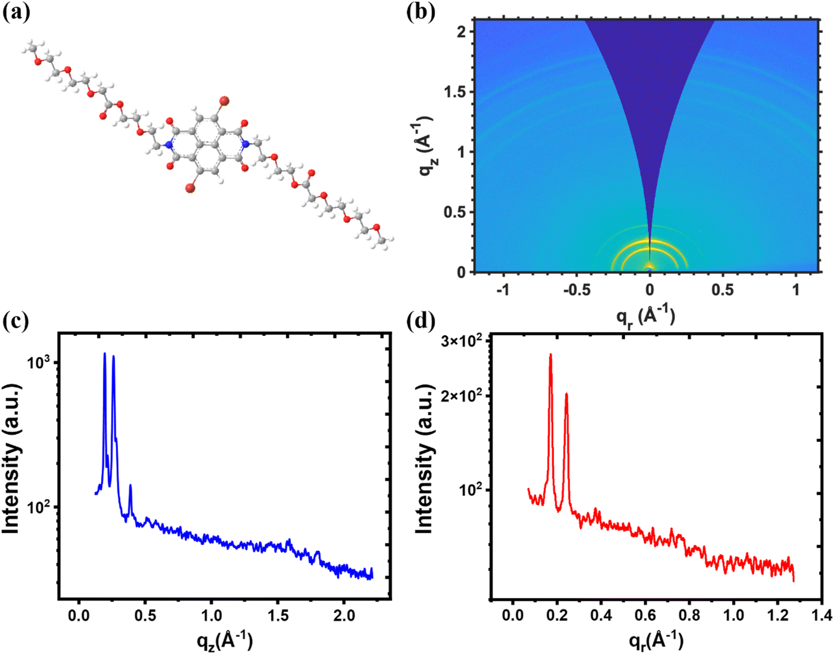 | ||
| Fig. 2 (a) Illustration of gNDI-Br2 crystal structure (b) GIWAXS patterns of the gNDI-Br2 thin film. (c) Line cuts of out-of-plane qz direction, and (d) in-plane qr of gNDI-Br2. | ||
The gNDI-Br2 molecular skeleton is illustrated in Fig. 2(a), and the distance between any two atoms is calculated using ChemBio3D software. There are two possible packing motifs of lamellar stacking for the NDI small-molecules, herringbone and brick-wall stacking.36,37 The 2D GIWAXS patterns in Fig. 2(b) show ring-like scattering, and it provides peaks at similar q vectors. In the out-of-plane and in-plane line cuts, two significant and sharp reflections are observed, and it represent herringbone and brick-layer stacking motifs.
The calculated d-spacing from the first strong peak appears at qz = 0.195 Å−1 (d = 32.22 Å) in Fig. 2(c) and qr = 0.185 Å−1 (d = 33.96 Å) in Fig. 2(d). It is shorter than the estimated gNDI-Br2 molecules, including the linear glycol side chains (∼42.57 Å). This indicates a herringbone motif of lamellar-like scattering of the gNDI-Br2 with a maximum angle of ∼23° on both qr and qz direction. Another possible lamellar-like scattering of gNDI-Br2 is a brick-layer motif. The intermolecular d-spacing between each gNDI-Br2 molecule is ∼23 Å. The observed peaks observed at qz = 0.262 Å−1 (d = 23.98 Å) and qr = 0.255 Å−1 (d = 24.64 Å) from in-plane and out-of-plane line cuts match this brick-layer motif intermolecular d-spacing well.
The fully extended length of the linear glycolated side chain of the gNDI-Br2 is 18.78 Å. Due to this, the third strongest out-of-plane peak measured at qz = 0.389 Å−1 (d = 16.2 Å) in Fig. 2(c) implies edge-to-face stacking interaction between two gNDI-Br2 molecules.38 There are weak out-of-plane scattering peaks at higher qz = 1.59 Å−1 (d = 3.95 Å), and 1.8 Å−1 (d = 3.49 Å). Weak and small peaks represent the π–π spacing between the core of the NDI molecules. These peaks are observed only in out-of-plane line cuts and they indicate two different spacing due to the irregular distribution and entanglement of the gNDI-Br2 molecules.
GIXRD result of gNDI-Br2 was measured to confirm the result of GIWAXS. In Fig. S8(b),† it only shows the out-of-plane line cuts along with qz direction, unlike GIWAXS. For the qz direction peaks, due to the higher incidence angle of the GIXRD (1.2°) than GIWAXS (0.2°), GIXRD cannot detect the peak at qz = 0.159 Å−1. The measured peak at GIXRD at qz = 0.261 Å−1 corresponds to the GIWAXS peak at qz = 0.262 Å−1. Other significant peaks from GIXRD are qz = 1.31, 1.46, and 1.61 Å−1. These are similar to the GIWAXS weak and broad peak at qz = 1.59 Å−1.
Material optical and electrochemical properties
The reduction–oxidation ability and HOMO/LUMO level of gNDI-Br2 were investigated by electrochemical cyclic voltammetry in organic solution, and the result is depicted in Fig. 3(a). The reduction reaction of gNDI-Br2 between neutral and reduced states was observed from 0 to −0.5 V. Tetrabutylammonium cations in the electrolyte compensate for the negatively charged gNDI-Br2 molecules during the reduction. The LUMO level of the gNDI-Br2 was calculated from the reduction onset (Ered) on cyclic voltammogram, and it was 4.12 eV. This high LUMO level contributes to the air and moisture stability of the NDI material, which makes this gNDI-Br2 small molecule very stable and suitable as OECT channel material.39 In addition, gNDI-Br2 demonstrated the oxidation reaction between 0.9 and 1.2 V and the calculated HOMO level from oxidation onset (Eox) is 5.33 eV.40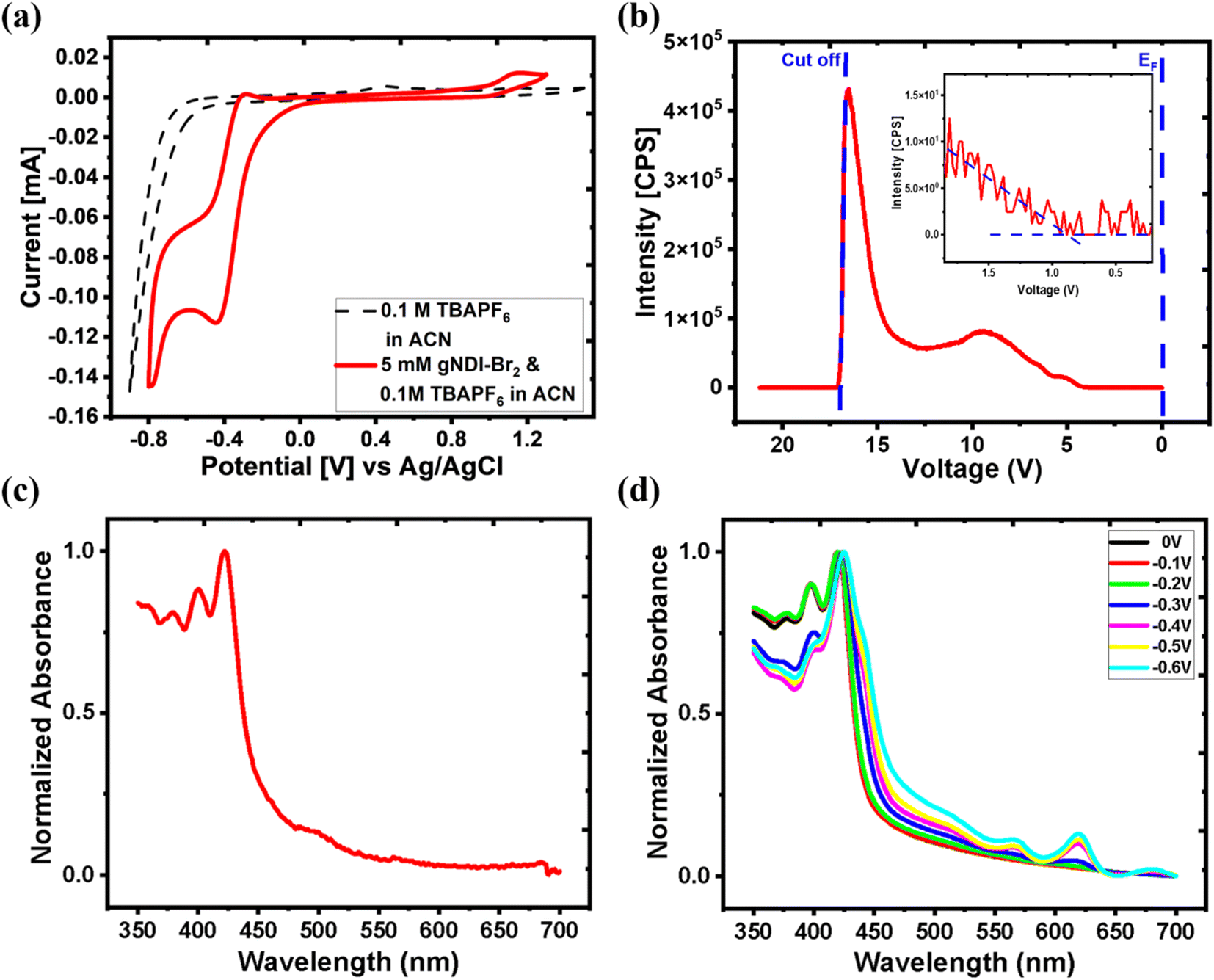 | ||
| Fig. 3 (a) Solution cyclic voltammetry of gNDI-Br2 in acetonitrile. (b) Ultra-violet photoelectron spectroscopy of gNDI-Br2 thin film. (c) UV-vis spectrum of the thin-film gNDI-Br2. (d) Spectroelectrochemical measurement of the gNDI-Br2. | ||
Ultraviolet photoelectron spectroscopy (UPS) was performed to determine the ionization potential (IP) of gNDI-Br2 in vacuo, and the spectrum is depicted in Fig. 3(b). The IP of the gNDI-Br2 small-molecule organic semiconductor can be calculated to be 5.2 eV using eqn (1).41
| Ionization potential (IP) = hν − Ecut-off + EHOMO | (1) |
UV-vis absorption spectrum of the gNDI-Br2 on the solid-state is depicted in Fig. 3(c). From the UV-vis absorption spectrum, three absorption peaks (λmax) were observed at 380 (λ1), 401 (λ2), and 422 (λ3) nm. The intensity of absorption maxima decreases as the wavelength increases (λ3–λ2–λ1). All three λmax are the result of the π–π* transition between the NDI molecules.42 Unlike the D-A polymer, p(gNDI-gT2), gNDI-Br2 only shows π–π* transition, not the broad intramolecular charge transfer (ICT). The optical bandgap (Eg,opt) is 1.83 eV, extracted using the Tauc plot method.
Spectroelectrochemical measurement was carried out to study the electrochemical doping process of gNDI-Br2. The electrochemical interaction between ion and gNDI-Br2 can be observed by applying a specific potential range to the material. This change in doping modulates material electrochromic properties and affects the absorption spectra.43 Fig. 3(d) is the spectroelectrochemical measurement result of gNDI-Br2, and it shows two new absorption peaks at 565 and 620 nm after applying a DC potential of −0.4 V. This change of absorption spectra from the spectroelectrochemical measurement at −0.4 V correlates with the reduction peak from the cyclic voltammetry of gNDI-Br2. The gNDI-Br2 is reduced from the neutral state when a higher negative potential is applied, and the intensity for both absorption peaks increases. In the −0.3 to −0.6 V range the π–π* absorption peaks at 380 nm (λ1) and 401 nm (λ2) for diminish but the peak at 420 nm (λ3) is still present. Once the applied voltage is higher than −0.6 V, a significant decrease of absorbance was observed due to over-reduction and delamination of the gNDI-Br2 film. As the absorption properties vary with the change of the electronic band structures, the spectroelectrochemical measurement confirms that gNDI-Br2 has the bulk doping transition capability, which is essential for being applicable as the OECT channel material.44
Table 1 summarizes the optical and electrochemical measurement data for the synthesized gNDI-Br2. gNDI-Br2 optical bandgap (Eg,opt) was extracted from the thin-film UV-vis spectroscopy as 1.83 eV. The IP of this material was measured by UPS and corroborated by the CV measurement. The IP from the UPS and HOMO level from cyclic voltammetry are 5.2 eV and 5.33 eV, respectively, which indicates that both techniques give us similar results. The electrochemical bandgap ΔE was estimated as 1.21 eV using the HOMO and LUMO level from the CV. This narrow bandgap of gNDI-Br2 facilitates charge injection by reducing the barrier between the gold source/drain electrodes to the material.45
| Material | Eg,opta [eV] | IPb [eV] | Eoxc [V] | Eredc [V] | EHOMOd,g [eV] | ELUMOe,g [eV] | Bandgapf [eV] |
|---|---|---|---|---|---|---|---|
| a Calculated from the Eonset of UV-vis spectrum.b Ionization potential (IP) measured by UPS.c Measured from electrochemical cyclic voltammogram.d HOMO level (EHOMO) was calculated by the equation, EHOMO = e[Eox − E1/2(ferrocene) + 4.8] V.40e LUMO level (ELUMO) was calculated by the equation, ELUMO = e[Ered − E1/2(ferrocene) + 4.8] V.40f Band gap was calculated from EHOMO and ELUMO from cyclic voltammetry (ΔE = EHOMO − ELUMO).g Cyclic voltammetry of ferrocene was measured, and E1/2(ferrocene) was calculated from the ferrocene cyclic voltammogram in Fig. S9. | |||||||
| gNDI-Br2 | 1.83 | 5.2 | 0.97 | −0.24 | 5.33 | 4.12 | 1.21 |
The effective capacitance values of OMIECs determine the feasibility of the material as the active channel for OECTs. OECTs require volumetric doping through the entire OMIECs material, whereas the electrolyte-gated organic field-effect transistor (EGOFET) channel only requires a field-effect capacitive process at the interfaces between the channel material and electrolytes.46 Effective capacitance values of the OMIECs for OECTs are more significant than the ones for EGOFETs,47 and this can be extracted from the electrochemical impedance spectroscopy (EIS). gNDI-Br2 coated gold working electrode (3.23 × 10⁻³ cm2) was immersed into the electrochemical cells with 100 mM NaCl electrolyte solutions to conduct the EIS measurements, shown in Fig. 4. The effective capacitance per unit area at the applied DC potential of −0.3 V is estimated as 2.46 × 10⁻² F cm−2. The thickness of the gNDI-Br2 thin film measured by a profilometry is 1.21 μm, and the volumetric capacitance (C*) was extracted to be 203.2 F cm−3. This value is comparable to the C* value of C60-TEG (220 ± 50 F cm−3), previously reported n-type small-molecule OMIEC.21
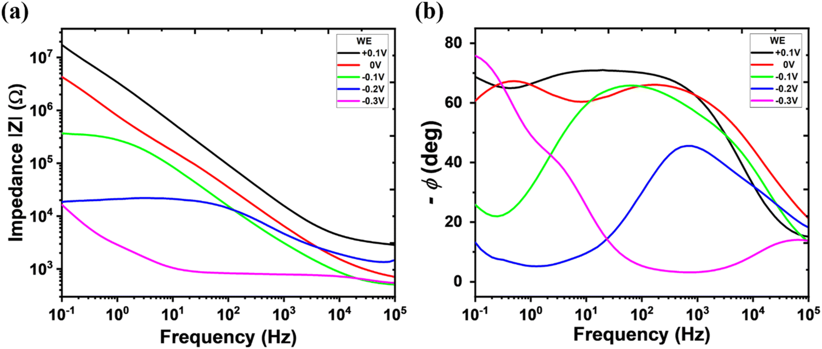 | ||
| Fig. 4 (a) Impedance and (b) phase angle Bode plot of gNDI-Br2 from the electrochemical impedance spectroscopy. | ||
The high volumetric capacitance of gNDI-Br2 with the comparison of the EGOFET channel material tells another possibility of material as an OMIEC, not only the organic semiconductors. Owing to its high effective capacitance, the synthesized gNDI-Br2 can accumulate charges throughout the entire volume of the channel. The reduction–oxidation behaviour from the CV, bulk doping capability from the spectroelectrochemical results, and high volumetric capacitance value from the EIS are significant evidence that this gNDI-Br2 can be a strong candidate for the new type of OMIECs material.
As a small molecule organic mixed conductor, the NDI molecule has strong π–π intermolecular interactions between the NDI core naphthalene rings. The two-electron reaction is expected from the NDI from the polycyclic rings of the naphthalene molecule. It makes the NDI a redox-active material due to the transport of the electron between the NDI molecule and electrolyte.48 Fig. 5(a) represents a feasible electrochemical reduction reaction of gNDI-Br2 with metal ions such as Na+ or K+ from the electrolyte. Two carboxylic oxygen at the NDI naphthalene rings can be coupled with the metal ions as an active site. The excess electron from the reduction process of the NDI can transport to the other NDI molecules through its π-conjugated structure. This reduction reaction of NDI small molecules with electrolytes gives the prospect of an n-type active channel material for OECTs. The electrochemical response of the gNDI-Br2 is described in eqn (2).
| gNDI-Br2 + 2M+ + 2e− ↔ gNDI-Br2− + 2M+ | (2) |
 | ||
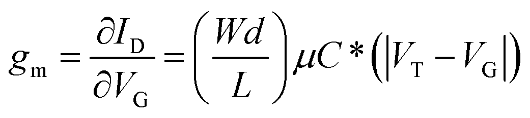
| Fig. 5 (a) The chemical structure of gNDI-Br2 and its electrochemical reduction reaction scheme with metal ions. (b) Microscopic image of a 50 mg mL−1 gNDI-Br2-based OECT with channel width (W) of 1081 μm, length (L) of 10 μm, and thickness (d) of 1.3 μm. (c), (d) Output characteristics of the n-type gNDI-Br2 (50 mg mL−1) OECT measured with 100 mM NaCl electrolyte and Ag/AgCl gate electrode and transfer and transconductance curve at VD = 0.8 V. (e), (f) Output characteristics of the n-type gNDI-Br2 (100 mg mL−1) OECT measured with 100 mM NaCl electrolyte and Ag/AgCl gate electrode and transfer and transconductance curve at VD = 0.8 V. | ||
The linear ethylene glycol side chain attached to the NDI core molecule provides better solubility and ionic conductivity. Without additional side chains, NDI can only be dissolved in few halogenated and aromatic solvents which are complicated to remove.28 By adding the glycol side chains to the NDI, gNDI-Br2 can be dissolved in common organic solvents, such as acetone and CHCl3. The improved solubility of gNDI-Br2 facilitates device fabrication with low temperature solution-based techniques such as drop-casting and spin-coating. In addition, the hydrophilic glycol chains at both sides of the gNDI-Br2 will attract water molecules and ions. Injected ions can be transported along the glycol side chains of a gNDI-Br2 molecule and in between neighboring gNDI-Br2 molecules, which assists in the ionic conduction and electrochemical doping of the material.1
The microscopic image of the small-molecule OECT was depicted in Fig. 5(b), and the IV characteristics were obtained with 100 mM NaCl electrolyte and Ag/AgCl gate electrode. The output characteristics of the 50 mg mL−1 gNDI-Br2 OECT device is shown in Fig. 5(c), it can be seen that the drain current (ID) increases with the drain potential (VD) under constant gate voltage (VG); clearly demonstrating that this gNDI-Br2 is an n-type channel material. The device is normally OFF at VG = 0 and turns ON when a VG higher than the threshold voltage (VT) is applied. As seen from the transfer curve, ID increases as the VG increases; therefore, this gNDI-Br2-based OECT works as an accumulation mode device. Increased VG causes the reduction of the gNDI-Br2 active channel, and the metal ions from the electrolyte migrate from the electrolyte to compensate material's electron balance.46
Fig. 5(d) shows the transfer curve and the corresponding transconductance (gm) curve for the 50 mg mL−1 gNDI-Br2 OECT. For the OECT we obtain a maximum drain current (ID,max) of 44.6 μA with a transconductance (gm) of 344 ± 19.7 μS, and the ON/OFF (ION/OFF) ratio of ∼101. Normalized transconductance (gm,norm) calculated from the gm and channel dimensions is 0.024 ± 0.003 S cm−1. The material figure of merit, μC* product, was calculated using eqn (3) with the device geometry and the VT of 172.5 mV (Fig. S10†).22
 | (3) |
At the maximum gm, μC* was calculated as 0.13 ± 0.03 F cm−1 V−1 s−1. This value is not as high as the μC* of C60-TEG (∼7.0 F cm−1 V−1 s−1),21 but similar to the other NDI-based polymeric OMIECs channel materials, p(C3-gNDI-gT2) (0.13 F cm−1 V−1 s−1)49 and p(C8-T2) (0.13 ± 0.074 F cm−1 V−1 s−1).24 With this μC* figure of merit and the capacitance value from the EIS result, the electron mobility of gNDI-Br2 can be extracted. The calculated μ value from eqn (3) is 6.4 × 10⁻⁴ ± 1.3 × 10⁻⁴ cm2 V−1 s−1. This mobility value is similar to the electron mobility of BBL, which is 7.0 × 10⁻⁴ cm2 V−1 s−1.19
Two different W/L devices were fabricated with channel length of 10 and 20 μm using the synthesized gNDI-Br2. Fig. 5(c) and (d) and S11† show the output characteristics, transfer and transconductance curve for these devices. The average transconductance (gm) values are 344 ± 19.7 and 149.1 ± 25.4 μS for each L = 10 and L = 20 μm device. Both the devices have the same channel thickness (d) and μC*. The device current and the transconductance obtained from these devices are in accordance of their W/L ratios of 108.1 and 43.5 for L = 10 and L = 20 μm, respectively.50,51 Fig. 5(e) and (f) show 100 mg mL−1 gNDI-Br2 OECT IV characteristics. This device fabricated with higher concentrations of gNDI-Br2 solution and the W/L ratio is 130.1 with length (L) of 10 μm. Compared to the 50 mg mL−1 device, the increased concentrations of gNDI-Br2 shows maximum transconductance (gm) of 814 ± 124.2 μS and mobility capacitance product (μC*) of 0.23 ± 0.04 F cm−1 V−1 s−1, respectively. The additional amount of gNDI-Br2 molecules enhances device transconductance and mobility capacitance product by creating a denser thin film. As the material conducts via hopping, denser films lead to higher transconductance.
For biosensing applications, the device needs to operate stably in aqueous environment. The gNDI-Br2 OECTs consistently demonstrated similar output and transfer characteristics over 5 measurements (ID,max 54.1 ± 8.5 μA at VD = 0.8 V and VG = 0.4 V with 50 mg mL−1 gNDI-Br2). In addition, the repeated cycling measurements of this OECT device (Fig. S12†) were performed gate potential between 0 and 0.5 V in the constant bias (VD = 0.5 V, pulse length = 30 s) over 36 minutes. We observe 22.3% drain current reduction after 36 minutes. But it can be observed that the reduction after 800 s the reduction in the drain current is only 5.65% till the end of measurement. We think that some of the cations are trapped in the material permanently after the initial testing and this leads to a reduction in the device current. Single-pulse from the repeated cycling measurements is shown in Fig. S12(c).† The NDI active channel requires a longer ON pulse time to reach the saturated ID regime as compared to the other n-type OMIEC material. Due to the larger thickness of the gNDI-Br2 film, the ionic charges, such as metal ions, take extra time to penetrate through the film. Hence, it requires more time to dope the material volumetrically.
Table 2 summarizes the relevant results from literature related to NDI-based polymeric and small molecule OMIECs and the fabricated OECT performance. A few research studies have been published for the n-type OMIECs, but this is the first reported NDI-based small molecule channel material for OECT. Compared to other n-type OMIECs, gNDI-Br2 with glycol side chains shows similar μC* value than p(C8-T2)24 and p(C3-gNDI-gT2),49 which was based on gNDI-Br2 monomer. The synthesis procedure we have used is relatively more straightforward and less toxic as compared to the other polymeric OMIECs because it operates without a transition-metal catalyst. However, the gNDI-Br2 shows a lower gm,norm than other NDI-based polymeric materials, even with a lessened figure of merit products. Feng et al.25 have published new fused bithiophene imide-based n-type OMIECs, f-BTI2TEG-T and f-BTI2TEG-FT. Between the two fused BTI OMIECs, f-BTI2TEG-FT demonstrates the highest normalized transconductance (gm,norm) and mobility capacitance product (μC*) values, 4.6 S cm−1 and 15.2 F cm−1 V−1 s−1 for f-BTI2TEG-FT, among the other reported n-type OECT channel materials. This material shows enhanced transconductance and μC* due to the strong water uptake and ion transport. To obtain better OECT performance and stability with this n-type small molecule OMIEC, different device configurations or the channel fabrication method will be tried in the future. In addition to this, different glycol side-chain structures or other core structures such as thiophene fused NDI can be adapted to improve the peak performance of NDI small molecules. With the demonstrated n-type small molecule, the accumulation mode complementary OECT device for inverters can be fabricated.11 These devices can be utilised for both sensing and signal processing applications for flexible electronics and biosensors.
| W/L | Conc. | gm (μS) | gm,norma (S cm−1) | C*b (F cm−3) | μec (cm2 V−1 s−1) | μC*d (F cm−1 V−1 s−1) | ION/OFF | Ref. | |
|---|---|---|---|---|---|---|---|---|---|
| a gm,norm value calculated by the channel geometry (Wd/L).b The capacitance C* value calculated from EIS result.c The maximum μe value extracted from the figure of merit (μC*) and volumetric capacitance (C*).d The maximum μC* value extracted using equation gm = (Wd/L)(μC*) × (Vth − VG).e The μ value of p(gNDI-gT2), p(C3-gNDI-T2), and p(C6-gNDI-T2) extracted from their OFET measurement. | |||||||||
| gNDI-Br2 | 108.1 | 50 mg mL−1 | 344 ± 19.7 | 0.024 ± 0.001 | 203.2 | 6.4 × 10⁻⁴ ± 1.3 × 10⁻⁴ | 0.13 ± 0.03 | 15 ± 7.5 | This work |
| 43.5 | 149 ± 25.4 | 0.02 ± 0.003 | 7.0 × 10⁻⁴ ± 4.8 × 10⁻⁵ | 0.14 ± 0.01 | 9.7 ± 6.1 | ||||
| 130.1 | 100 mg mL−1 | 814 ± 124.4 | 0.037 ± 0.006 | — | — | 0.23 ± 0.04 | 13.4 ± 3.4 | ||
| p(gNDI-gT2) | 10 | 5 mg mL−1 | 21.7 | — | 397 | 1.0 × 10⁻⁵e | 0.18 | 3.2 × 10³ | 18 |
| BBL | 1950 | 2 mg mL−1 | 9700 | — | 930 ± 40 | 7.0 × 10⁻⁴ | — | 6 × 10³ | 19 |
| NDI-T2 (P90) | 10 | 5 mg mL−1 | 47 | 0.21 | 198.2 | 2.38 × 10⁻⁴ | — | — | 20 |
| C60-TEG | 20 | 10 mg mL−1 | 4.1 ± 0.5 | — | 220 ± 50 | 3 × 10⁻² | 7.0 ± 2.0 | — | 21 |
| p(C2-T2) | 10 | 15 mg mL−1 | — | 0.4 | 492 | 3.97 × 10⁻⁴ ± 3.05 × 10⁻⁵ | 0.2 ± 0.015 | 104 | 24 |
| p(C4-T2) | 10 | — | 0.63 | 158 | 1.9 × 10⁻³ ± 1.88 × 10⁻⁶ | 0.3 ± 0.0003 | 105 | 24 | |
| p(C6-T2) | 10 | — | 2.28 | 272 | 4.74 × 10⁻³ ± 4.31 × 10⁻⁴ | 1.29 ± 0.117 | 104 | 24 | |
| p(C8-T2) | 10 | — | 0.15 | 342 | 3.76 × 10⁻⁴ ± 2.17 × 10⁻⁴ | 0.13 ± 0.074 | 105 | 24 | |
| p(C3-gNDI-gT2) | 10 | 4 mg mL−1 | — | 0.34 | 72 | 9.2 × 10⁻⁴e | 0.13 | — | 50 |
| p(C6-gNDI-gT2) | 10 | — | 0.37 | 59 | 6.3 × 10⁻⁴e | 0.16 | — | 50 | |
Conclusions
Here, we report the development of novel n-type naphthalene diimide (NDI)-based small-molecule organic mixed ionic and electronic conduction for application in organic electrochemical transistors (OECTs). We have investigated the promising features of gNDI-Br2 small molecule mixed conductor as the channel material for n-type accumulation mode OECTs. The synthesized material demonstrates high electron affinity (4.12 eV), resulting in its excellent stability in the ambient atmosphere. The material demonstrates the feasibility of bulk doping and high volumetric capacitance of 203.2 F cm−3 from spectroelectrochemical measurement and electrochemical impedance spectroscopy. In addition, the GIWAXS pattern indicates that the gNDI-Br2 is irregularly deposited onto the substrate. The sharp lamellar-like scattering peaks in both qz and qr line cuts confirms the random accumulation of the material. The weak reflections in the qz direction represent the π–π stacking to the gNDI-Br2, which does not appear along with qr. The gNDI-Br2 can be applied for the bridging channel for the accumulation mode OECT via drop-casting as it is solution processable. The gNDI-Br2 fabricated OECT with 50 mg mL−1, demonstrates a maximum transconductance and material figure of merit values, 344 ± 19.7 μS and 0.13 ± 0.03 F cm−1 V−1 s−1, respectively. For devices fabricated using 100 mg mL−1 gNDI-Br2 we observe an enhanced gm,max of 814 ± 124.23 μS and μC* of 0.23 ± 0.04 F cm−1 V−1 s−1. 36 minutes testing of the device indicates good stability with minor degradation of 5.7% of drain current after 13 minutes. These results indicate that gNDI-Br2 is an stable OMIEC material and an excellent candidate for accumulation type OECTs. Thus, the gNDI-Br2 can be used to fabricate the complementary circuits which can be used for biosensing applications and also for signal processing for biosensors. As gNDI-Br2 is solution processable it can be drop casted or 3D printed enabling its use in large scale device fabrication.Author contributions
M. G. conceived the research project. S. K. carried out the most experiments and data analysis. J. F. assisted with OECT device fabrication and testing. S. K. wrote the original manuscript. J. S. and M. G. edited manuscript. All authors contributed to manuscript editing and revision.Conflicts of interest
There are no conflicts to declare.Acknowledgements
The authors would like to acknowledge the Natural Sciences and Engineering Research Council of Canada (NSERC) for their support through the Discovery grant # 06096 to Manisha Gupta and Alberta Innovates funding.References
- B. D. Paulsen, K. Tybrandt, E. Stavrinidou and J. Rivnay, Nat. Mater., 2020, 19, 13–26 CrossRef CAS PubMed.
- J. H. Kim, S.-M. Kim, G. Kim and M.-H. Yoon, Macromol. Biosci., 2020, 20, 2000211 CrossRef CAS PubMed.
- S. Pecqueur, D. Vuillaume and F. Alibart, J. Appl. Phys., 2018, 124, 151902 CrossRef.
- S. Sen, D. Dutta and A. J. Bhattacharyya, J. Mater. Chem. A, 2015, 3, 20958–20965 RSC.
- S. Inal, J. Rivnay, A.-O. Suiu, G. G. Malliaras and I. McCulloch, Acc. Chem. Res., 2018, 51, 1368–1376 CrossRef CAS PubMed.
- S. T. Keene, T. P. A. van der Pol, D. Zakhidov, C. H. L. Weijtens, R. A. J. Janssen, A. Salleo and Y. van de Burgt, Adv. Mater., 2020, 32, 2000270 CrossRef CAS PubMed.
- S. T. M. Tan, S. Keene, A. Giovannitti, A. Melianas, M. Moser, I. McCulloch and A. Salleo, J. Mater. Chem. C, 2021, 9, 12148–12158 RSC.
- J. Rivnay, S. Inal, A. Salleo, R. M. Owens, M. Berggren and G. G. Malliaras, Nat. Rev. Mater., 2018, 3, 17086 CrossRef CAS.
- D. A. Bernards and G. G. Malliaras, Adv. Funct. Mater., 2007, 17, 3538–3544 CrossRef CAS.
- S. Inal, J. Rivnay, P. Leleux, M. Ferro, M. Ramuz, J. C. Brendel, M. M. Schmidt, M. Thelakkat and G. G. Malliaras, Adv. Mater., 2014, 26, 7450–7455 CrossRef CAS PubMed.
- D. Majak, J. Fan and M. Gupta, Sens. Actuators, B, 2019, 286, 111–118 CrossRef CAS.
- J. Fan, A. A. Forero Pico and M. Gupta, Mater. Adv., 2021, 2, 7445–7455 RSC.
- E. Macchia, P. Romele, K. Manoli, M. Ghittorelli, M. Magliulo, Z. M. Kovács-Vajna, F. Torricelli and L. Torsi, Flexible Printed Electron., 2018, 3, 034002 CrossRef.
- L. Ouyang, C. Musumeci, M. J. Jafari, T. Ederth and O. Inganäs, ACS Appl. Mater. Interfaces, 2015, 7, 19764–19773 CrossRef CAS PubMed.
- A. Gutacker, S. Adamczyk, A. Helfer, L. E. Garner, R. C. Evans, S. M. Fonseca, M. Knaapila, G. C. Bazan, H. D. Burrows and U. Scherf, J. Mater. Chem., 2010, 20, 1423–1430 RSC.
- S. N. Patel, A. E. Javier, K. M. Beers, J. A. Pople, V. Ho, R. A. Segalman and N. P. Balsara, Nano Lett., 2012, 12, 4901–4906 CrossRef CAS PubMed.
- A. Giovannitti, D.-T. Sbircea, S. Inal, C. B. Nielsen, E. Bandiello, D. A. Hanifi, M. Sessolo, G. G. Malliaras, I. McCulloch and J. Rivnay, Proc. Natl. Acad. Sci., 2016, 113, 12017 CrossRef CAS PubMed.
- A. Giovannitti, C. B. Nielsen, D.-T. Sbircea, S. Inal, M. Donahue, M. R. Niazi, D. A. Hanifi, A. Amassian, G. G. Malliaras, J. Rivnay and I. McCulloch, Nat. Commun., 2016, 7, 13066 CrossRef CAS PubMed.
- H. Sun, M. Vagin, S. Wang, X. Crispin, R. Forchheimer, M. Berggren and S. Fabiano, Adv. Mater., 2018, 30, 1704916 CrossRef PubMed.
- A. Giovannitti, I. P. Maria, D. Hanifi, M. J. Donahue, D. Bryant, K. J. Barth, B. E. Makdah, A. Savva, D. Moia, M. Zetek, P. R. F. Barnes, O. G. Reid, S. Inal, G. Rumbles, G. G. Malliaras, J. Nelson, J. Rivnay and I. McCulloch, Chem. Mater., 2018, 30, 2945–2953 CrossRef CAS PubMed.
- C. G. Bischak, L. Q. Flagg, K. Yan, C.-Z. Li and D. S. Ginger, ACS Appl. Mater. Interfaces, 2019, 11, 28138–28144 CrossRef CAS PubMed.
- S. Inal, G. G. Malliaras and J. Rivnay, Nat. Commun., 2017, 8, 1767 CrossRef PubMed.
- J. T. E. Quinn, J. Zhu, X. Li, J. Wang and Y. Li, J. Mater. Chem. C, 2017, 5, 8654–8681 RSC.
- D. Ohayon, A. Savva, W. Du, B. D. Paulsen, I. Uguz, R. S. Ashraf, J. Rivnay, I. McCulloch and S. Inal, ACS Appl. Mater. Interfaces, 2021, 13, 4253–4266 CrossRef CAS PubMed.
- K. Feng, W. Shan, S. Ma, Z. Wu, J. Chen, H. Guo, B. Liu, J. Wang, B. Li, H. Y. Woo, S. Fabiano, W. Huang and X. Guo, Angew. Chem., Int. Ed., 2021, 60, 24198–24205 CrossRef CAS PubMed.
- G. S. Vadehra, R. P. Maloney, M. A. Garcia-Garibay and B. Dunn, Chem. Mater., 2014, 26, 7151–7157 CrossRef CAS.
- K. Rundel, S. Maniam, K. Deshmukh, E. Gann, S. K. K. Prasad, J. M. Hodgkiss, S. J. Langford and C. R. McNeill, J. Mater. Chem. A, 2017, 5, 12266–12277 RSC.
- H. E. Katz, A. J. Lovinger, J. Johnson, C. Kloc, T. Siegrist, W. Li, Y. Y. Lin and A. Dodabalapur, Nature, 2000, 404, 478–481 CrossRef CAS PubMed.
- M. M. Durban, P. D. Kazarinoff and C. K. Luscombe, Macromolecules, 2010, 43, 6348–6352 CrossRef CAS.
- T. Earmme, Y.-J. Hwang, N. M. Murari, S. Subramaniyan and S. A. Jenekhe, J. Am. Chem. Soc., 2013, 135, 14960–14963 CrossRef CAS PubMed.
- F. Würthner and M. Stolte, Chem. Commun., 2011, 47, 5109–5115 RSC.
- Z. Jiang, J. Appl. Crystallogr., 2015, 48, 917–926 CrossRef CAS.
- S. Fratini, M. Nikolka, A. Salleo, G. Schweicher and H. Sirringhaus, Nat. Mater., 2020, 19, 491–502 CrossRef CAS PubMed.
- Y. Xiao and X. Lu, Mater. Today Nano, 2019, 5, 100030 CrossRef.
- A. Mahmood and J.-L. Wang, Sol. RRL, 2020, 4, 2000337 CrossRef CAS.
- Y.-Y. Lai, V.-H. Huang, H.-T. Lee and H.-R. Yang, ACS Omega, 2018, 3, 18656–18662 CrossRef CAS PubMed.
- Z.-F. Yao, J.-Y. Wang and J. Pei, Cryst. Growth Des., 2018, 18, 7–15 CrossRef CAS.
- S. E. Wheeler, J. Am. Chem. Soc., 2011, 133, 10262–10274 CrossRef CAS PubMed.
- X. Zhan, A. Facchetti, S. Barlow, T. J. Marks, M. A. Ratner, M. R. Wasielewski and S. R. Marder, Adv. Mater., 2011, 23, 268–284 CrossRef CAS PubMed.
- A. Shafiee, M. Mat Salleh and M. Yahaya, Sains Malays., 2011, 40, 173–176 CAS.
- R. Rybakiewicz, P. Gawrys, D. Tsikritzis, K. Emmanouil, S. Kennou, M. Zagorska and A. Pron, Electrochim. Acta, 2013, 96, 13–17 CrossRef CAS.
- N. Kumari, S. Naqvi, M. Ahuja, K. Bhardwaj and R. Kumar, J. Mater. Sci.: Mater. Electron., 2020, 31, 4310–4322 CrossRef CAS.
- M. Moser, J. F. Ponder Jr., A. Wadsworth, A. Giovannitti and I. McCulloch, Adv. Funct. Mater., 2019, 29, 1807033 CrossRef.
- A. F. Paterson, A. Savva, S. Wustoni, L. Tsetseris, B. D. Paulsen, H. Faber, A. H. Emwas, X. Chen, G. Nikiforidis, T. C. Hidalgo, M. Moser, I. P. Maria, J. Rivnay, I. McCulloch, T. D. Anthopoulos and S. Inal, Nat. Commun., 2020, 11, 3004 CrossRef CAS PubMed.
- Y. Li, P. Sonar, L. Murphy and W. Hong, Energy Environ. Sci., 2013, 6, 1684–1710 RSC.
- H. Sun, J. Gerasimov, M. Berggren and S. Fabiano, J. Mater. Chem. C, 2018, 6, 11778–11784 RSC.
- H. Jia and T. Lei, J. Mater. Chem. C, 2019, 7, 12809–12821 RSC.
- Y. Shi, H. Tang, S. Jiang, L. V. Kayser, M. Li, F. Liu, F. Ji, D. J. Lipomi, S. P. Ong and Z. Chen, Chem. Mater., 2018, 30, 3508–3517 CrossRef CAS.
- I. P. Maria, B. D. Paulsen, A. Savva, D. Ohayon, R. Wu, R. Hallani, A. Basu, W. Du, T. D. Anthopoulos, S. Inal, J. Rivnay, I. McCulloch and A. Giovannitti, Adv. Funct. Mater., 2021, 31 Search PubMed.
- S. S. Rezaie, D. Gudi, J. Fan and M. Gupta, ECS J. Solid State Sci. Technol., 2020, 9, 081003 CrossRef CAS.
- P. R. Paudel, V. Kaphle, D. Dahal, R. K. Radha Krishnan and B. Lüssem, Adv. Funct. Mater., 2021, 31, 2004939 CrossRef CAS.
Footnote |
| † Electronic supplementary information (ESI) available: The synthesis scheme of the material; synthesis scheme; 1H and 13C-NMR; FT-IR; ESI-ToF MS spectrum; SEM image; AFM image; GIXRD image; ferrocene CV; Vth from sqrt (ID) vs. VG plot; repeated cycling measurement (PDF). See DOI: https://doi.org/10.1039/d2ra07081b |
| This journal is © The Royal Society of Chemistry 2023 |