
 Open Access Article
 This Open Access Article is licensed under a Creative Commons Attribution-Non Commercial 3.0 Unported Licence
Effect of N doping on the microstructure and dry etch properties of amorphous carbon deposited with a DC sputtering system†
Sungtae Kim‡
 a,
Min-Woo Jeong‡b,
Kuntae Kima,
Ung-gi Kima,
Miyoung Kima,
So-Yeon Lee*c and
Young-Chang Joo*a
a,
Min-Woo Jeong‡b,
Kuntae Kima,
Ung-gi Kima,
Miyoung Kima,
So-Yeon Lee*c and
Young-Chang Joo*a
aDepartment of Materials Science & Engineering, Seoul National University, 1, Gwanak-ro, Gwanak-gu, Seoul 08826, Republic of Korea. E-mail: ycjoo@snu.ac.kr; Fax: +82-2-883-8197; Tel: +82-2-880-8986
bMemory Thin Film Technology Team, Giheung Hwaseong Complex, Samsung Electronics, 1, Samsungjeonja-ro, Hwaseong-si, Gyeonggi-do 18448, Republic of Korea
cSchool of Material Science and Engineering, Kumoh National Institute of Technology, 61, Daehak-ro, Gumi-si, Gyeongbuk 39177, Republic of Korea. E-mail: soyeonlee@kumoh.ac.kr; Fax: +82-54-478-7769; Tel: +82-54-478-7733
First published on 12th January 2023
Abstract
The importance of developing a hardmask with excellent performance, and physical and chemical properties to utilize in long-term etching is spotlighted due to the acceleration of development in high-density semiconductors. To develop such a hardmask, amorphous carbon hardmasks doped with various concentrations of N were fabricated with a DC magnetron sputtering system using varying inert gas (Ar to N2) ratios. In contrast to the expectation that doped nitrogen would block the permeation of fluorine and improve the etch resistance, as the nitrogen concentration increased, the selectivity of the doped amorphous carbon films decreased. To understand this degradation with increasing nitrogen concentration, systematic X-ray photoelectron spectroscopy (XPS), radial distribution function (RDF), and X-ray reflectometry (XRR) analyses were conducted. In this study, we found that as the amount of nitrogen increased, the density of the film decreased, and the amount of pyridinic and pyrrolic nitrogen bonds with low formation energy increased. In contrast, based on time-of-flight secondary ion mass spectrometry (TOF-SIMS) analysis of etched nitrogen-doped amorphous carbon films, the penetration depth of fluorine ions from the etchant decreased as the amount of nitrogen increased. Therefore, in order to develop an excellent hardmask using amorphous carbon, it is important to increase the density of the film and the nitrogen concentration in the film while lowering the ratio of pyrrolic N to pyridinic N, i.e., increasing the ratio of graphitic N.
1. Introduction
In the 4th industrial revolution, the development of big data presented artificial intelligence (AI), the internet of things (IoT), and electronic devices for high-performance computing that accurately classify and process large amounts of information in the shortest amount of time. Therefore, semiconductor integration technology has been developed to increase device density to improve performance and productivity. To increase the device density, a scaling-down strategy has been commercially adopted by reducing the wavelength of the lithography process to minimize the gate pitch. However, the capability of reducing the lithography wavelength has reached its limit. Therefore, a semiconductor with 3D structures has been commercialized to increase the density in the vertical direction.1,2 In 3D semiconductor devices, both productivity and density are dependent on maximizing the aspect ratio with a fine pitch, and this is where the problem arises: to achieve a fine pitch, the thickness of the photoresist (PR) should be decreased by decreasing the depth of focus of the light source and decreasing the wavelength of the lithography process. In contrast, the thickness of the PR was increased since the long patterning process time required to achieve a high aspect ratio. Due to the two conflicting demands, implementing a high aspect ratio with only conventional PR was difficult. Therefore, the development of a sacrificial layer to achieve high selectivity in dry etching, called a “hardmask”, has become essential in the semiconductor fabrication process.3–5Amorphous carbon films are promising candidates for next-generation hardmask materials for the following reasons. First, they are similar to PR and spin-on carbon, carbon-based materials compatible with semiconductor processes. Amorphous carbon films also have excellent mechanical properties because they do not contain organic materials, unlike PR and spin-on-carbon. In addition, the mechanical and chemical characteristics of amorphous carbon films can vary widely according to their unique bonding structure with random mixing of sp2 and sp3 bonds.6–9 Based on these benefits, amorphous carbon films have recently been used as a hardmask layer by plasma-enhanced chemical vapor deposition (PE-CVD). However, amorphous carbon films fabricated through PE-CVD inevitably contain hydrogen due to the CH-based precursor, which causes degradation of the physical properties according to the hydrogen concentration, making it challenging to obtain high-aspect-ratio patterning.10–14 To overcome this problem and improve the performance of the hardmask, studies have been conducted to predict a method that may have high resistance to fluorine, a major etching gas, through DFT calculation. As a result of the calculation, a method of controlling the amount of hydrogen bonded to carbon or doping other substances was suggested.15,16 In a previous study,17 we fabricated an amorphous carbon film free from hydrogen-containing precursors through direct current (DC) magnetron sputtering. The sputtered amorphous carbon film sufficiently served as the hardmask, and its selectivity was controlled by the sp2 and sp3 bonding ratios, which are strongly dependent on the chamber pressure. In addition, the difference in resistance of fluorine was clearly confirmed.
In this study, we investigated how the selectivity of sputtered amorphous carbon films was affected by a method called doping that can modulate the characteristics of materials fabricated through sputtering. We doped nitrogen into amorphous carbon films by injecting nitrogen gas into the chamber during sputtering and analyzed the C–N bonding to confirm the position of nitrogen in the carbon films using X-ray photoelectron spectroscopy (XPS). Based on the XPS analysis, we determined that the amount of nitrogen increased, the density of the amorphous carbon film decreased, and nitrogen preferred pyrrolic and pyridinic positions over graphitic positions. Due to the porous structure, both the density and the selectivity of the amorphous carbon film decreased as the amount of nitrogen increased. Interestingly, although the selectivity decreased, we determined that nitrogen was very effective in halting fluorine penetration into the amorphous carbon film during dry etching by analyzing the depth profiles of etched amorphous carbon films acquired from time-of-flight secondary ion mass spectrometry (TOF-SIMS) analysis. We believe that our full analysis of both the pros and cons of the nitrogen doping effect will contribute to designing a superior hardmask for a next-generation etching process that can achieve a high aspect ratio.
2. Experimental
2.1. Preparation of the amorphous carbon film
An amorphous carbon hardmask was deposited using a DC sputtering system (Korea Vacuum Tech. (Korea)) (ESI Fig. S1(a)†). A graphite target from Kojundo Chemical Lab Co., Ltd. (Japan) was used as a deposition target, and Cu was attached to the back side of the graphite with the same size to dissipate the thermal energy generated in the graphite. The diameter of the target was 2′′, the thickness was 1/4′′ (1/8′′ graphite and 1/8′′ Cu), and the purity was 99.9%. The amorphous carbon films were deposited on a dry oxidized SiO2 (100 nm)/Si substrate at room temperature with a DC magnetron sputtering system. The deposition conditions included a DC power of 300 W, a base pressure of 5 × 10⁻⁷ Torr and a working pressure of 5 mTorr at room temperature. The injected total plasma source gas was fixed at 67 sccm, and the gas flow rates of Ar (99.999%) and N2 (99.999%) were adjusted to 67![[thin space (1/6-em)]](https://www.rsc.org/images/entities/char_2009.gif) :0, 60:7, and 53:14 for different amounts of nitrogen doping. The thickness of the carbon films was approximately 100 nm for selectivity measurement, bonding and structure characterization, and TOF-SIMS analysis.
:0, 60:7, and 53:14 for different amounts of nitrogen doping. The thickness of the carbon films was approximately 100 nm for selectivity measurement, bonding and structure characterization, and TOF-SIMS analysis.
2.2. Characterization of the amorphous carbon film structure
Field emission scanning electron microscopy (FE-SEM) images were taken using an AURIGA (ZEISS) with an acceleration voltage of 5 kV. Atomic force microscopy (AFM) images were taken using an NX-10 (Park Systems) to investigate the macrostructures (based on a cross-sectional view and the surface morphology) of the amorphous carbons with a scan area of 1 mm × 1 mm and a scan rate of 0.3 Hz in contact mode. The surface roughness was characterized in terms of root-mean-square (RMS) roughness.X-ray photoelectron spectroscopy (XPS) was performed to obtain information on the internal bonding of the amorphous carbon. XPS (PHI 5000 VersaProbe™, ULVAC-PHI) spectra were measured at 10 nm from the surface using an Al K-alpha 1486.6 eV source; the spot size was 100 μm, the take-off angle was 45° and the power was 25 W. A survey scan was conducted in the range of 0–1200 eV with a step size of 0.5 eV and pass energy of 200 eV. High-resolution N 1s spectra were acquired in the range of 394–406 eV with a step size of 0.05 eV and pass energy of 23.5 eV. Spectra were baseline corrected using a Shirley background model and fitted with the Gaussian–Lorentzian sum function with CasaXPS commercial software.18
The radial distribution function (RDF) was obtained by analyzing the diffraction pattern of a cross-section of each sample through transmission electron microscopy (TEM).19,20 The diffraction patterns were obtained using the nanodiffraction mode in TEM (JEOL 2100F), with a 50 nm probe size. The RDF analysis was carried out using the RDF tool in the DigitalMicrograph software package from Gatan.
Element depth profiling was performed with TOF-SIMS (SIMS-5, ION-TOF) to confirm the penetration of fluorine after etching. The mass of ionized particles emitted by colliding with the surface of the material within a 100 × 100 μm2 region inside the etched area was obtained with a Bi3+ beam operating at 30 kV and 1 pA while etching an area of 400 × 400 μm2 at 2 keV Cs and 70 nA.
The density of the as-deposited carbon films was determined through X-ray reflectometry (XRR, SmartLab, Rigaku) using Cu Kα radiation (λ = 1.54 Å) with a 2theta-omega scan.
2.3. Dry etching characteristics
Dry etching was carried out using an inductively coupled plasma (ICP) etcher (MAXIS 200L, Gigalane). The gases used to etch the amorphous carbon films included CHF3 (90 sccm flow) and Ar (10 sccm flow) at 15 °C. The chamber pressure was 15 mTorr with an ICP power of 2700 W and a bias of 50 W.The etch selectivity of the amorphous carbon films was calculated based on the ratio of the etching amount of each amorphous carbon to that of dry oxidized SiO2 after 30 s of etching. In the dry etch process, all samples were simultaneously processed under the same etching conditions to eliminate wafer-to-wafer variation. The etching amount of the SiO2 or amorphous carbon film was defined as the decrease in thickness after etching measured through SEM (AURIGA) accompanied by focused ion beam (FIB) milling. The selectivity of the carbon films was calculated by dividing the etching amount of the dry oxidized SiO2 thin film by the etching amount of the carbon film, thereby quantifying the performance according to the dry etch resistance.
To verify fluorine penetration through the carbon film, dry etching was partially conducted for TOF-SIMS analysis. The etch time for partial etching was 17 s for both the undoped and nitrogen-doped amorphous carbon films.
3. Results and discussion
3.1. Basic characteristics of nitrogen-doped amorphous carbon films
To investigate the effect of doping on the etching properties of the amorphous carbon films, we fabricated nitrogen-doped amorphous carbon films with various nitrogen concentrations and analyzed their basic physical properties and microstructures, as shown in Fig. 1. The concentrations of nitrogen in the amorphous carbon films were controlled based on the injection of nitrogen gas in the DC magnetron sputter chamber (ESI Fig. S1(a)†), and we fabricated three nitrogen-doped amorphous carbon films by setting the Ar:N2 ratio of the flowing gas to 67:0, 60:7, and 53:14 (in sccm). The deposition rate gradually increased as the nitrogen gas ratio increased (ESI Fig. S1(b)†). An increase in deposition rate with increasing nitrogen concentration was also reported in other studies; this relationship was attributed to the chemical sputtering effect, in which the carbon–nitrogen bond is easily broken by ion bombardment during the sputtering process when nitrogen is adsorbed on the surface of the graphite target.21–23
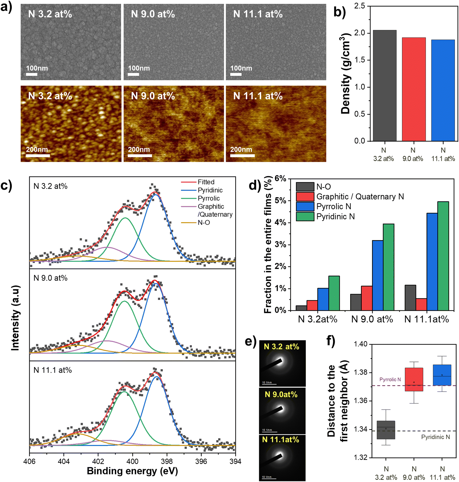 | ||
| Fig. 1 Characteristics of nitrogen-doped amorphous carbon films fabricated with the DC sputtering method. (a) Surface images of the nitrogen-doped carbon films observed with SEM and AFM. (b) Densities of the nitrogen-doped amorphous carbon films acquired with XRR. (c and d) Deconvolution (c) and corresponding quantified ratios (d) of the N 1s spectra of the nitrogen-doped amorphous carbon films. The obtained ratios were calculated using the amount of nitrogen in the amorphous carbon films determined from the XPS results (ESI Fig. S2(a)†). (e) Diffraction patterns of the nitrogen-doped amorphous carbon films. (f) Average distance to the first neighbor for the nitrogen-doped carbon films calculated through the RDF. | ||
Based on the XPS scan results for the nitrogen-doped amorphous carbon films (ESI Fig. S2(a)†), the different amorphous carbon films were fabricated with Ar:N2 = 67:0 contained 3.2 at% nitrogen, Ar:N2 = 60:7 contained 9.0 at% nitrogen, and Ar:N2 = 53:14 contained 11.1 at% nitrogen; for readability, we named these three kinds of nitrogen-doped films N 3.2 at%, N 9.0 at%, and N 11.1 at%, respectively, according to the amount of nitrogen in the films. Although we did not inject nitrogen gas when preparing the Ar:N2 = 67:0 sample, a small amount of nitrogen was present in the amorphous carbon film. This is thought to be due to the small amount of air inherently present in the chamber, which is also the reason why the oxygen was detected in all samples.
Fig. 1(a) shows the typical surface morphologies of the N 3.2 at%, N 9.0 at%, and N 11.1 at% samples observed with FE-SEM and AFM (top and bottom rows, respectively). Overall, the surfaces of the nitrogen-doped amorphous carbon films were smooth with a granular morphology, and the roughness decreased as the amount of nitrogen in the amorphous carbon film increased; the RMS value of the surface roughness of the N 3.2 at% sample was 1.45 nm, and those of the N 9.0 at% and N 11.1 at% samples were 0.22 nm and 0.21 nm, respectively. As the number of nitrogen increases, the surface of nitrogen-doped carbon films becomes smooth because the more nitrogen–carbon bonding is present in a doped carbon thin film, the more vulnerable the film is to plasma bombardment during sputtering deposition.20 The development of a smooth surface due to nitrogen doping is closely related to the density of the nitrogen-doped amorphous carbon film. We measured the density of the nitrogen-doped amorphous carbon films through XRR, and we determined that there was a difference in density according to the nitrogen concentration. As shown in Fig. 1(b), the N 3.2 at% sample showed a density of approximately 2.05 g cm−3, and as the nitrogen content increased, the density of the amorphous carbon film gradually decreased to 1.97 g cm−3 (N 9.0 at%) and 1.88 g cm−3 (N 11.1 at%). Notably, the density of the amorphous carbon thin film decreased even when nitrogen, which is heavier than carbon, was added. It has been reported that the density of amorphous carbon thin films decreases due to nitrogen doping in various deposition methods, such as sputtering,24 filtered cathodic vacuum arc (FCVA) deposition,25 and CVD.26–30 The previous studies have reported that since C–N bonds are much more vulnerable than C–C bonds to damage by plasma in the chamber, the higher the nitrogen concentration is, the more C–N bonds are broken by plasma, thereby lowering the density of the amorphous carbon film; this mechanism is consistent with the reason for increased surface smoothness when nitrogen is added to amorphous carbon films by chemical sputtering effect.23,24 Therefore, considering the changes in surface and density in the nitrogen-doped amorphous carbon films to nitrogen concentration, we found that the physical structure of the carbon thin film deteriorated as nitrogen was added. It should be noted that our nitrogen-doped amorphous carbon made by the DC sputtering process is denser than nitrogen-doped amorphous carbon made by the PE-CVD process.11,17 This means that amorphous carbon thin films made by the DC sputtering process are expected to be effective in manufacturing the excellent hardmasks, because they contain less hydrogen than carbon thin films made by the PE-CVD process.
The properties of a material are closely related to its bonding structure. Therefore, the position of nitrogen in a nitrogen-doped amorphous carbon film is as important as the amount of nitrogen since the position of nitrogen affects the bonding structure of the film. Thus, we performed XPS analysis on the N 1s peaks of the nitrogen-doped amorphous carbon films, which describe the variation in nitrogen more clearly than the C 1s and O 1s peaks (see the ESI†). In the N 1s peak, there are three types of nitrogen bonds associated with carbon: pyridinic (397 to 399.5 eV), pyrrolic (400.2 to 400.9 eV), and graphitic (401 to 403 eV) bonds.31 Pyridinic nitrogen is located at the edge of the hexagonal structure and maintains the hexagonal structure by contributing one pi electron to the aromatic pi system. Pyrrolic nitrogen contributes two pi electrons to the aromatic pi system to destroy the hexagonal structure and forms a pentagonal structure. In contrast, graphitic nitrogen (or quaternary nitrogen) is located at the substitutional site of the hexagonal carbon material structure. As shown in Fig. 1(c), the XPS intensity of the pyrrolic nitrogen component increased as the amount of nitrogen increased, while that of the pyridinic nitrogen component remained consistent and that of the graphitic nitrogen component decreased. In order to intuitively understand how much and what type of carbon–nitrogen bonds are contained in the actual film, we calculated the number fraction of nitrogen in the amorphous carbon films by multiplying the nitrogen ratio according to the bond type confirmed by the deconvolution of the N 1s peak by the nitrogen ratio of the carbon film confirmed by the XPS wide scan, and the result is plotted in Fig. 1(d). As the amount of nitrogen in the amorphous carbon films increased, the amounts of pyridinic nitrogen (1.5% in N 3.2 at%, 3.9% in N 9.0 at%, and 5.0% in N 11.1 at%) and pyrrolic nitrogen (1.0% in N 3.2 at%, 3.2% in N 9.0 at%, 4.4% in N 11.1 at%) increased, showing a linear or higher increase rate depending on nitrogen at%. However, the amount of graphitic nitrogen (0.5% in N 3.2 at%, 1.1% in N 9.0 at%, 0.5% in N 11.1 at%) did not increase linearly with increasing nitrogen at%.
The reason for the increasing amounts of pyrrolic nitrogen and pyridinic nitrogen with an increasing amount of nitrogen in the amorphous carbon films is because the energy required for pyrrolic nitrogen and pyridinic nitrogen bonding is lower than that required for graphitic nitrogen bonding.32 Therefore, an increase in nitrogen ratio with constant energy preferentially forms pyrrolic nitrogen and pyridinic nitrogen, not only during the deposition process but also during the synthesis process.26,33 It should be noted that the fraction of N–O bonding also increased with an increasing amount of nitrogen; however, since both the absolute amount (0.22% in N 3.2 at%, 0.74% in N 9.0 at%, 1.16% in N 11.1 at%) and the change in amount were very small compared to the results for pyrrolic nitrogen and pyridinic nitrogen, we thought that the effect of the N–O ratio on the properties of the carbon thin film would be negligible.
The remarkable increases in pyrrolic and pyridinic nitrogen with the increasing amount of doped nitrogen were also confirmed through TEM analysis. Fig. 1(e) includes the diffraction patterns of the nitrogen-doped amorphous carbon films, clearly showing the amorphous films. We calculated the RDF through Fourier transform of the intensity of the diffraction pattern (ESI Fig. S4†) and derived the distance to the first neighbor. As shown in Fig. 1(f), the average distances to the first neighbor of the N 3.2 at%, N 9.0 at%, and N 11.1 at% samples were 1.34 Å, 1.37 Å, and 1.38 Å, respectively. Also, the bonding lengths of these nitrogen-doped carbon films were similar to those of pyridinic nitrogen (1.32–1.33 Å) and pyrrolic nitrogen (1.372 Å). The distances to the first neighbor in the nitrogen-doped amorphous carbon films are significantly shorter than the bonding lengths of graphitic nitrogen (1.39 Å) or sp3 carbon (1.54 Å) and are closer to the bonding length of sp2 carbon (1.34 Å).34,35 Therefore, it is concluded that the more nitrogen there is in an amorphous carbon film, the more pyrrolic nitrogen there is in the film, which is consistent with the XPS results.
What is the correlation between the increases in the amounts of pyrrolic nitrogen and pyridinic nitrogen as the amount of nitrogen in the carbon thin film increases and the properties of the film? According to previous studies, structural relaxation from an sp3 structure to an sp2 structure occurs in carbon materials as the number of nitrogen increases to relieve the deformation of the carbon structure caused by the introduction of nitrogen.36,37 Additionally, pyrrolic nitrogen and pyridinic nitrogen promote sp2 hybridization, and graphitic nitrogen (or quaternary nitrogen) promotes sp3 hybridization.38,39 Therefore, one can infer that the increases in pyrrolic nitrogen and pyridinic nitrogen with increasing nitrogen amount made the amorphous carbon thin films more closely resemble an sp2 structure. The RDF calculation results that the length of the first neighbor in the nitrogen-doped carbon thin films is much closer to that of sp2 carbon than that of sp3 carbon, as well as the observed decrease in density with increasing nitrogen — sp2 carbon has a lower density than sp3 carbon36 — can also support this inference. If a carbon thin film closely matches an sp2 structure as nitrogen increases, it can be expected that nitrogen doping will deteriorate the etch resistance of the amorphous carbon thin film, which was reported in our previous research.17
3.2. Etching characteristics of nitrogen-doped amorphous carbon films
Following the structural analysis, we determined the etching characteristics of the amorphous carbon thin films according to the amount of nitrogen in the films. The performance of the hardmask was measured with an ICP etcher using CHF3 gas, as shown in Fig. 2(a) and (b). To calculate the selectivity of the amorphous carbon films, we fabricated a dry oxidized SiO2/Si wafer sample (SiO2 thickness: 300 nm) as a reference and deposited the nitrogen-doped amorphous carbon films on the SiO2/Si wafer (Fig. 2(a)). CHF3 is commonly used as an etchant gas for dry etching of Si-based dielectric layers, and we adopted CHF3 gas for etching. The N 3.2 at%, N 9.0 at%, and N 11.1 at% films were etched with a SiO2/Si wafer sample under the same conditions, and the relative etch rate of amorphous carbon was calculated by taking the selectivity of SiO2 etching as 1. Fig. 2(c) shows the thickness of the reference SiO2 and the nitrogen-doped amorphous carbon films before and after etching. While the thickness of SiO2 decreased from 300 nm to 147 nm, those of the nitrogen-doped amorphous carbon films decreased from 112 nm to 57 nm (N 3.2 at%), from 126 nm to 69 nm (N 9.0 at%), and from 130 nm to 73 nm (N 11.1 at%) (ESI Fig. S5†). Based on the results in Fig. 2(c), we calculated the selectivity values of the nitrogen-doped amorphous carbon films, which were 2.76 (N 3.2 at%), 2.71 (N 9.0 at%) and 2.68 (N 11.1 at%), as shown in Fig. 2(d). The selectivity decreased as the nitrogen doping concentration increased, showing as the amount of nitrogen increased, the etching resistance of the amorphous carbon films was reduced. As discussed earlier, the decrease in etching selectivity with increasing nitrogen in amorphous carbon thin films may be due to the decrease in density of the amorphous carbon thin film or the increases in pyrrolic nitrogen and pyridinic nitrogen, which induce hybridization to sp2 carbon with relatively weak etching resistance.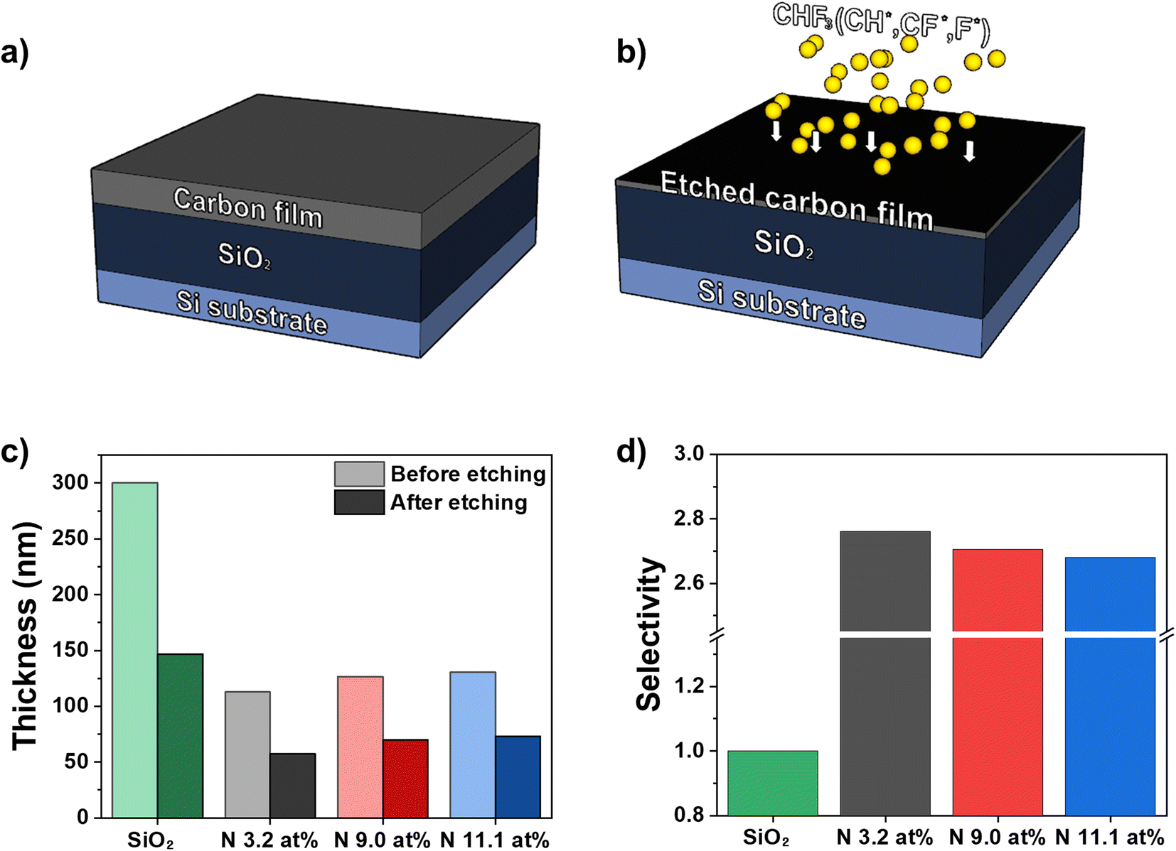 | ||
| Fig. 2 Etching characteristics of amorphous carbon films with different concentrations of nitrogen. (a) Schematic of the sample structure before etching. (b) Schematic of the etching process. (c) Thickness of SiO2 and nitrogen-doped amorphous carbon films before and after etching, as measured from cross-sectional SEM images of the films. The cross-sections of the films were obtained by FIB milling. (d) Selectivity of SiO2 and nitrogen-doped amorphous carbon films. Details of the calculation are described in the Experimental section. | ||
3.3. Effect of nitrogen on fluorine penetration in amorphous carbon films
High resistance to etching caused by physical damage from the plasma source is essential to developing an excellent hardmask. However, the chemical resistance to prevent fluoride ions from penetrating the hardmask is also important. When fluorine ions penetrate through the hardmask, undesired etching could occur upon reaction with the Si-based material under the hardmask or the etch rate of the hardmask could be nonuniform throughout the film.40,41 Therefore, we analyzed the chemical resistance of the amorphous carbon films through TOF-SIMS after etching under the same conditions as we investigated how nitrogen doping affects the penetration of fluorine in the amorphous carbon films. The N 3.2 at%, N 9.0 at%, and N 11.1 at% samples were deposited at 95 nm, 104 nm, and 123 nm, respectively. After etching the three thin films under the same conditions, elemental analysis was carried out according to the final thicknesses of 66 nm, 72 nm, and 91 nm, respectively. Since TOF-SIMS is used to analyze the number of elements in materials by sputtering with Cs, the sputtering time is directly related to the thickness of the film. Based on the relationship between sputtering time and thickness, the penetration depth of F can be calculated from the times at which C- and CF- ions are detected as follows:
Table 1 shows the measured film thicknesses of the nitrogen-doped amorphous carbon films after etching and the times at which C- ions and CF- ions were detected. Fig. 3(a)–(c) are plots obtained by converting the TOF-SIMS profiles of C, F-, CF-, and Si for the N 3.2 at%, N 9.0 at%, and N 11.1 at% films, respectively, into thicknesses through calculation. The penetration depth of fluorine in each nitrogen-doped amorphous carbon film, corresponding to the point where the concentration of CF- almost reaches zero, is denoted by a red dashed line in Fig. 3(a)–(c). The calculated penetration depths of fluorine in the nitrogen-doped amorphous carbon films were 10.9 nm (N 3.2 at%), 5.2 nm (N 9.0 at%), and 5.3 nm (N 11.1 at%), as shown in Fig. 3(d). Interestingly, contrary to the etch selectivity, the penetration depth of fluorine decreased as the amount of nitrogen in the amorphous carbon films increased, and a shorter penetration depth implies the penetration difficulty of fluorine to the amorphous carbon film. Therefore, one can infer that the amount of fluorine penetrating a nitrogen-doped amorphous carbon film would be smaller when the amount of nitrogen in the amorphous carbon film is larger leaving the Si-based material less damaged.
| Film thickness after etching (nm) | Time of C- ion detection (s) | Time of CF- ion detection (s) | Penetration depth of F (nm) | |
|---|---|---|---|---|
| N 3.2 at% | 66 | 175 | 29 | 10.9 |
| N 9.0 at% | 72 | 280 | 20 | 5.2 |
| N 11.1 at% | 91 | 375 | 22 | 5.3 |
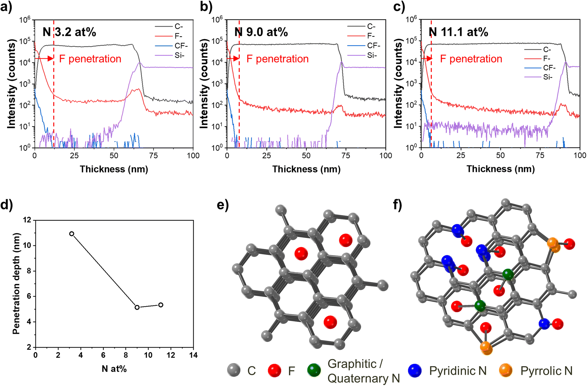 | ||
| Fig. 3 Effect of nitrogen doping on the resistance to fluorine penetration in the amorphous carbon film. TOF-SIMS analysis of the fluorine depth profile of the (a) N 3.2 at%, (b) N 9.0 at% and (c) N 11.1 at% samples. (d) Penetration depth of fluorine in the nitrogen-doped amorphous carbon films acquired based on the TOF-SIMS results. (e and f) Schematic of the behavior of fluorine in carbon materials (e) without nitrogen doping and (f) with nitrogen doping. | ||
Furthermore, the inhibition pathway of fluorine penetration while the amount of nitrogen in an amorphous carbon film is increased was identified. Fig. 3(e) and (f) are schematics of the fluorine behavior in an undoped carbon material (Fig. 3(e)) and a doped carbon material (Fig. 3(f)). If there is no nitrogen, fluorine can penetrate the carbon material by passing between carbons or by transferring bonds with carbons. However, nitrogen from nitrogen doping traps fluorine and hinders fluorine penetration regardless of the nitrogen position (graphitic, pyrrolic, or pyridinic). This is because N–F bonds are much more energetically stable than C–F bonds.40 Therefore, increasing the amount of nitrogen enhances the chemical resistance of the amorphous carbon material, corresponding to previous density functional theory (DFT) results (calculated without considering the location of nitrogen) that the selectivity would be improved by nitrogen doping.15,16,42
4. Conclusion
Nitrogen-doped amorphous carbon films were fabricated through DC magnetron sputtering to produce a semiconductor patterning hardmask. Based on XPS, RDF, and XRR analyses, it was concluded that the amount of nitrogen doping is closely related to the physical and chemical properties of the amorphous carbon film. As the amount of nitrogen increased, the etch selectivity of the amorphous carbon films decreased due to the decrease in the density of the films and the increase in the fractions of pyrrolic and pyridinic nitrogen, which is regarded as the cause of sp2 hybridization. In contrast, the chemical resistance of the amorphous carbon films increased with the increasing amount of nitrogen, as proven by the diminishing penetration depth of fluorine in the films. In designing a superior hardmask, both physical and chemical resistance are important. Based on our findings that the etch selectivity is related to the physical structure of the amorphous carbon film while the chemical resistance is related to the characteristic bonding between nitrogen and fluorine, we suggest that it is possible to improve the etch properties of amorphous carbon films by increasing the density of the film and by placing nitrogen in graphitic positions rather than in pyrrolic and pyridinic positions while increasing the amount of nitrogen in the film since energy transfer to the film could be increased with high ion flux density or plasma power.22,43 This approach would make it possible to fabricate a more reliable hardmask, i.e., a hardmask with a dense structure and high chemical resistance.Conflicts of interest
There are no conflicts to declare.Acknowledgements
This work was supported by the Technology Innovation Program (20011119) funded by the Ministry of Trade, Industry & Energy (MOTIE, Korea). S.-Y. Lee acknowledges the support from a National Research Foundation of Korea Grant funded by the Korean Government (NRF-2018R1A6A1A03025761 and 2021R1G1A1003954).References
- P. Ramm, A. Klumpp, J. Weber, N. Lietaer, M. Taklo, W. De Raedt, T. Fritzsch and P. Couderc, 3D integration technology: Status and application development, ESSCIRC 2010 - 36th Eur. Solid State Circuits Conf., 2010, pp. 9–16, DOI:10.1109/ESSCIRC.2010.5619857
.
- S.-K. Park, in Technology Scaling Challenge and Future Prospects of DRAM and NAND Flash Memory, IEEE Int. Mem. Work., IEEE, 2015, pp. 1–4, DOI:10.1109/IMW.2015.7150307
- K. Babich, A. P. Mahorowala, D. R. Medeiros, D. Pfeiffer, K. E. Petrillo, M. Angelopoulos, A. Grill, V. Patel, S. Halle, T. A. Brunner, R. Conti, S. D. Allen and R. Wise, Hardmask technology for sub-100 nm lithographic imaging, Adv. Resist Technol. Process. XX, 2003, vol. 5039, p. 152, DOI:10.1117/12.485174
- C.-Y. Ho, X. J. Lin, H. R. Chien and C. Lien, High aspect ratio contact hole etching using relatively transparent amorphous carbon hard mask deposited from propylene, Thin Solid Films, 2010, 518, 6076–6079, DOI:10.1016/j.tsf.2010.06.008
- C.-I. Oh, J.-K. Lee, M.-S. Kim, K.-H. Yoon, H.-S. Cheon, N. Tokareva, J.-Y. Song, J.-S. Kim and T.-W. Chang, in Novel spin-on organic hardmask with high plasma etch resistance, ed. C. L. Henderson, Adv. Resist Mater. Process. Technol. XXV, 2008, p. 69232V, DOI:10.1117/12.771758
- J. Robertson, Diamond-like amorphous carbon, Mater. Sci. Eng., R, 2002, 37, 129–281, DOI:10.1016/S0927-796X(02)00005-0
- M. Weiler, S. Sattel, T. Giessen, K. Jung, H. Ehrhardt, V. S. Veerasamy and J. Robertson, Preparation and properties of highly tetrahedral hydrogenated amorphous carbon, Phys. Rev. B: Condens. Matter Mater. Phys., 1996, 53, 1594–1608, DOI:10.1103/PhysRevB.53.1594
- S. Neuville, New application perspective for tetrahedral amorphous carbon coatings, QScience Connect, 2014, vol. 2014, DOI:10.5339/connect.2014.8
- Y. Xiao, X. Tan, L. Jiang, T. Xiao, P. Xiang and W. Yan, The effect of radio frequency power on the structural and optical properties of a-C:H films prepared by PECVD, J. Mater. Res., 2017, 32, 1231–1238, DOI:10.1557/jmr.2016.522
- W. Liu, D. Mui, T. Lill, M. D. Wang, C. Bencher, M. Kwan, W. Yeh, T. Ebihara and T. Oga, in Generating sub-30-nm polysilicon gates using PECVD amorphous carbon as hardmask and anti-reflective coating, ed. A. Yen, Opt. Microlithogr. XVI, 2003, p. 841. DOI:10.1117/12.485532
- S. J. Park, D. Kim, S. Lee, Y. Ha, M. Lim and K. Kim, Diamond-like amorphous carbon layer film by an inductively coupled plasma system for next generation etching hard mask, Thin Solid Films, 2018, 663, 21–24, DOI:10.1016/j.tsf.2018.08.007
- G. Lee, D. K. Sohn, S. H. Seok and H. S. Ko, The effect of hole density variation in the PECVD reactor showerhead on the deposition of amorphous carbon layer, Vacuum, 2019, 163, 37–44, DOI:10.1016/j.vacuum.2019.02.009
- D. Kim, T. T. Kim, S. H. Park, S. K. Lim, H.-C. Lee, T. T. Kim and S.-W. Kang, Characterization of particle generated during plasma-enhanced chemical vapor deposition on amorphous carbon layer using particle beam mass spectrometer, J. Vac. Sci. Technol., A, 2018, 36, 021506, DOI:10.1116/1.5000087
- G. A. Antonelli, S. Reddy, P. Subramonium, J. Henri, J. Sims, J. O’loughlin, N. Shamma, D. Schlosser, T. Mountsier, W. Guo and H. Sawin, Patterning with Amorphous Carbon Thin Films, ECS Trans., 2011, 701–716, DOI:10.1149/1.3572314
- H. Park, S. Lee, H. J. Kim, D. Woo, S. J. Park, J. M. Lee, E. Yoon and G.-D. Lee, Effects of nitrogen doping in amorphous carbon layers on the diffusion of fluorine atoms: A first-principles study, J. Appl. Phys., 2019, 125, 155701, DOI:10.1063/1.5064437
- H. Park, D. Woo, J. M. Lee, S. J. Park, S. Lee, H. J. Kim, E. Yoon and G.-D. Lee, First principles investigation on energetics, structure, and mechanical properties of amorphous carbon films doped with B, N, and Cl, Sci. Rep., 2019, 9, 18961, DOI:10.1038/s41598-019-55488-x
- S.-Y. Lee, K.-T. Jang, M.-W. Jeong, S. Kim, H. Park, K. Kim, G.-D. Lee, M. Kim and Y.-C. Joo, Bonding structure and etching characteristics of amorphous carbon for a hardmask deposited by DC sputtering, Carbon, 2019, 154, 277–284, DOI:10.1016/j.carbon.2019.08.013
- M. Ayiania, M. Smith, A. J. R. Hensley, L. Scudiero, J. S. McEwen and M. Garcia-Perez, Deconvoluting the XPS spectra for nitrogen-doped chars: An analysis from first principles, Carbon, 2020, 162, 528–544, DOI:10.1016/j.carbon.2020.02.065
- X. Mu, D. Wang, T. Feng and C. Kübel, Radial distribution function imaging by STEM diffraction: Phase mapping and analysis of heterogeneous nanostructured glasses, Ultramicroscopy, 2016, 168, 1–6, DOI:10.1016/j.ultramic.2016.05.009
- D. J. H. Cockayne and D. R. McKenzie, Electron diffraction analysis of polycrystalline and amorphous thin films, Acta Crystallogr., Sect. A: Found. Crystallogr., 1988, 44, 870–878, DOI:10.1107/S0108767388004957
- F.-R. Weber and H. Oechsner, Properties of carbon nitride layers generated by direct plasma beam deposition, Surf. Coat. Technol., 1995, 74–75, 704–709, DOI:10.1016/0257-8972(95)08269-7
- N. Hellgren, M. P. Johansson, E. Broitman, P. Sandström, L. Hultman and J. E. Sundgren, Effect of chemical sputtering on the growth and structural evolution of magnetron sputtered CNx thin films, Thin Solid Films, 2001, 382, 146–152, DOI:10.1016/S0040-6090(00)01690-4
- N. A. Morrison, S. E. Rodil, J. Robertson and W. I. Milne, Chemical sputtering of ta-C: Implications for the deposition of carbon nitride, J. Appl. Phys., 2001, 89, 5754–5759, DOI:10.1063/1.1359170
- Y. Togashi, Y. Hirohata and T. Hino, Characterization of CNx films prepared by reactive magnetron sputtering, Vacuum, 2002, 66, 391–395, DOI:10.1016/S0042-207X(02)00160-4
- Y. Iijima, T. Harigai, R. Isono, T. Imai, Y. Suda, H. Takikawa, M. Kamiya, M. Taki, Y. Hasegawa, N. Tsuji, S. Kaneko, S. Kunitsugu, H. Habuchi, S. Kiyohara, M. Ito, S. Yick, A. Bendavid and P. Martin, Fabrication of nitrogen-containing diamond-like carbon film by filtered arc deposition as conductive hard-coating film, Jpn. J. Appl. Phys., 2018, 57, 1–5, DOI:10.7567/JJAP.57.01AE07
- Z. Zhai, H. Shen, J. Chen, X. Li and Y. Jiang, Direct growth of nitrogen-doped graphene films on glass by plasma-assisted hot filament CVD for enhanced electricity generation, J. Mater. Chem. A, 2019, 7, 12038–12049, 10.1039/c9ta01768b
- M. Fenker, J. Julin, K. Petrikowski and A. Richter, Physical and electrical properties of nitrogen-doped hydrogenated amorphous carbon films, Vacuum, 2019, 162, 8–14, DOI:10.1016/j.vacuum.2019.01.018
- B. K. Yen, J. U. Thiele, M. Geisler, P. H. Kasai, R. L. White, B. R. York, H. Zadoori, A. J. Kellock, W. C. Tang, T. W. Wu, M. F. Toney and B. Marchon, Effect of N doping on structure and properties of DLC films produced by plasma beam deposition, IEEE Trans. Magn., 2001, 37, 1786–1788, DOI:10.1109/20.950968
- J. Schwan, V. Batori, S. Ulrich, H. Ehrhardt and S. R. P. Silva, Nitrogen doping of amorphous carbon thin films, J. Appl. Phys., 1998, 84, 2071–2081, DOI:10.1063/1.368268
- S. Rodil, N. A. Morrison, W. I. Milne, J. Robertson, V. Stolojan and D. N. Jayawardane, Deposition of carbon nitride films using an electron cyclotron wave resonance plasma source, Diamond Relat. Mater., 2000, 9, 524–529, DOI:10.1016/S0925-9635(99)00345-3
- L. C. Cheng, T. F. Hung, P. H. Lee, I. C. Lin, H. L. Wen, L. H. Lu, C. L. Chiu, S. C. Chen, J. C. Sung, B. J. Weng and R. S. Liu, Electrochemical reduction of high-efficiency ozone generation through nitrogen-doped diamond-like carbon electrodes, RSC Adv., 2013, 3, 5917–5925, 10.1039/c3ra23335a
- Z. Tian, S. Dai and D. E. Jiang, Stability and Core-Level Signature of Nitrogen Dopants in Carbonaceous Materials, Chem. Mater., 2015, 27, 5775–5781, DOI:10.1021/acs.chemmater.5b02370
- T. Sharifi, F. Nitze, H. R. Barzegar, C. W. Tai, M. Mazurkiewicz, A. Malolepszy, L. Stobinski and T. Wågberg, Nitrogen doped multi walled carbon nanotubes produced by CVD-correlating XPS and Raman spectroscopy for the study of nitrogen inclusion, Carbon, 2012, 50, 3535–3541, DOI:10.1016/j.carbon.2012.03.022
- W. J. Lee, J. Lim and S. O. Kim, Nitrogen Dopants in Carbon Nanomaterials: Defects or a New Opportunity?, Small Methods, 2017, 1, 1–9, DOI:10.1002/smtd.201600014
- J. E. Huheey, E. A. Keiter and R. L. Keiter, Inorganic Chemistry: Principles of Structure and Reactivity, HarperCollins College Publishers, New York, fourth edn, 1993 Search PubMed
- J. Hu, P. Yang and C. M. Lieber, Nitrogen-driven sp3 to sp2 transformation in carbon nitride materials, Phys. Rev. B: Condens. Matter Mater. Phys., 1998, 57, R3185–R3188, DOI:10.1103/PhysRevB.57.R3185
- A. C. Ferrari, S. E. Rodil, J. Robertson, S. E. Rodil and J. Robertson, Interpretation of infrared and Raman spectra of amorphous carbon nitrides, Phys. Rev. B: Condens. Matter Mater. Phys., 2003, 67, 1–20, DOI:10.1103/PhysRevB.67.155306
- W. Ding, Z. Wei, S. Chen, X. Qi, T. Yang, J. Hu, D. Wang, L.-J. Wan, S. F. Alvi and L. Li, Space-Confinement-Induced Synthesis of Pyridinic- and Pyrrolic-Nitrogen-Doped Graphene for the Catalysis of Oxygen Reduction, Angew. Chem., 2013, 125, 11971–11975, DOI:10.1002/ange.201303924
- Y. Nie, X. Xie, S. Chen, W. Ding, X. Qi, Y. Wang, J. Wang, W. Li, Z. Wei and M. Shao, Towards Effective Utilization of Nitrogen-Containing Active Sites: Nitrogen-doped Carbon Layers Wrapped CNTs Electrocatalysts for Superior Oxygen Reduction, Electrochim. Acta, 2016, 187, 153–160, DOI:10.1016/j.electacta.2015.11.011
- D. L. Flamm, C. J. Mogab and E. R. Sklaver, Reaction of fluorine atoms with SiO2, J. Appl. Phys., 1979, 50, 6211–6213, DOI:10.1063/1.325755
- P. Verdonck, A. Goodyear, R. D. Mansano, P. R. J. Barroy, N. St and J. Braithwaite, Importance of fluorine surface diffusion for plasma etching of silicon, J. Vac. Sci. Technol., B: Microelectron. Nanometer Struct., 2002, 20, 791, DOI:10.1116/1.1469015
- T. Kim, D. Kim, Y.-S. Kim, S. H. Park, S. K. Lim, K. O. Park, T. Kim and S.-W. Kang, Strain-controlled boron and nitrogen doping of amorphous carbon layers for hard mask applications, Diamond Relat. Mater., 2016, 69, 102–107, DOI:10.1016/j.diamond.2016.08.002
- M. K. Kuntumalla, M. Attrash, R. Akhvlediani, S. Michaelson and A. Hoffman, Nitrogen bonding, work function and thermal stability of nitrided graphite surface: an in situ XPS, UPS and HREELS study, Appl. Surf. Sci., 2020, 525, 146562, DOI:10.1016/j.apsusc.2020.146562
Footnotes |
| † Electronic supplementary information (ESI) available. See DOI: https://doi.org/10.1039/d2ra06808g |
| ‡ Equally contributed. |
| This journal is © The Royal Society of Chemistry 2023 |