
 Open Access Article
 This Open Access Article is licensed under a Creative Commons Attribution-Non Commercial 3.0 Unported Licence
Arsenene as a promising sensor for the detection of H2S: a first-principles study
Yu-Ping Tian,
Chao-Bo Wang and
Wei-Jiang Gong *
*
College of Sciences, Northeastern University, Shenyang 110819, China. E-mail: gwj@mail.neu.edu.cn
First published on 12th January 2023
Abstract
To explore the feasibility of arsenene in detecting H2S gas, we employ the density-functional theory to investigate the geometry, electronic structure and magnetic properties of defected and doped arsenene. Point defects do not appreciably improve the sensing performance of arsenene due to small adsorption energies and charge transfer. The doping of transition metals (Ti, V, Cr, Mn, Co and Ni) introduces magnetic moments and narrows the band gap of arsenene. Transition metal (TM) dopants can enhance the interaction between H2S and a modified arsenene substrate. Adsorption energies and charge transfers increase significantly, and the adsorption converts to chemisorption. After adsorption, the Ti and Cr-doped system's band gap change is twice that of the pristine and defective arsenene. The adsorption of H2S changes the system properties of two TM-doped arsenenes: Ti-doped arsenene transforms from semiconductor to half-metal, and Ni-doped arsenene transforms from half-metal to conductor. Electrical signals can be observed in this process to detect H2S molecules. Our calculations show that doping improves the detecting performance of arsenene to H2S molecules more efficiently than defects. Our results indicate that arsenene has a promising future in developing H2S gas sensors.
1. Introduction
Hydrogen sulfide (H2S) gas is an inorganic compound, colourless and flammable, widely used in industrial production. It has high neurotoxic potency. Inhalation of small amounts of H2S gas can be lethal. Researchers have recently investigated more and more sensing materials to detect toxic gases.1–3 Two-dimensional (2D) atom-thick materials (graphene,4 germanene,5 silicene,6 phosphorene,7 and antimonene8) are prospective nanometer gas sensors due to their unique characteristics and ultra-high specific surface area.9,10 However, many two-dimensional materials cannot exhibit high sensitivity and selectivity and recover quickly simultaneously. For example, low resistance and a lack of an inherent band gap limit the use of graphene in sensors.11 Perfect graphene has limited application potential because the ordinary gas molecules are physically adsorbed on it.12,13 Materials with adjustable gas-sensitive properties offer the possibility to solve this problem.14Researchers proposed arsenene in 2014,11,15 and its structure is usually buckled or puckered. In addition to high conductivity and low electrical noise, arsenene has a high surface-to-volume ratio. Arsenene can better adsorb some gases16–18 because of the sp3 hybridization and more active adsorption sites provided by the buckled surface structure. It can effectively and selectively interact with gases.19,20 Previous studies have shown that arsenene has a tunable electronic band structure under strain and electric fields.21–23 It has promising potential in 2D nanospintronics devices24 and gas sensing. Like black phosphorus, the carrier mobility of arsenene is as high as several thousand cm2 V−1 S−1.25 This feature enables arsenene to respond quickly when detecting gases. In particular, the physical and chemical properties of arsenene can be regulated effectively by introducing adsorption and doping.26–28 Compared with graphene and silicene, arsenene has lower formation energy and is prone to point defects.29,30 The formation energy of Stone–Wales defects is 1.63 eV and smaller than other typical point defects. The relatively small value causes Stone–Wales defects easy to occur.31,32 Defects and doping modulate the properties of two-dimensional materials to a great extent. According to Wang et al.'s study, the defects in h-BN can exhibit strong defect-photon couping and have exciting properties of photoluminescence (PL) upconversion (anti-Stokes process).33 Tran et al. observed single photon emission in h-BN induced by B vacancy-related defects.34 The magnetic moments of the system can be introduced by vacancy defects.31 The Pt vacancies and Rudeman–Kittel–Kasuya–Yoshida (RKKY) would induce surface magnetism. Therefore, layer-dependent magnetism can be observed.35 Shawkat et al. reported band gap reduction and transitions from semiconductor to metal triggered by Se vacancies in PtSe2.36 Impurities atoms can modify the electronic and magnetic properties of 2D materials. Tullurene can be better employed in spintronic devices because of the contributions of TM dopants to magnetism.37 The doping of O, S and Se in arsenene will behave as metallic characters.38 For blue phosphorene (BP), dopants (Ce, Ti, Ti–Ti) will narrow the band gap.39 V, Cr, and Mn doping in bismuthene can induce magnetic metal, semiconducting and half-metal properties, respectively.40 The magnetic moment values and ground states of TM-doped arsenene differ according to density functional theory (DFT) calculations.27,41,42 Researchers investigated the properties of TM-doped arsenene in two ways: standard DFT and DFT+U. The constant Ueff was set as 2.5 eV for all TM atoms.27,41,42 Employing DFT+U with more accurate Ueff values to investigate the doping of transition metals is necessary. According to a previous report, the adsorption of pristine arsenene to small gas molecules (such as CO, NO, NO2, and NH3) is between physical and chemical adsorption.16,18,43–45 Zhou et al. discovered that TM dopants could improve the interaction between arsenene substrate and HCN molecules more efficiently than defects. Therefore, more research is required to determine how defects and doping affect the sensitivity of arsenene to H2S. Because in previous studies, the DFT method is relatively consistent with the experimental results. We can employ the DFT method to calculate 2D materials' properties.
Our work is mainly divided into the following parts: firstly, we investigate the effects of defects (SW-defects and vacancy) on the sensing performance of arsenene to H2S and compare the best adsorption configuration. Then we further illustrate the effects of H2S on TM-doped systems' magnetic and electronic properties. Our calculations find that TM doping is more effective in improving the sensing performance of arsenene to H2S than defects. The increased adsorption energy and charge transfer between the TM-doped arsenene and H2S molecules indicate stronger interactions. We hope that this work could help develop arsenene-based H2S gas sensors.
2. Computational methods
This paper performs first-principles calculations with the help of spin-polarised density functional theory (DFT), which is implemented in the Vienna Ab initio Simulation Package (VASP).46,47 The projected augmented wave (PAW) pseudopotential49 is used to model the electron–ion interaction. To describe the exchange–correlation energy between electrons, we use the generalized gradient approximation (GGA) of the PBE functional.48 Next, we optimize the structure until the system's total energy achieves an accuracy of 10−6 in structural relaxation. The residual forces of atoms are set as 0.02 eV Å−1. A 15 Å vacuum layer is set to the perpendicular direction to avoid interactions with neighboring slabs. Furthermore, we employ an 8 × 8 × 1 Monkhorst–Pack k-point sampling and set the kinetic energy cutoff as 500 eV. The D3-Grimme correction (DFT-D3)50 is used to consider the weak vdW interaction. A 4 × 4 × 1 β-As supercell containing 32 As atoms is employed to model the arsenene monolayer.Considering the electron correlation effects of the localized 3d orbitals, we add the Hubbard-U parameters to the energy functional of GGA.51 Referring to previous DFT+U research52–54 and our calculation details, the reasonable values of Ueff = U − J for Ti, V, Cr, Mn, Co and Ni atoms are set to 2.5, 3.0, 3.55, 3.5, 2.0 and 2.45 eV, respectively.
3. Results and discussions
3.1 H2S adsorbed on pristine and defective arsenene
The first part investigates the effect of point defects on the adsorption properties. Arsenene adopts a buckling structure and considers two common point defects: single vacancy and Stone–Wales. Fig. 1 shows the relaxed structures of perfect arsenene (P-As), single vacancy (SV-As) and Stone–Wales defected arsenene (SW-As). The pristine arsenene's lattice constant is 3.61 Å, and the bond length of the As–As is 2.52 Å, identical to previous calculations.56,57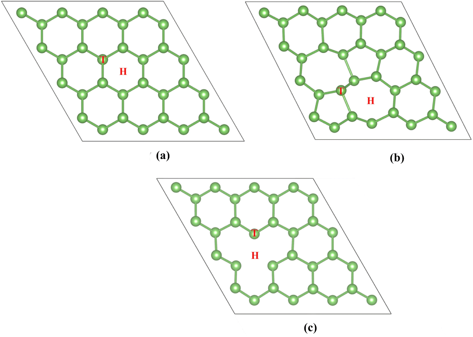 | ||
| Fig. 1 Optimized structures of (a) P-As, (b) SW-As, and (c) SV-As. | ||
Before structure relaxation, we rotate the bond of two neighboring As atoms by 90° to obtain SW-As. We remove an atom from the pristine arsenene and optimize the structure to get the SV defect. After structural optimization, the SW-As system forms the 55–77 structure. The SV defect is centrosymmetric. The three edge atoms of SV-As system are equivalent, and the distance between two edge atoms is 3.53 Å. After introducing point defects, the changes in geometry structure of arsenene are analogous to that of other two-dimensional nanomaterials such as graphene,58 phosphorene,59 and antimonene.60
We calculate the spin-polarized band structures of defected arsenene as depicted in Fig. 2 and 3. As an indirect semiconductor, the P-As system has a band gap of 1.70 eV. The conduct band minimum (CBM) is situated between Γ and M points. The valence band maximum (VBM) is located at the high symmetric Γ points. P-As system's parameters in our calculations are consistent with previous studies.61,62 At the same time, pristine arsenene is a nonmagnetic semiconductor because of its symmetrical band structure. The P-AS system is dynamically stable because its phonon spectrum (plotted in Fig. 2(a)) does not contain imaginary phonon modes.
 | ||
| Fig. 2 (a) Phonon dispersion curves and (b) band structures of P-As. (c) Band structures of SW-As. | ||
 | ||
| Fig. 3 (a) Band structures and (b) top and side views of spin densities of SV-As. The values of isosurface are set to 5 × 10⁻⁷ e Å−3. Yellow and blue colors represent spin-up and spin-down states, respectively. | ||
The defective arsenene loses hexagonal lattice symmetry, and its electronic structure changes. Fig. 2(c) shows that the indirect band gap of SW-As system decreases to 1.48 eV. The CBM moves to Γ point. The charge around the defect localizes strongly due to the flatter band structure. The state in gap (plotted in Fig. 3(a)) appears near the Fermi level because of dangling bonds induced by vacancy defect.
We use the spin-polarized calculation to investigate the magnetic properties of SV-As system. Due to an unpaired electron and dangling bond around the vacancy defect, the SV-As system's total magnetic moment is 1μB. The structure of SV defect is centro-symmetrical, so the spin density is symmetrically localized (plotted in Fig. 3(b)). The electronic properties of perfect arsenene are changed by introducing point defects.
Next, we study the adsorption of H2S on the pristine arsenene and defective arsenene. Obtaining the best adsorption configuration is beneficial to the following study. Considering the geometric structure of arsenene, we set two adsorption sites on the substrate (labelled in Fig. 1): hollow and top sites. Two adsorption models for H2S are considered. One is that the H2S molecule is perpendicular to the substrate, with the S atom close to the surface. The other is H2S molecule parallel to the arsenene substrate. On the whole, we can observe 12 types of initial adsorption configurations. The adsorption energies of H2S molecule on modified arsenene substrate are defined as:
| Eads = EH2S/As − EAs − EH2S | (1) |
Charge analysis can intuitively obtain the electron flow direction after the interaction of each fragment. Moreover, to explore the nature of chemical bonds, we utilize Bader charge analysis55 and calculate the charge density difference (CDD). The definition is defined as follows:
| Δρ = ρH2S/As − ρAs − ρH2S | (2) |
After complete structure optimization, we summarize the corresponding parameters in Table 1. The variation of adsorption energy (Eads) is from −0.107 eV to −0.250 eV. It indicates that H2S molecules weakly interact with arsenene substrates. Bader charge analysis obtains the charge transfer (Q) (0.012e to 0.063e) between the arsenene substrate and H2S molecule. The positive values of Q indicated that H2S molecules obtained charge as the acceptor.
| System | Site | d (Å) | Q (e) | Eads (eV) | |
|---|---|---|---|---|---|
| P-As | Top | Vertical | 3.88 | 0.016 | −0.107 |
| Parallel | 3.91 | 0.015 | −0.112 | ||
| Hollow | Vertical | 3.72 | 0.033 | −0.161 | |
| Parallel | 3.47 | 0.040 | −0.207 | ||
| SV-As | Top | Vertical | 3.48 | 0.052 | −0.191 |
| Parallel | 3.48 | 0.050 | −0.250 | ||
| Hollow | Vertical | 3.64 | 0.022 | −0.158 | |
| Parallel | 3.75 | 0.012 | −0.154 | ||
| SW-As | Top | Vertical | 3.53 | 0.039 | −0.229 |
| Parallel | 3.54 | 0.063 | −0.233 | ||
| Hollow | Vertical | 3.48 | 0.030 | −0.207 | |
| Parallel | 3.47 | 0.033 | −0.186 | ||
The low Eads and Q values suggest the adsorption by physical force. When H2S molecules are parallel to the top sites of SW-As and SV-As, the adsorption energies are maximum. The parameters in Table 1 show that this is the most stable adsorption structure for SW-As and SV-As. The values of Eads are equal to −0.233 eV (SW-As) and −0.250 eV (SV-As), which are larger than the Eads of P-As (−0.112 eV). After structural optimization, the H2S molecule is placed above the arsenene substrate in an inclined structure. The interaction distance between the H2S molecule and arsenene substrate is relatively long (3.47–3.91 Å) in all adsorption systems. In addition, the charge transfer Q of SW-AS (0.063e) and SV-AS (0.050e) are larger than that of P-AS (0.040e). In conclusion, the introduction of SW- and SV-defects improves the adsorption stability to a certain extent. However, the adsorption is still physisorption.
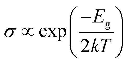
The modulation of H2S adsorption on the electronic band structure of the arsenene system needs further study. The band structures (depicted in Fig. 4) and the density of states (DOS) (plotted in Fig. 5) are calculated by spin-polarized calculations. The band gaps after H2S adsorption decrease by 0.078 eV (P-As), 0.076 eV (SV-As) and 0.044 eV (SW-As), respectively. As shown in Fig. 5, the H2S 2p orbital and As 4p orbital hybridizes near the Fermi level. The band gaps decrease due to the shift of Fermi level after adsorption. Fig. 4(b) illustrates that the degeneracy of two channels at the Γ point vanishes after adsorption. Impurity states arise above the Fermi level due to adsorption. After adsorption, P-As and SW-As are still non-magnetic systems without spin splitting. The magnetic moment of SV-As remained 1μB. The two primary determinants of electrical conductivity, carrier concentration and mobility, are impacted by band gaps. The following equation can define the relationship between band gap and electrical conductivity:
 | (3) |
 | ||
| Fig. 4 Electronic band structures for (a) P-AS, (b) SV-AS, and (c) SW-AS with H2S molecule adsorbed, respectively. The black lines represents spin-up states, and the red lines represents spin-down states. | ||
 | ||
| Fig. 5 Density of states of (a) H2S/P-AS, (b) H2S/SV-AS, and (c) H2S/SW-AS. | ||
3.2 H2S adsorbed on TM-doped arsenene
Due to the limited improvement of arsenene sensing performance by point defects, we introduce transition metal dopants (Ti, V, Cr, Mn, Co, and Ni). TM-doped arsenene is obtained by substituting an As atom from a 4 × 4 × 1 pristine arsenene supercell with a TM atom. Fig. 6 depicts the doped structure after structure relaxation. The geometric deformation is not apparent after structure relaxation.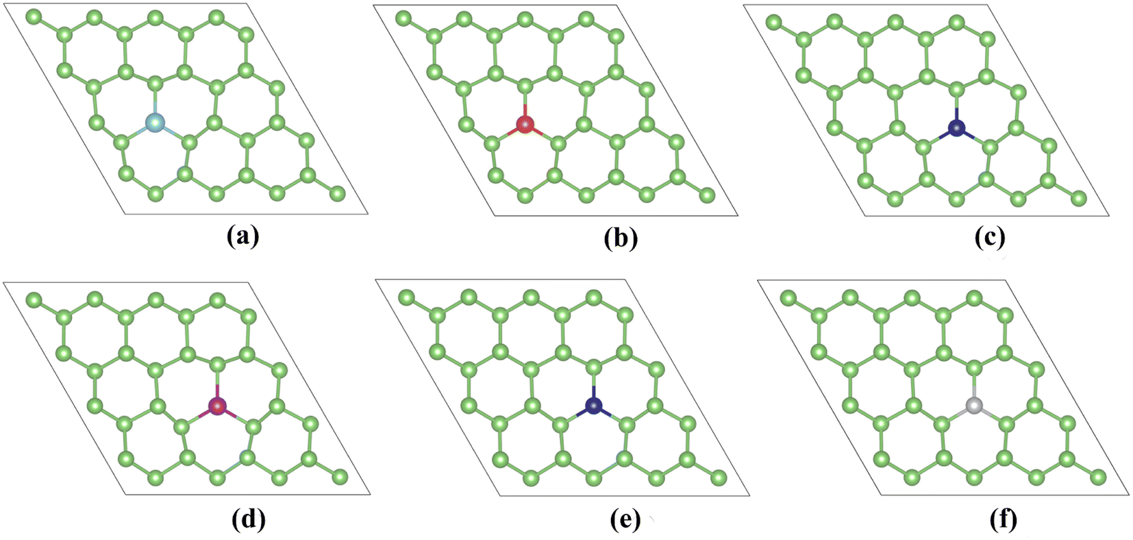 | ||
| Fig. 6 Relaxed structures of (a) TiAs, (b) VAs, (c) CrAs, (d) MnAs, (e) CoAs and (f) NiAs. | ||
After structure optimization, the bond lengths of TM–As (shown in Table 2) for TM-doped arsenene are 2.58 Å (Ti-doped), 2.55 Å (V-doped), 2.56 Å (Cr-doped), 2.56 Å (Mn-doped), 2.37 Å (Co-doped) and 2.31 Å (Ni-doped). The difference in ionic radius from Ti to Ni may result in the variation of the bond lengths of TM–As. Our calculation results are quite different from the GGA results of previous studies.41 The difference may be because strongly correlated systems containing 3d electrons cannot be accurately described by the GGA functional. The stability of TM-doped arsenene can be verified by binding energy (Eb). We can utilize the following equation to calculate the binding energy (Eb):
| Eb = EDoped-As − EV-As − ETM | (4) |
| System | dTM–As (Å) | θ (°) | Eb (eV) | Mtot (μB) | MTM (μB) | MAs (μB) |
|---|---|---|---|---|---|---|
| TiAs | 2.58 | 103.07 | −4.84 | 1.0 | 1.164 | −0.050 |
| VAs | 2.55 | 101.00 | −7.60 | 2.0 | 2.561 | −0.152 |
| CrAs | 2.56 | 100.96 | −3.44 | 3.0 | 4.060 | −0.271 |
| MnAs | 2.56 | 112.23 | −3.67 | 4.0 | 4.648 | −0.170 |
| CoAs | 2.37 | 108.24 | −4.30 | 2.0 | 2.033 | −0.039 |
| NiAs | 2.31 | 103.53 | −4.10 | 1.0 | 0.641 | 0.051 |
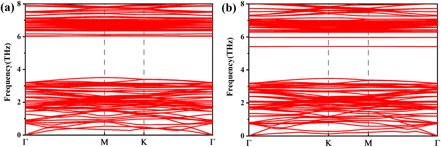 | ||
| Fig. 7 Phonon dispersion curves of (a) TiAs, (b) CrAs. | ||
Differently, the ground state of the Ni-doped system was reported to be non-magnetic by previous studies.41,42,63 The difference in magnetic moments is due to previous studies taken by the GGA functional. This functional will ignore the Coulomb interactions between the localized 3d orbitals. Table 2 shows the antiferromagnetic interactions between TM and the adjacent As atoms in the TiAs, VAs, CrAs, MnAs and CoAs. At the same time, we can observe long-range ferromagnetic interactions between Ni and adjacent As atoms.
The electronic and magnetic properties of arsenene can be influenced by introducing TM dopants. We analyze the electronic band structures (shown in Fig. 8) and density of states (DOS) (depicted in Fig. 10) of doping systems before and after adsorption. The structure of DOS for TM-doped systems is asymmetric. TM impurities can introduce magnetism into arsenene. The corresponding band structure is spin splitting.
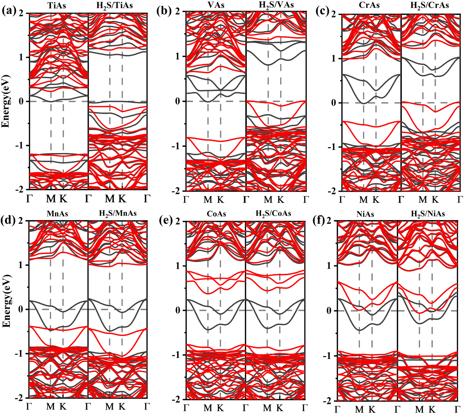 | ||
| Fig. 8 (a)–(f) Electronic band structures for TiAs, VAs, CrAs, MnAs, CoAs and NiAs with and without H2S molecule adsorbed, respectively. The black lines show spin-up band structures, and the red lines represent spin down band structures. | ||
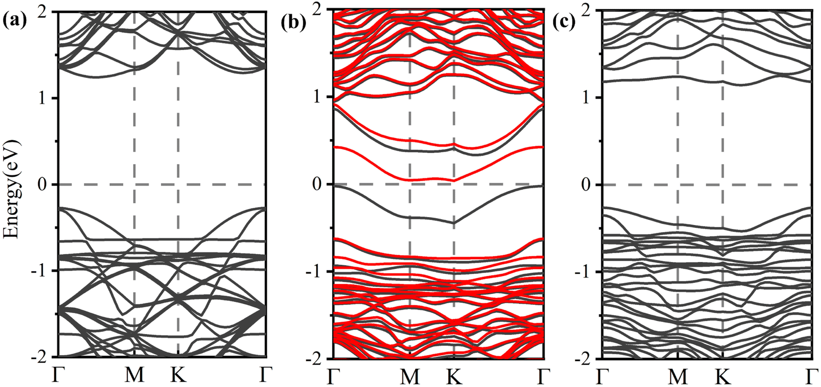
Ti-doped arsenene is an indirect semiconductor (Fig. 8(a)). The majority channels display a band gap of 1.18 eV. The indirect band gap in the minority states is 1.42 eV. The spin-up channels of V-doped arsenene have a direct band gap of 1.12 eV and behave metallic character (Fig. 8(b)). On the contrary, the spin-down channels display an indirect band gap of 1.45 eV and indicate the half-metallic property of the V-doped system. The spin-up channels of MnAs, CoAs and NiAs (see Fig. 8(d)–(f)) show a two-fold degenerate state crossing the Fermi level (EF) and display metallic properties. However, the spin-down channels are semiconducting and indicate the half-metallic behaviors of MnAs, CoAs and NiAs. The CrAs has two majority degenerate channels above the Fermi level. Two minority channels degenerate below the Fermi level. This phenomenon is due to impurity states generated by doping (Fig. 8(c)). The minority states display a direct band gap of 1.41 eV and indicate a half-metallic character. The impurity states near the Fermi level (EF) suggest that VAs, CrAs, MnAs, CoAs and NiAs are spin half-metallic materials. To sum up, TM dopants can effectively regulate the electronic and magnetic properties of arsenene.
The H2S molecules are set parallel to doped arsenene because Table 1 shows that this configuration is the most stable. Besides, the S atom is located above the TM atom, so the influence of TM dopants on adsorption can be considered simultaneously.
We summarize the S–TM bond lengths in Table 3. The bond lengths range from 2.45 Å–2.61 Å. The interaction distance of TM-doped arsenene is shorter than that of pristine and defective arsenene. This suggests a stronger interaction between the H2S molecules and the TM dopants. In addition, the Eads of TM-doped arsenene varies from −0.89 eV to −1.21 eV, effectively enlarged by doping.
| System | Eads (eV) | Q (e) | dS–TM (Å) | Mtot (μB) | MTM (μB) | MH2S (μB) | MAs (μB) | ||
|---|---|---|---|---|---|---|---|---|---|
| As1 | As2 | As3 | |||||||
| TiAs | −1.16 | 0.136 | 2.61 | 1.0 | 1.014 | 0.040 | −0.040 | −0.030 | −0.024 |
| VAs | −1.21 | 0.118 | 2.57 | 2.0 | 2.406 | 0.029 | −0.136 | −0.120 | −0.117 |
| CrAs | −1.01 | 0.168 | 2.57 | 3.0 | 3.859 | 0.028 | −0.257 | −0.255 | −0.202 |
| MnAs | −0.98 | 0.093 | 2.61 | 4.0 | 4.507 | 0.057 | −0.165 | −0.159 | −0.155 |
| CoAs | −1.07 | −0.107 | 2.45 | 2.0 | 1.956 | 0.063 | −0.040 | −0.028 | −0.028 |
| NiAs | −0.89 | −0.101 | 2.53 | 0.7 | 0.468 | 0.011 | 0.044 | 0.040 | 0.028 |
Meanwhile, the charge transfer (Q) of the H2S molecule significantly increases. For Ti, V, Cr and Mn atoms that easily lose electrons, the H2S molecule obtains 0.136e, 0.118e, 0.168e and 0.093e charges from TM-doped arsenene, respectively. For Co and Ni atoms that easily gain electrons, the H2S molecules lose 0.107e and 0.101e charge, respectively. These results show that TM dopants can significantly improve arsenene's sensing performance for detecting H2S molecules. Meanwhile, the adsorption shifts to chemisorption (Fig. 9).
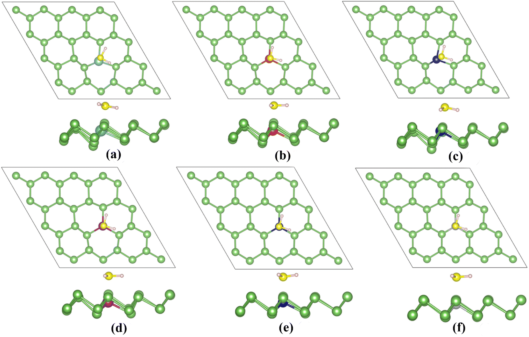 | ||
| Fig. 9 (a)–(f) Relaxed adsorption structures of (a) H2S/TiAs, (b) H2S/VAs, (c) H2S/CrAs, (d) H2S/MnAs, (e) H2S/CoAs and (f) H2S/NiAs. | ||
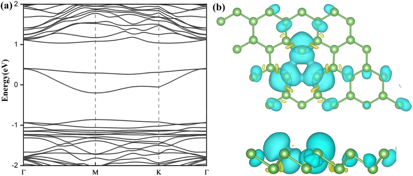
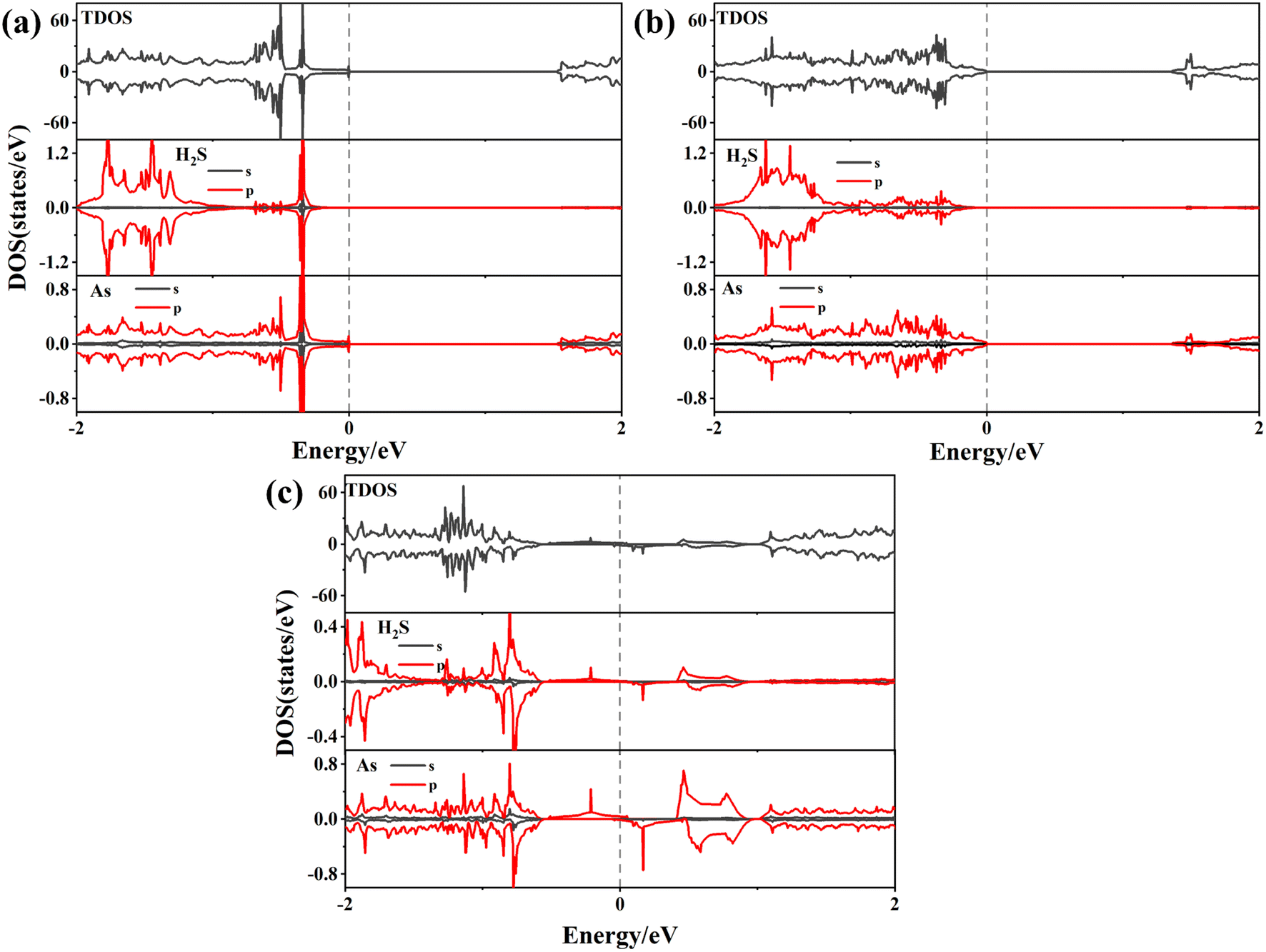
To better understand the detailed changes in the bandgap properties of the TM-doped arsenene after adsorption, the spin-polarized electronic band structures (shown in Fig. 8) and total density of states (TDOS) (depicted in Fig. 10) are calculated. Furthermore, we calculate the projected density of the states (PDOS) of H2S molecules, TM dopant atoms and adjacent As atoms (illustrated in Fig. 11). The Fermi level of Ti-doped system moves down after adsorption (Fig. 10(a)). It makes the system transforms from an n-type doped semiconductor to half metal. The size of band gap of the system decreases. At the Fermi level, the H2S s orbitals hybridize with Ti 3d and As 4p orbitals, which mainly contributes to the band near the Fermi level. At the bottom of the conduction band, the s and p orbitals of H2S hybridize with Ti 3d and As 4p orbitals. After adsorption, the band gap increases, and the Fermi level of V-doped arsenene moves down from CBM to VBM. The half-metallic behaviors of the system remain unchanged. Before adsorption, the Fermi level passes through the majority states. The spin-down band structure is semiconducting. After adsorption, the Fermi level passes through the minority states. The spin-up band structure is semiconducting. The spin-down channels near Fermi level mainly originate from the hybridization of V 3d and As 4p orbitals. The Fermi level (EF) of CrAs moves down, and the size of band gap increases after adsorption. The degeneracy of spin-down channel at Γ before adsorption disappears. The Cr 3d, H2S 3p, and As 4p orbitals hybridize at around 0.5 eV. The hybridization make Fermi level pass through the spin-down channels after adsorption. The band gap of the Mn-doped arsenene is reduced owing to the interactions of H2S 3p, Mn 3d and As 4p orbitals. New spin-down channels appear, but the system is still half-metallic. The Co-doped arsenene remains half-metallic before and after adsorption. The Fermi level passes through two spin-up channels that degenerate at the Γ point before adsorption. After adsorption, the degeneracy disappears and the corresponding density of states increases. Fig. 11 shows that this change is due to the interactions of H2S 3p, Co 3d and As 4p orbitals. After adsorption, the Ni-doped system's band gap decreases, and the system changes from half-metal to conductor. The degeneracy at Γ points disappears after adsorption. Ni 3d and As 4p orbitals mainly contribute to the DOS near the Fermi level. The strong interaction between the dopants and H2S molecules leads to the conversion of physisorption to chemisorption. The band gaps of the system change significantly after adsorption. As shown in eqn (3) above, the electrical conductivity of the system varies greatly. After adsorption, the Ti-doped arsenene changes from semiconductor to half metal, and the Ni-doped arsenene changes from half metal to conductor. The change in electronic properties of the system will generate electrical signals in the substrate We can detect this signal and apply arsenene to sensors.
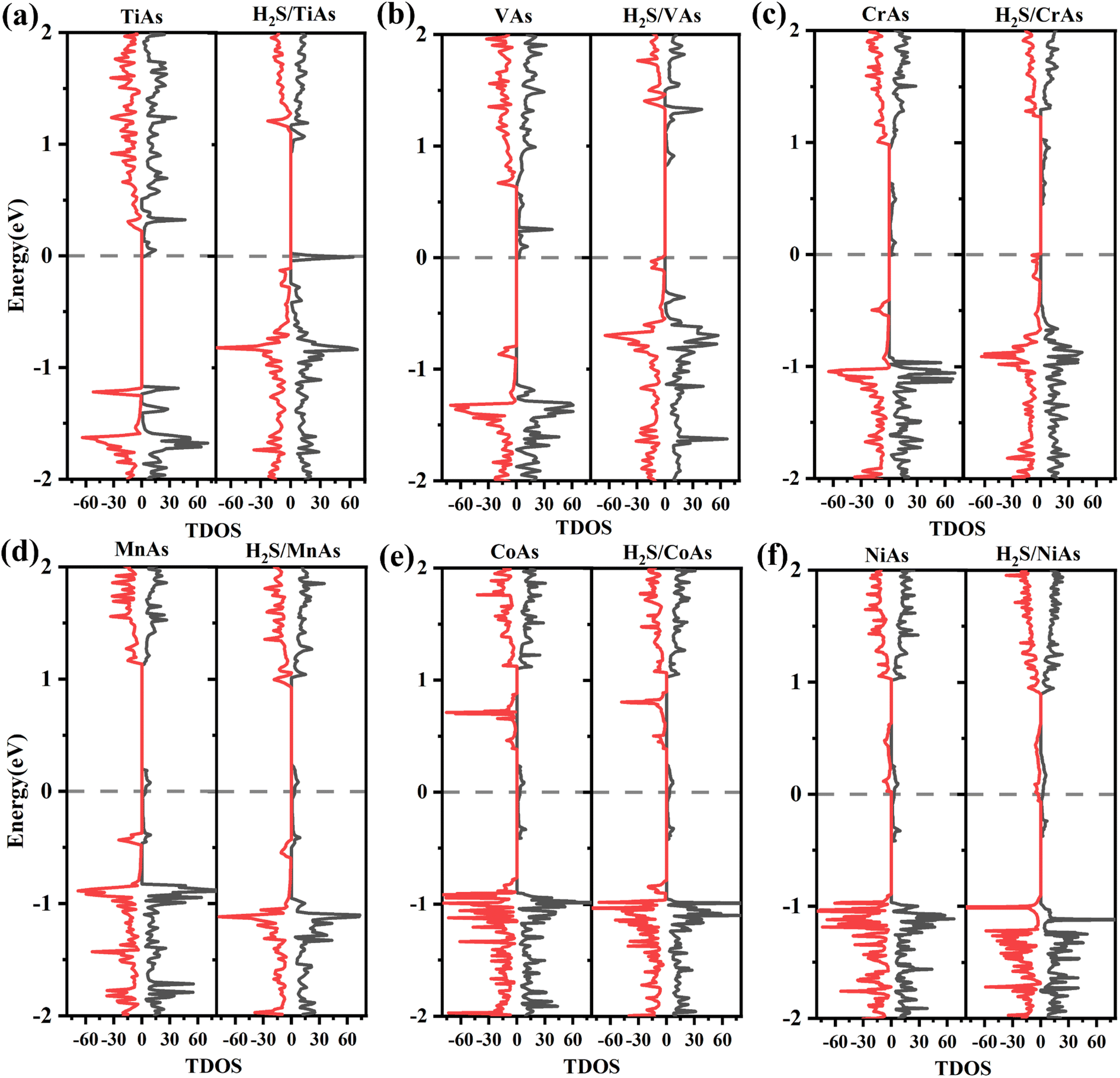 | ||
| Fig. 10 (a)–(f) Spin-polarized density of states (DOS) for TiAs, VAs, CrAs, MnAs, CoAs and NiAs with and without H2S molecule adsorbed, respectively. | ||
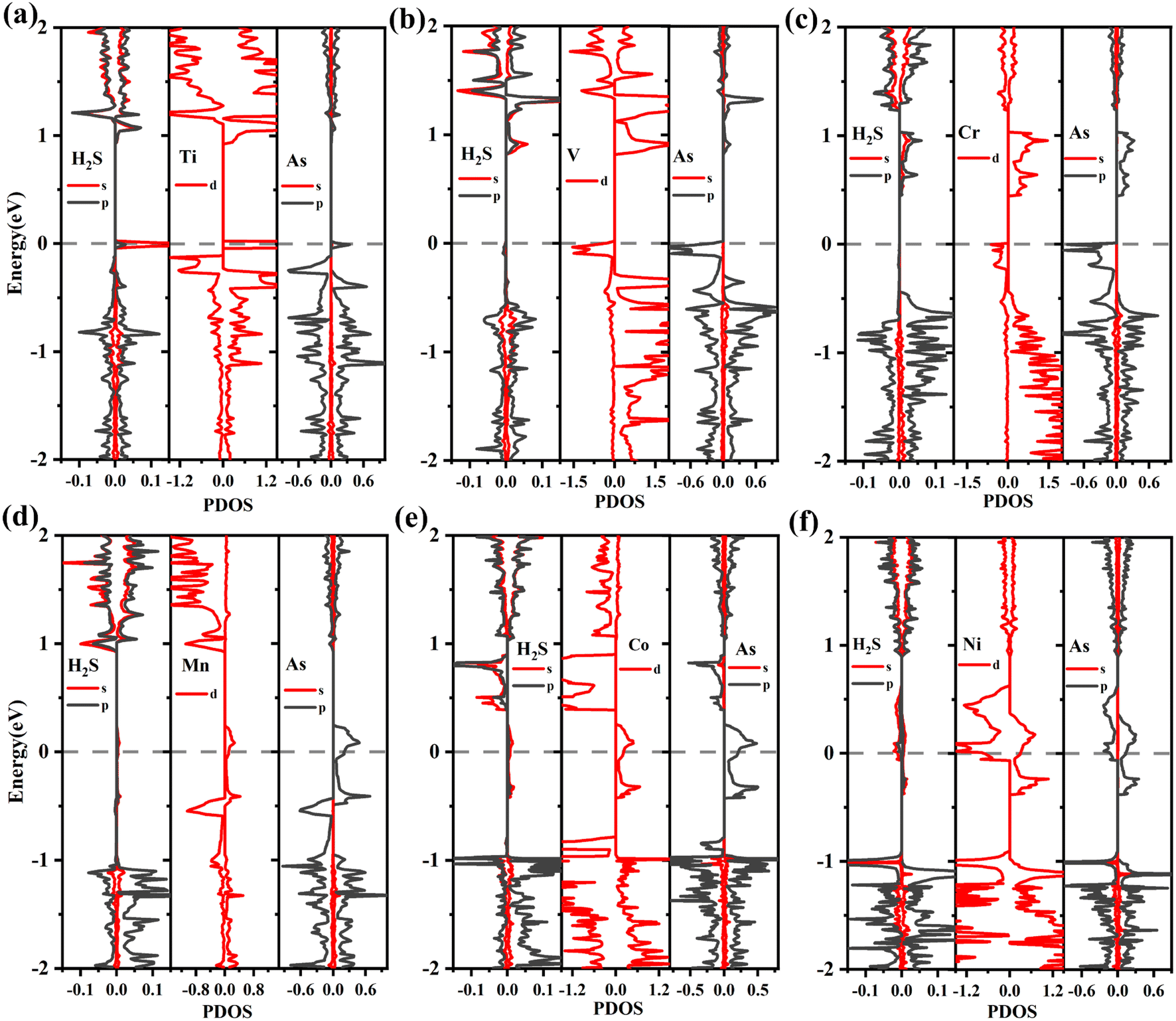 | ||
| Fig. 11 (a)–(f) The PDOS of TM-doped arsenene with H2S adsorbed: (a) H2S/TiAs, (b) H2S/Vas, (c) H2S/CrAs, (d) H2S/MnAs, (e) H2S/CoAs and (f) H2S/NiAs. | ||
The magnetic properties of TM-doped arsenene are affected by H2S adsorption. The magnetization density distribution of TM-doped systems with H2S adsorbed is plotted in Fig. 12. It mainly includes the TM atom, H2S molecule and three surrounding As atoms. Moreover, we calculate the corresponding magnetic moments of TM dopants, H2S molecules and adjacent As atoms. We label the adjacent As atoms as As1, As2, and As3 in Table 3, where As1 has the shortest distance from the TM atom.
 | ||
| Fig. 12 (a)–(f) Top and side views of the spin densities plots of TiAs, VAs, CrAs, MnAs, CoAs and NiAs with H2S adsorbed, where yellow colors represents spin-up states and blue colors represents spin-down states. The isosurface values are set to 0.001 e Å−3. | ||
The ground states of TiAs, VAs, CrAs, MnAs, CoAs and NiAs have magnetism after adsorption. The total magnetic moments are 1.0 (TiAs), 2.0 (VAs), 3.0 (CrAs), 4.0 (MnAs), 2.0 (CoAs) and 0.5μB (NiAs) per supercell. The magnetism of Ni-doped arsenene weakens. The adsorption reduces the Ni-doped system's magnetic moment. As seen in Tables 2 and 3, the contribution of Ni atom and adjacent As atoms to the magnetism of NiAs decreases after adsorption. Other TM-doped systems' total magnetic moments hardly change at all; however, the TM dopant and As atoms' corresponding local magnetic moments decrease. The reduction of local magnetic moment is due to the spin transfer torque. The H2S molecules' local magnetic moments are in the same direction as the TM atom. The TM 3d and adjacent As 4p orbitals mainly contribute to the magnetism (plotted in Fig. 11). Moreover, the asymmetrical structure of H2S molecules' PDOS originates from the hybridization with TM dopant and As atoms.
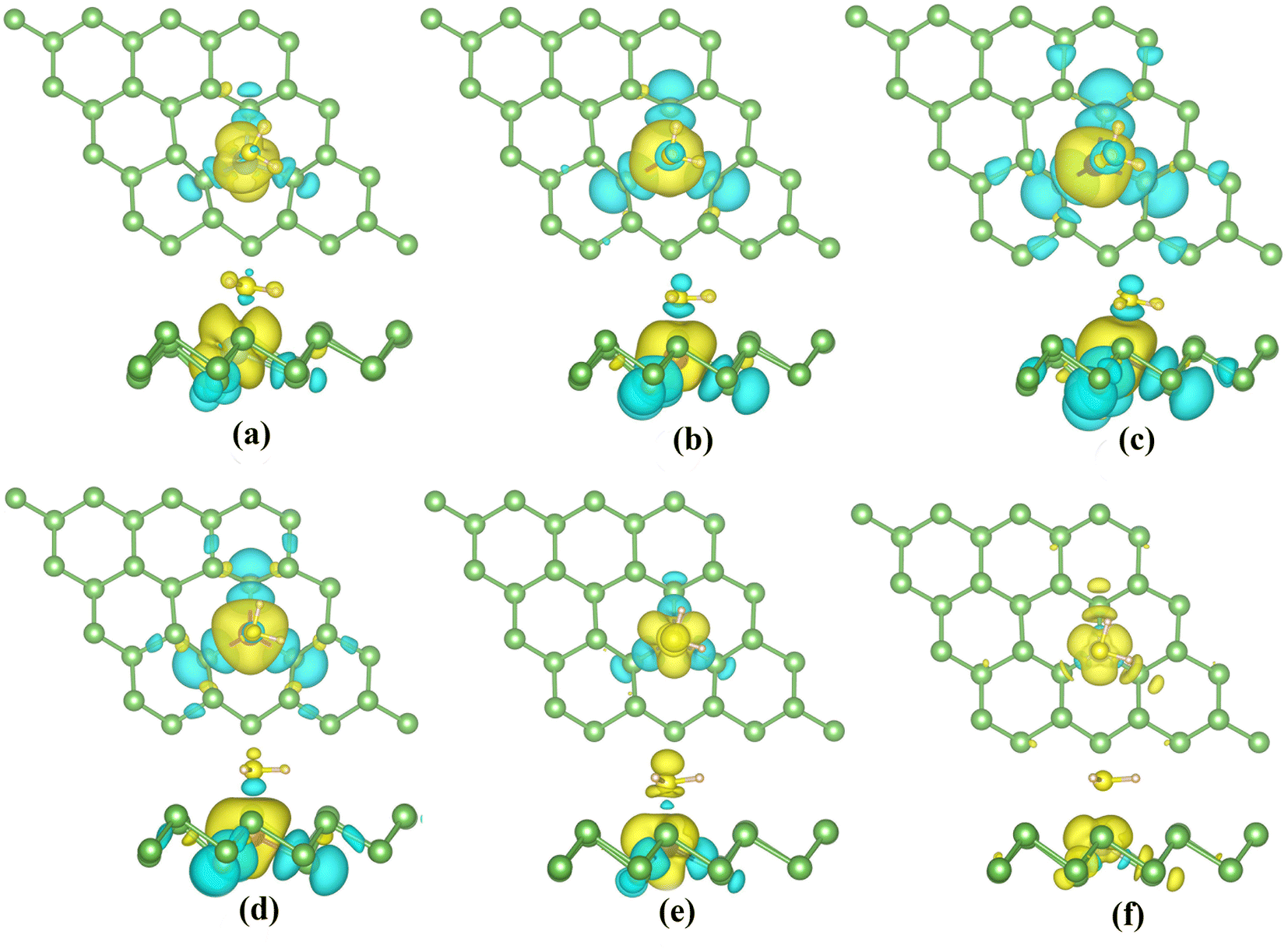
Eventually, we calculate the charge density differences (CDD) (shown in Fig. 13) to understand the charge distribution during adsorption. H2S molecules gain electrons in TiAS, VAs, CrAs and MnAs. The blue region around the TM atoms indicates the loss of electrons. In the case of Co and Ni-doped arsenene, the yellow region around the TM atoms suggests the accumulation of charge. The corresponding H2S molecules lost charge. In addition, the region where electrons converge is concentrated between the H2S molecules and dopant atoms. This aggregation of charge indicates the formation of a covalent bond. In conclusion, strong interactions between the H2S molecules and the TM-doped systems conform to the strong hybridization of the orbitals and the enormous adsorption energy.
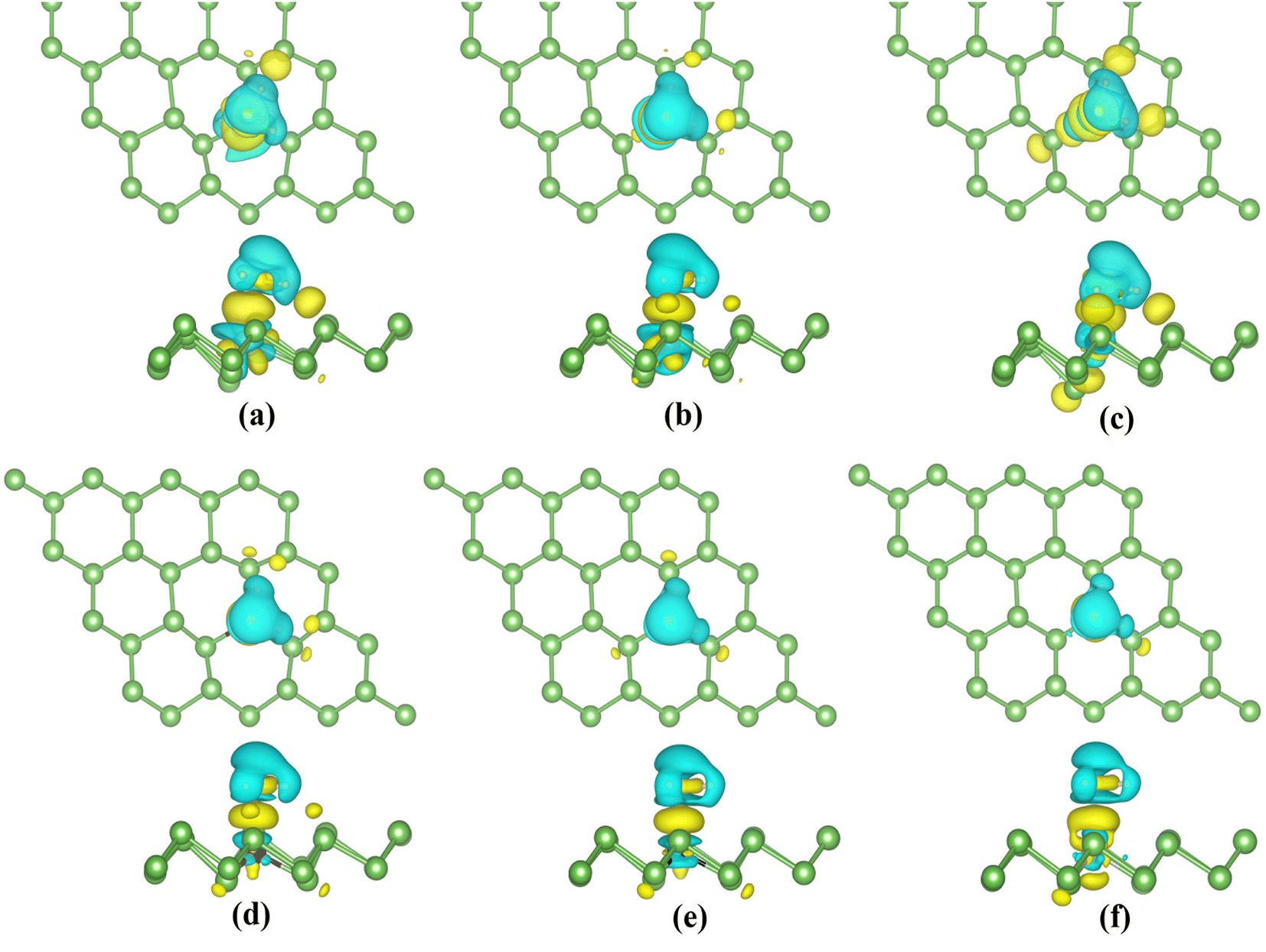 | ||
| Fig. 13 (a)–(f) Top and side views of the charge density differences between H2S molecules and TiAs, VAs, CrAs, MnAs, CoAs and NiAs. Yellow represents the accumulation of charge, and blue represents the diminishing of charge. The isosurface value is set as 0.001 e Å−3. | ||
The introduction of TM dopants makes arsenene have a stronger affinity for H2S molecules. The interactions between arsenene substrate and H2S molecules can be reinforced by TM dopants. In all the doping cases considered, TM-doped arsenene can be employed to detect H2S because of the charge transfer. The cationic of TM renders plural molecules attached to each adsorption site. Therefore, TM-doped arsenene has improved H2S sensing performance significantly. By detecting electrical signals, TM-doped arsenene has a promising application in capturing H2S.
4. Conclusion
In conclusion, we employ first-principles calculations to analyze the feasibility of defective arsenene (SW-As and SV-As) and TM-doped arsenene (TiAs, VAs, CrAs, MnAs, CoAs and NiAs) in detecting H2S molecules. The interaction between arsenene substrate and H2S can be enhanced by introducing SW- and SV-defects. However, the relatively small adsorption energies (−0.107 eV to −0.250 eV) and charge transfer suggest physisorption. After introducing dopants, the sensitivity is effectively improved because adsorption energies (−0.89 eV to −1.21 eV) and charge transfer have significantly increased. The H2S molecules are chemically adsorbed on the TM-doped arsenene. The band gap change of Ti and Cr-doped system after adsorption is 0.1411 eV and 0.1685 eV. The change for the pristine and defective arsenene is less than 0.1 eV. After adsorption, Ti-doped arsenene changes from semiconductor to half-metal, and Ni-doped arsenene transforms from half-metal to conductor. We can observe remarkable electrical signals to detect H2S gas in the adsorption process of TM-doped systems. Therefore, the TM dopants can increase the sensing performance of arsenene to H2S gas more effectively than introducing point defects. Our results suggest that arsenene-based gas sensors have a good application prospect in the future.Conflicts of interest
There are no conflicts to declare.References
- A. Yang, D. Wang, T. Lan, J. Chu, W. Li, J. Pan, Z. Liu, X. Wang and M. Rong, Single ultrathin WO3 nanowire as a superior gas sensor for SO2 and H2S: selective adsorption and distinct I–V response, Mater. Chem. Phys., 2020, 240, 122165 CrossRef CAS.
- W. Li, C. Niu, J. Chu, D. Wang, P. Lv, H. Yuan, A. Yang, X. Wang, Y. Li and M. Rong, DFT+U study of sulfur hexafluoride decomposition components adsorbed on ceria (110) surface, Sens. Actuators, A, 2019, 298, 111590 CrossRef CAS.
- D. Wang, X. Wang, A. Yang, J. Chu, P. Lv, Y. Liu and M. Rong, MoTe2: A Promising Candidate for SF6 Decomposition Gas Sensors With High Sensitivity and Selectivity, IEEE Electron Device Lett., 2018, 39, 292–295 CAS.
- K. S. Novoselov, A. K. Geim, S. V. Morozov, D. Jiang, Y. Zhang, S. V. Dubonos, I. V. Grigorieva and A. A. Firsov, Electric field effect in atomically thin carbon films, Science, 2004, 306, 666–669 CrossRef CAS PubMed.
- A. Kara, H. Enriquez, A. P. Seitsonend, L. C. L. Y. Voone, S. Vizzini, B. Aufrayg and H. Oughaddoub, Corrigendum to “A review on silicene—New candidate for electronics”, Surf. Sci. Rep., 2012, 67, 1–18 CrossRef CAS.
- B. Feng, Z. Ding, S. Meng, Y. G. Yao, X. Y. He, P. Cheng, L. Chen and K. H. Wu, Evidence of Silicene in Honeycomb Structures of Silicon on Ag(111), Nano Lett., 2012, 12, 3507 CrossRef CAS PubMed.
- Y. Cai, Q. Ke, G. Zhang and Y.-W. Zhang, Energetics, Charge Transfer, and Magnetism of Small Molecules Physisorbed on Phosphorene, J. Phys. Chem. C, 2015, 119, 3102–3110 CrossRef CAS.
- S. B. Pillai, S. D. Dabhi and P. K. Jha, Hydrogen evolution reaction and electronic structure calculation of two dimensional bismuth and its alloys, Int. J. Hydrogen Energy, 2018, 43, 21649–21654 CrossRef CAS.
- G. Ko, H. Y. Kim, J. Ahn, Y. M. Park, K. Y. Lee and J. Kim, Graphene-based nitrogen dioxide gas sensors, Curr. Appl. Phys., 2010, 10, 1002–1004 CrossRef.
- J. Park, J. Mun, J. S. Shin and S. W. Kang, Highly sensitive two-dimensional MoS2 gas sensor decorated with Pt nanoparticles, R. Soc. Open Sci., 2018, 5, 181462 CrossRef CAS PubMed.
- S. L. Zhang, Z. Yan, Y. F. Li, Z. F. Chen and H. B. Zeng, Atomically Thin Arsenene and Antimonene: Semimetal–Semiconductor and Indirect–Direct Band-Gap Transitions, Angew. Chem., Int. Ed., 2015, 54, 3112–3115 CrossRef CAS PubMed.
- J. T. Robinson, F. K. Perkins, E. S. Snow, Z. Wei and P. E. Sheehan, Reduced Graphene Oxide Molecular Sensors, Nano Lett., 2008, 8, 3137–3140 CrossRef CAS PubMed.
- B. Huang, Z. Li, Z. Liu, G. Zhou, S. Hao, J. Wu, B. L. Gu and W. Duan, Adsorption of Gas Molecules on Graphene Nanoribbons and Its Implication for Nanoscale Molecule Sensor, J. Phys. Chem. C, 2008, 112, 13442–13446 CrossRef CAS.
- X. Sun, Q. Yang, R. Meng, C. Tan, Q. Liang, J. Jiang, H. Ye and X. Chen, Adsorption of gas molecules on graphene-like InN monolayer: a first-principle study, Appl. Surf. Sci., 2017, 404, 291–299 CrossRef CAS.
- C. Kamal and M. Ezawa, Arsenene: two-dimensional buckled and puckered honeycomb arsenic systems, Phys. Rev. B: Condens. Matter Mater. Phys., 2015, 91, 085423 CrossRef.
- X. P. Chen, L. M. Wang, X. Sun, R. S. Meng, J. Xiao, H. Y. Ye and G. Q. Zhang, Sulfur Dioxide and Nitrogen Dioxide Gas Sensor Based on Arsenene: A First-Principle Study, IEEE Electron Device Lett., 2017, 38, 661–664 CAS.
- R. Bhuvaneswari, V. Nagarajan and R. Chandiramouli, Arsenene nanoribbons for sensing NH3 and PH3 gas molecules – a first-principles perspective, Appl. Surf. Sci., 2019, 469, 173–180 CrossRef CAS.
- M. S. Khan, A. Srivastava and R. Pandey, Electronic properties of a pristine and NH3/NO2 adsorbed buckled arsenene monolayer, RSC Adv., 2016, 6, 72634–72642 RSC.
- Y. Wang, W. Ji, C. Zhang, S. Li, F. Li, P. Li, M. Ren, X. Chen, M. Yuan and P. Wang, Enhanced band gap opening in germanene by organic molecule adsorption, Mater. Chem. Phys., 2016, 173, 379–384 CrossRef CAS.
- W. Hu, N. Xia, X. Wu, Z. Li and J. Yang, Silicene as a highly sensitive molecule sensor for NH3, NO and NO2, Phys. Chem. Chem. Phys., 2014, 16, 6957–6962 RSC.
- H. Cao, Z. Yu and P. Lu, Electronic properties of monolayer and bilayer arsenene under in-plain biaxial strains, Superlattices Microstruct., 2015, 86, 501–507 CrossRef CAS.
- Y. P. Wang, C. W. Zhang, W. X. Ji, R. W. Zhang, P. Li, P.-J. Wang, M. J. Ren, X. L. Chen and M. Yuan, Tunable quantum spin Hall effect via strain in two-dimensional arsenene monolayer, J. Phys. D: Appl. Phys., 2016, 49, 055305 CrossRef.
- H. Zhang, Y. Ma and Z. Chen, Quantum spin hall insulators in strain-modified arsenene, Nanoscale, 2015, 7, 19152–19159 RSC.
- Z. Cui, M. J. Wang, N. Lyu, S. Zhang, Y. C. Ding and K. F. Bai, Electronic, magnetism and optical properties of transition metals adsorbed puckered arsenene, Superlattices Microstruct., 2021, 152, 106852 CrossRef CAS.
- S. Zhang, M. Xie, F. Li, Z. Yan, Y. Li, E. Kan, W. Liu, Z. Chen and H. Zeng, Semiconducting Group 15 Monolayers: A Broad Range of Band Gaps and High Carrier Mobilities, Angew. Chem., Int. Ed., 2016, 128, 1698–1701 CrossRef.
- M. Y. Liu, Y. Huang, Q. Y. Chen, C. Cao and Y. He, Unexpected electronic structure of the alloyed and doped arsenene sheets: first-principles calculations, Sci. Rep., 2016, 6, 29114 CrossRef CAS PubMed.
- J. Du, C. Xia, Y. An, T. Wang and Y. Jia, Tunable electronic structures and magnetism in arsenene nanosheets via transition metal doping, J. Mater. Sci., 2016, 51, 9504–9513 CrossRef CAS.
- M. Bai, W. X. Zhang and C. He, Electronic and magnetic properties of Ga, Ge, P and Sb doped monolayer arsenene, J. Solid State Chem., 2017, 2511–2516 CAS.
- X. Sun, Y. Liu, Z. Song, Y. Li, W. Wang, H. Lin, L. Wang and Y. Li, Structures, mobility and electronic properties of point defects in arsenene, antimonene and an antimony arsenide alloy, J. Mater. Chem. C, 2017, 5, 4159–4166 RSC.
- K. Iordanidou, J. Kioseoglou, V. V. Afanas'Ev, A. Stesmans and M. Houssa, Intrinsic point defects in buckled and puckered arsenene: a first-principles study, Phys. Chem. Chem. Phys., 2017, 19, 9862–9871 RSC.
- X. Liang, S. Ng, N. Ding and C. L. Wu, Characterization of point defects in monolayer arsenene, Appl. Surf. Sci., 2018, 443, 74–82 CrossRef CAS.
- X. Liu, L. Liu, L. Yang, X. Wu and P. K. Chu, Optical Identification of Topological Defect Types in Monolayer Arsenene by First-Principles Calculation, J. Phys. Chem. C, 2016, 120, 24917–24924 CrossRef CAS.
- Q. X. Wang, Q. Zhang, X. X. Zhao, X. Luo, C. P. Y. Wong, J. Y. Wang, D. Y. Wan and T. Venkatesan, et al.) Photoluminescence upconversion by defects in hexagonal boron nitride, Nano Lett., 2018, 18, 6898–6905 CrossRef CAS PubMed.
- T. T. Tran, K. Bray, M. J. Ford, M. Toth and I. Aharonovich, Quantum emission from hexagonal boron nitride monolayers, Nat. Nanotechnol., 2016, 11, 37–41 CrossRef CAS PubMed.
- A. Avsar, A. Ciarrocchi, M. Pizzochero, D. Unuchek, O. V. Yazyev and A. Kis, Defect induced, layer-modulated magnetism in ultrathin metallic PtSe2, Nat. Nanotechnol., 2019, 14, 674–678 CrossRef CAS PubMed.
- M. S. Shawkat, J. Gil, S. S. Han, T. J. Ko, M. J. Wang, D. Dev, J. Kwon, G. H. Lee, K. H. Oh and H. S. Chung, et al.) Thickness independent semiconducting-to-metallic conversion in wafer-scale two-dimensional PtSe2 layers by plasma-driven chalcogen defect engineering, ACS Appl. Mater. Interfaces, 2020, 12, 14341–14351 CrossRef CAS PubMed.
- R. Han, M. Y. Qi, S. J. Dong, Z. Mao, X. Lin and P. Wu, Electronic and magnetic properties of X-doped (X = V, Cr, Mn, and Fe) tellurene for the 2D spintronic device: insights from the first-principles calculations, Phys. E, 2021, 129, 114667 CrossRef CAS.
- Z. W. Liu, X. Li, C. C. Zhou, T. T. Hu, L. Y. Zhang, R. X. Niu, Y. Guan and N. G. Zhang, First-principles study of structural and electronic properties of substitutionally doped arsenene, Phys. E, 2020, 119, 114018 CrossRef CAS.
- R. M. A. Khalil, F. Hussain, M. I. Hussain, A. Parveen, M. Imran, G. Murtaza, M. A. Sattar, A. M. Rana and S. Kim, The investigation of optoelectronic, magnetic and dynamical properties of Ce and Ti doped 2D blue phosphorene: a dispersion corrected DFT study, J. Alloys Compd., 2020, 827, 154255 CrossRef CAS.
- M. Qi, S. Dai and P. Wu, Prediction of electronic and magnetic properties in 3d-transition-metal X-doped bismuthene (X = V, Cr, Mn and Fe), Appl. Surf. Sci., 2019, 486, 58–64 CrossRef CAS.
- M. Sun, S. Wang, Y. Du, J. Yu and W. Tang, Transition metal doped arsenene: a first-principles study, Appl. Surf. Sci., 2016, 389, 594–600 CrossRef CAS.
- J. Du, C. Xia, Y. An, T. Wang and Y. Jia, Tunable electronic structures and magnetism in arsenene nanosheets via transition metal doping, J. Mater. Sci., 2016, 51, 9504–9513 CrossRef CAS.
- M. S. Khan, V. Ranjan and A. Srivastava, NH3 Adsorption on Arsenene: A First Principle Study, IEEE, 2015, pp. 248–251 Search PubMed.
- C. Liu, C. Liu and X. Yan, Arsenene as a promising candidate for NO and NO2 sensor: a first-principles study, Phys. Lett. A, 2017, 381, 1092–1096 CrossRef CAS.
- A. A. Kistanov, Y. Cai, K. Zhou, S. V. Dmitriev and Y. Zhang, Effects of graphene/BN encapsulation, surface functionalization and molecular adsorption on the electronic properties of layered InSe: a first-principles study, Phys. Chem. Chem. Phys., 2018, 20, 12939–12947 RSC.
- G. Kresse and J. Halfer, Ab initio molecular dynamics for open-shell transition metals, Phys. Rev. B: Condens. Matter Mater. Phys., 1993, 48, 13115–13118 CrossRef CAS PubMed.
- G. Kresse and J. Furthmüller, Efficient iterative schemes for ab initio total-energy calculations using a plane-wave basis set, Phys. Rev. B: Condens. Matter Mater. Phys., 1996, 54, 11169–11186 CrossRef CAS PubMed.
- J. P. Perdew, K. Burke and M. Ernzerhof, Generalized Gradient Approximation Made Simple, Phys. Rev. Lett., 1996, 77(18), 3865–3868 CrossRef CAS PubMed.
- G. Kresse and D. Joubert, From ultrasoft pseudopotentials to the projector augmented-wave method, Phys. Rev. B: Condens. Matter Mater. Phys., 1999, 59(3), 1758–1775 CrossRef CAS.
- J. Heyd, G. E. Scuseria and M. Ernzerhof, Hybrid functionals based on a screened Coulomb potential, J. Chem. Phys., 2003, 118, 8207–8215 CrossRef CAS.
- S. L. Dudarev, G. A. Botton, S. Y. Savrasov, C. J. Humphreys and A. P. Sutton, Electron-energy-loss spectra and the structural stability of nickel oxide: an LSDA+U study, Phys. Rev. B: Condens. Matter Mater. Phys., 1998, 57, 1505 CrossRef CAS.
- H. Li, M. Huang and G. Cao, Magnetic properties of atomic 3d transition-metal chains on S-vacancy-line templates of monolayer MoS2: effects of substrate and strain, J. Mater. Chem. C, 2017, 5, 4557 RSC.
- J. He, P. Zhou, N. Jiao, S. Y. Ma, K. W. Zhang, R. Z. Wang and L. Z. Sun, Magnetic Exchange Coupling and Anisotropy of 3d Transition Metal Nanowires on Graphyne, Sci. Rep., 2014, 4, 4014 CrossRef PubMed.
- H. H. Pham, G. T. Barkema and L. Wang, DFT+U studies of Cu doping and p-type compensation in crystalline and amorphous ZnS, Phys. Chem. Chem. Phys., 2015, 17, 26270–26276 RSC.
- W. Tang, E. Sanville and G. Henkelman, A grid-based Bader analysis algorithm without lattice bias, J. Phys.: Condens. Matter, 2009, 21, 084204 CrossRef CAS PubMed.
- M. Y. Liu, Y. Huang, Q. Y. Chen, C. Cao and Y. He, Unexpected electronic structure of the alloyed and doped arsenene sheets: first-principles calculations, Sci. Rep., 2016, 6, 29114 CrossRef CAS PubMed.
- F. Ersan, E. Aktürk and S. Ciraci, Interaction of Adatoms and Molecules with Single-Layer Arsenene Phases, J. Phys. Chem. C, 2016, 120, 14345–14355 CrossRef CAS.
- H. Yildirim, A. Kinaci, Z. J. Zhao, M. K. Y. Chan and J. P. Greeley, First-Principles Analysis of Defect-Mediated Li Adsorption on Graphene, ACS Appl. Mater. Interfaces, 2014, 6, 21141–21150 CrossRef CAS PubMed.
- S. Haldar, S. Mukherjee, F. Ahmed and C. V. Singh, A first principles study of hydrogen storage in lithium decorated defective phosphorene, Int. J. Hydrogen Energy, 2017, 42, 23018–23027 CrossRef CAS.
- S. Dai, W. Zhou, Y. Liu, Y. L. Lu, L. Sun and P. Wu, Tunable electronic and magnetic properties of antimonene system via Fe doping and defect complex: a first-principles perspective, Appl. Surf. Sci., 2018, 448, 281–287 CrossRef CAS.
- A. N. Andriotis, Tunable magnetic properties of transition metal doped MoS2, Phys. Rev. B: Condens. Matter Mater. Phys., 2014, 90, 125304 CrossRef.
- S. Zhang, S. Guo, Z. Chen, et al., Recent progress in 2D group-VA semiconductors: from theory to experiment, 2018 Search PubMed.
- M. Liu, Q. Chen, Y. Huang, C. Cao and Y. He, A first-principles study of transition metal doped arsenene, Superlattices Microstruct., 2016, 100, 131–141 CrossRef CAS.
| This journal is © The Royal Society of Chemistry 2023 |