
 Open Access Article
 This Open Access Article is licensed under a Creative Commons Attribution-Non Commercial 3.0 Unported Licence
Tunable electronic properties and related functional devices for ferroelectric In2Se3/MoSSe van der Waals heterostructures
Y. Zhang ,
X. Q. Deng*,
Q. Jing,
Z. H. Zhang and
X. Ding
,
X. Q. Deng*,
Q. Jing,
Z. H. Zhang and
X. Ding
Hunan Provincial Key Laboratory of Flexible Electronic Materials Genome Engineering, Changsha University of Science and Technology, Changsha 410114, China. E-mail: xq_deng@163.com
First published on 21st December 2022
Abstract
In recent years, two-dimensional (2D) materials have attracted increasing attraction in a number of scientific research fields. In particular, ferroelectric materials with reversible spontaneous electric polarization and Janus transition metal dichalcogenides (TMDs) with intrinsic dipoles exhibit novel properties for many practical applications. Here, the electronic properties of van der Waals (vdW) heterostructures consisting of In2Se3 and MoSSe were investigated based on a first-principles approach. It was demonstrated that four studied In2Se3/MoSSe heterostructures exhibited obvious band gap (Eg) differences, ranging 0.13 to 0.90 eV for PBE (0.47 to 1.50 eV for HSE06) owing to the reversible spontaneous electric polarization of In2Se3 and different intrinsic dipole of MoSSe, and different band alignments of type-I or type-II could also be obtained. The energy bands of the four vdW heterostructures could be obviously regulated by varying degrees of vertical (horizontal) strain and vertical interface electric field, and the Eg varied from zero to 1.27 eV. Then, M4-based mechanical switching devices and ferroelectric diodes were designed based on the significant strain and electric field function. These results provide one possible mechanism for how the polarization direction regulates the physical properties of the system due to the different charges on the two surfaces of the out-of-plane polarized ferroelectric material, which may lead to different proximity effects on the face of the material.
1 Introduction
Since the exploration into graphene in 2004, numerous two-dimensional (2D) materials have been reported,1,2 including h-BN,3 g-C3N4 (ref. 4 and 5) and transition metal dichalcogenides (TMDs).6–8 These 2D materials have the advantages of large surface areas and short carrier migration paths; thus, they have good photocatalytic properties.9–11 Among these materials, TMDs have become one of the most interesting 2D materials in the scientific community because of their novel properties, and they have consequently been applied in many fields, such as energy storage, field effect transistors (FETs), and solar cells. The Janus MoSSe monolayer in TMDs imparts unique electronic and optical properties,12–15 which emerges when the out-of-plane structural symmetry of MoS2 monolayers is broken by chemical vapor deposition.16,17 When one side of the MoS2 monolayer has S atoms replaced by Se, the Janus MoSSe monolayer can be obtained. In terms of its electronic properties, the Janus MoSSe monolayer has built-in electric dipoles due to the broken symmetrical structure.18,19 Optically, it is a material with efficient hydrogen evolution reaction (HER) activity,20 but its oxygen evolution reaction (OER) activity is poor in photocatalytic applications.21 The ferroelectric material In2Se3 is also in the spotlight with unique electronic and optical properties. It has been proved that the ultrathin In2Se3 can form spontaneous polarization as it has a special asymmetric structure according to the existing theoretical calculations and experimental results.22,23 Moreover, In2Se3 can also act as an effective photocatalyst owing to the existence of a built-in electric field, which can separate the different charge carriers.24 However, owing to the existence of a critical thickness effect, reaching a proper thin film is a long-standing challenge. van der Waals (vdW) materials provide a good opportunity for exploring two-dimensional ferroelectric properties as a single atomic layer. A common approach is to construct vdW heterostructures by stacking different 2D monolayers in a specific order, which plays a large role in the combination of various different two-dimensional materials.25–27 The geometry and band structure of the single layer can be protected by the stacked monolayer formed by the extremely weak vdW interactions, on the basis of which there is an opportunity to obtain excellent physical or optical properties that are different from the previous ones.28,29 For example, Wang et al. constructed a vdW heterostructure with two-dimensional Janus MoSSe and black phosphorus monolayers, which could significantly overcome the weak OER activity of the Janus MoSSe and the problem of the excessively fast recombination of generated carriers, thus facilitating the conditions for the spontaneous overall water splitting of black phosphorene/SMoSe heterostructures.30 The two-dimensional GeC/GaN vdW heterostructure demonstrated excellent optical advantages with a suitable band edge position, and an absorption coefficient as high as 105.31 A heterostructure composed by blue phosphorene and ZrSSe monolayers showed a type-I band alignment with an indirect band gap (Eg), and their band alignments could be obviously regulated by the electric field.32In this study, we constructed four vdW heterostructures consisting of In2Se3 and Janus MoSSe monolayers, and defined them as In2Se3/SMoSe(SeMoS) according to the different interfaces between the two monolayers and the electric dipole direction of the In2Se3 monolayer. The results demonstrated that these heterostructures exhibited an obvious Eg difference owing to the reversible spontaneous electric polarization of In2Se3 and different intrinsic dipoles of MoSSe, and also that the electronic properties of the four devices could be regulated by varying the degrees of the vertical (horizontal) strain and the vertical interface electric field, thus proving the design of a mechanical switch device and ferroelectric diode based on the M4 stacking order (see Section 3.1) according to the strain and electric field function.
2 Models and methods
The geometry construction and calculations of the device properties were performed by density functional theory (DFT) using the Atomistix ToolKit software,33 which has been widely employed in simulation studies of low-dimensional materials.34,35 The residual force on each atom was less than 0.01 eV Å−1 and the maximum step size was 0.2 Å for ionic relaxation. The exchange–correlation potential was described through the Perdew–Burke–Ernzerhof (PBE) functional within the generalized gradient approximation (GGA). Because PBE does not account for van der Waals interactions,36–38 we added the empirical dispersion correction DFT-D2 method described by the pairwise force field.38 The temperature in the calculation was set to 300 K and the cutoff energy was 150 Ry, which was required in the numerical integration and solving of the Poisson equation. In order to assess the accuracy, we did a convergence test on the cutoff energy for the monolayer and heterostructure, and the test results showed that when the cutoff energy was greater than 150 Ry, the relative atomic energy would be less than 0.001 eV; that is, the cutoff energy converges. The k-point grid sampling was set as 11 × 11 × 1 for norm conservation of the Troullier–Martins pseudopotential. We set a vacuum layer of length 30 Å in the z-axis direction to avoid the effect of repeated images.3 Results and discussion
3.1 Structure and electronic properties of the In2Se3/MoSSe vdW heterostructures
The supercellular vdW heterostructures consisted of 4 × 4 In2Se3 and MoSSe monolayers, and the lattice constants for the unit cell for In2Se3 (MoSSe) were 4.19 (3.23 Å). We stacked In2Se3 on the MoSSe monolayer vertically to construct the vdW heterostructure, and the lattice parameters of the heterostructure 16.76 Å. There were different surface atoms of MoSSe and different electric dipole orientations of the In2Se3 monolayer. In order to better match the In2Se3 and SeMoS monolayers, the generalized lattice matching (GLM) method was used to balance the relationship between the mismatched strain and atomic number.39,40 Four possible stacking orders of In2Se3/MoSSe were considered, namely M1, M2, M3, and M4. For M1 (M2), the Se (S) atoms of MoSSe faced In2Se3, with the electric dipole of the In2Se3 monolayer pointing upwards, as seen in Fig. 1(a) and (b), defined as M1(In2Se3/SeMoS) and M2(In2Se3/SMoSe), respectively. For M3 (M4), the S (Se) atoms of MoSSe faced In2Se3 with the electric dipole of In2Se3 pointing downwards, defined as M3(SeMoS/In2Se3) and M4(SMoSe/In2Se3) in Fig. 1(c) and (d). The interlayer distances were 3.70, 3.56, 3.64, and 3.58 Å for M1–M4 with the most stable stacking structures, respectively. In the following, we calculate the binding energy of M1–M4, and the formula for the binding energy is: Eb = (EHS − EIn2Se3 − EMoSSe), where EHS, EIn2Se3, and EMoSSe represent the total energy of the heterostructure, In2Se3, and MoSSe monolayer, respectively. If the components of a system are separated to infinity, a certain amount of energy is required to overcome the attraction. The calculated binding energies were −940, −1220, −1310, and −1120 meV for M1–M4. To gain an insight into the nature of the binding energy, based on previous studies,41,42 we calculated the binding energy again using the formula: Eb = EvdW + ESR, where the short-range energy is ESR, as described by the PBE exchange–correlation functional, and the long-range vdW attraction energy is EvdW. For M1–M4, the values of ESR were 75, 108, 130, and 85 meV, and the EvdW values were −1015, −1328, −1440, and −1205 meV. These calculations prove that the formation of these heterostructures were energetically advantageous and were in agreement with the literature.41,42
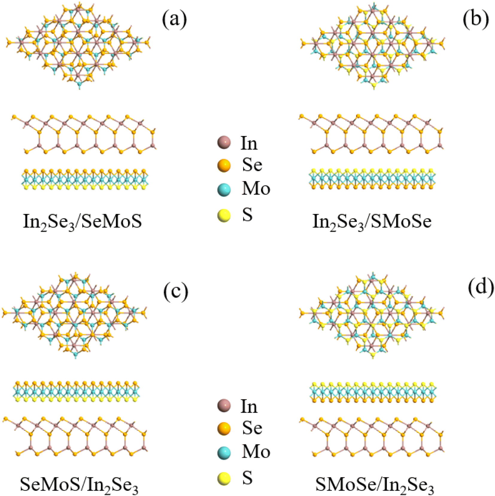 | ||
| Fig. 1 Four In2Se3/MoSSe heterostructures as M1–M4: top and side views of (a) M1, (b) M2 (c) M3, (d) M4. The brown, gold, yellow, and blue represent In, Se, S, and Mo atoms, respectively. | ||
We calculated the energy band structures of the isolated In2Se3 and MoSSe monolayers with PBE (HSE06) calculations, as shown in Fig. 2(a) and (b). It could be seen that the In2Se3 exhibited an indirect Eg with 0.81 eV (1.34 eV), and the conduction band minimum (CBM) was located at the Γ-point, while the valence band maximum (VBM) was located between the Γ- and k-points. For the MoSSe monolayer, both the VBM and CBM were seated at the Γ-points, and the value of the direct Eg was 1.64 eV (2.08 eV), which basically agreed with the theoretical values (0.81 and 1.54 eV).43,44 The energy band structures for M1–M4 with the PBE (HSE06) calculation in Fig. 2(c) and (d), and the values of Eg were 0.87 (1.49), 0.90 (1.50), 0.56 (0.70), and 0.13 eV (0.47 eV). We could see that the band structures calculated by the PBE and HSE06 were basically similar, especially for those around the Fermi level, and the band gap types were exactly the same. The PBE calculation obviously underestimated the band gap size, and thus the HSE06 calculation is generally believed to give more precise results for the band gap of a material. However, there are larger calculation difficulties if the HSE06 is used. Therefore, we only performed PBE calculations rather than HSE06 calculations to reduce the calculation cost for various modulations of the heterostructures and we believe that such an impact on the calculated results was acceptable.
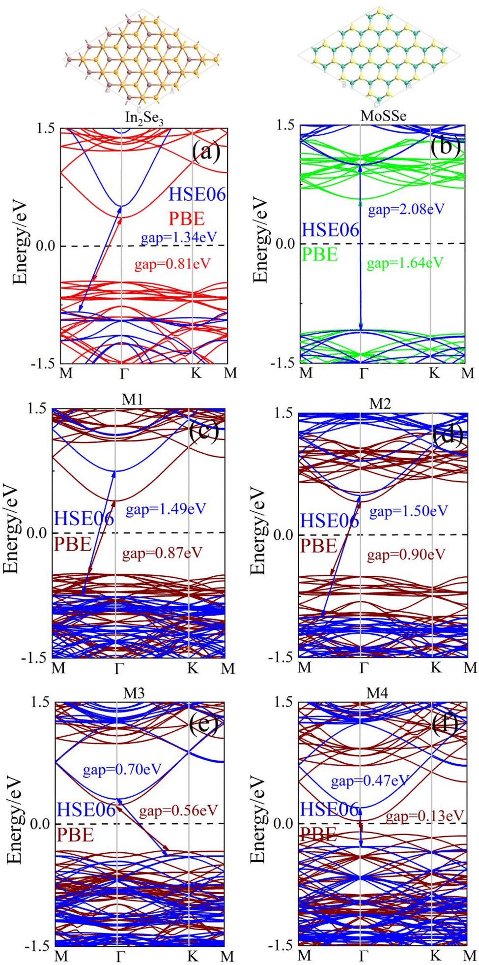 | ||
| Fig. 2 Band structures for (a) In2Se3 monolayer, (b) MoSSe monolayer, (c) M1, (d) M2, (e) M3, and (f) M4 by PBE (HSE06). | ||
Fig. 3 shows the projected band structures (Fig. 3(a), (c), (e) and (g)) and the projected density of states (PDOS) (Fig. (b), (d), (f) and (h)) for the four different M1–M4 systems. As shown in Fig. 3(a), M1 clearly showed a direct Eg of 0.87 eV, with both the CBM and VBM seated at the Γ-points. The PDOS of the M1 heterostructure indicated that the CBM originated from the In2Se3 monolayer, while the VBM was contributed by the In2Se3 and MoSSe monolayers in Fig. 3(b). For M2, which also showed an indirect Eg of 0.90 eV in Fig. 3(c), the CBM (VBM) was also derived from the In2Se3 monolayer, which was a typical type-I band arrangement, as shown in Fig. 3(d). Therefore, two types of charge carriers tend to be transported from MoSSe to In2Se3 due to the band shift, which favors recombining holes and electrons, and so type-I heterostructures have promising applications in light-emitting diodes (LEDs) and lasers.45,46 For M3, it had a direct Eg of 0.56 eV, as seen in Fig. 3(e), and CBM originated from the In2Se3 monolayer, while the VBM was contributed mainly by MoSSe monolayers and a small amount by the In2Se3 monolayer, as seen in Fig. 3(f). While for M4, there was a narrow direct Eg of 0.13 eV, and the VBM was further away from the Fermi level (Ef) than the CBM. Moreover, the conduction and valence bands with a broad energy region originated from the In2Se3 and MoSSe monolayers, respectively. These data indicate a typical arrangement of type-II bands. According to our previous study on the type-II band alignment,47 the electrons in the MoSSe monolayer will move toward the CB of the In2Se3 monolayer, while the holes in the In2Se3 monolayer will shift to the VB of the MoSSe monolayer. This band alignment could effectively separate electrons and holes, and thus could be used in the field of optoelectronic devices.48,49
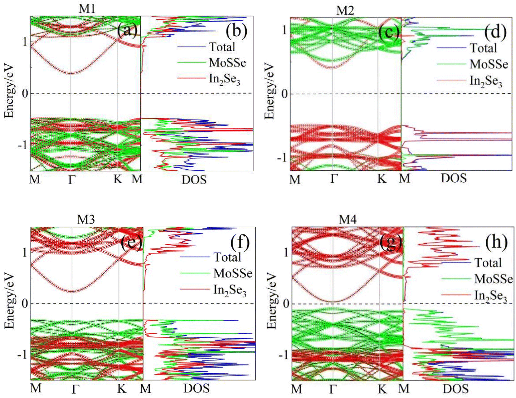 | ||
| Fig. 3 Projected band structures of (a) M1, (c) M2, (e) M3, and (g) M4. Projected density of states (PDOS) of (b) M1, (d) M2, (f) M3, and (h) M4. | ||
From the analysis of the above results, it can be seen that the In2Se3/MoSSe vdW heterostructures have the characteristics of various energy band structures, including a type-I band arrangement and type-II band arrangement. To better understand them, we calculated the charge density difference between M1–M4 to show the charge transfer between In2Se3 and MoSSe, as shown in Fig. 4. It is well known that Janus MoSSe monolayers have an intrinsic layer dipole moment from Se to S atoms in the layer.50 Meanwhile, the In2Se3 monolayer also has upward or downward electric dipoles.51 In addition, a weak dipole moment also existed in the interface region between the S in MoSSe and the Se atomic layers in In2Se3. The plane charge density difference Δρ(Z) calculation formula is  , where ρH(x,y,z), ρIn2Se3(x,y,z), and ρMoSSe(x,y,z) represent the charge densities of the heterostructure, In2Se3, and MoSSe at a certain point (x,y,z), respectively. The positive (Δρ(Z) > 0) and negative values (Δρ(Z) < 0) represent electron accumulation and depletion (hole accumulation). Fig. 4 shows the corresponding isosurfaces for the difference in charge density, and it is clear that the charge was transferred from MoSSe to the In2Se3 monolayer, but the degree of charge transfer was different for the four systems. The electrons and holes accumulate in the In2Se3 and MoSSe region. There was more charge transfer in M2 (M3) than M1 (M4), which originated from the different interfacial effects as well as the BP/MoSSe heterostructures.50
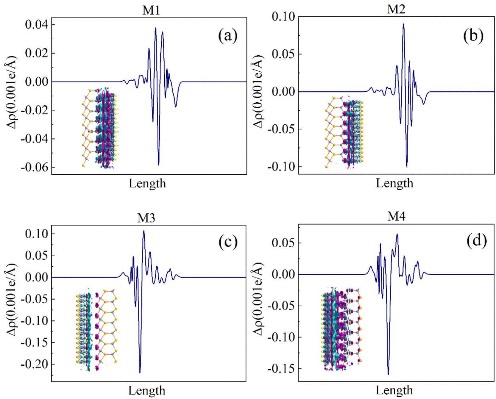 | ||
| Fig. 4 Integrated charge density difference along the direction perpendicular to the interface of (a) M1, (b) M2, (c) M3, and (d) M4. Purple and cyan areas denote electron accumulation and depletion, respectively. | ||
3.2 Vertical strain effects on the In2Se3/MoSSe vdW heterostructures
To explore the regulation of the interlayer distance on the electronic properties affecting the coupling interaction and electron distribution of the interface, we calculated the Eg changes of M1–M4 under a series of vertical strains (ε) from −0.8 Å to +0.8 Å with a step of 2%. Here, ε = d − d0, where d and d0 represent the compressed (stretched) and equilibrium state interlayer distances. A positive (negative) ε corresponds to stretch (compressive) strain in Fig. 5(a) and (b). The Eg of M1–M4 decreased monotonously when applying stretch strain, and there was a transition between a semiconductor and metal for M1 when ε was over 0.6 Å. With the increasing compressive strain, the Eg of M2 (M3) showed a slight increase at first, and then gradually dropped when ε was over 0.4 Å for M3. However, the Eg of M1 and M4 showed a marked increase under compressive strain, and the maximum values reached 1.27 and 0.47 eV, which were about 1.5 and 4 times that of the equilibrium Eg. When ε was over 0.6 Å, the Eg of M4 decreased to zero. Therefore, as shown in Fig. 7(h), an M4-based mechanical switching device could be designed, in which M4 was used as the material for the central diffusion region of the device, and the two electrodes were made of graphene and the metal. When the two electrodes are properly biased, the CBM and VBM enter the bias window to achieve a narrow Eg and a lower potential barrier, allowing the device to be in the “On” state, resulting in a higher current flow. By applying pressure to the heterostructure, the CBM and VBM will exit the bias window, and the higher barrier keeps the device in the “Off” state with negligible current flow. Therefore, a device with a high on/off ratio (Ion/Ioff) can be obtained.52 Once the heterostructure is stretched back to equilibrium, the device returns back to the “On” state.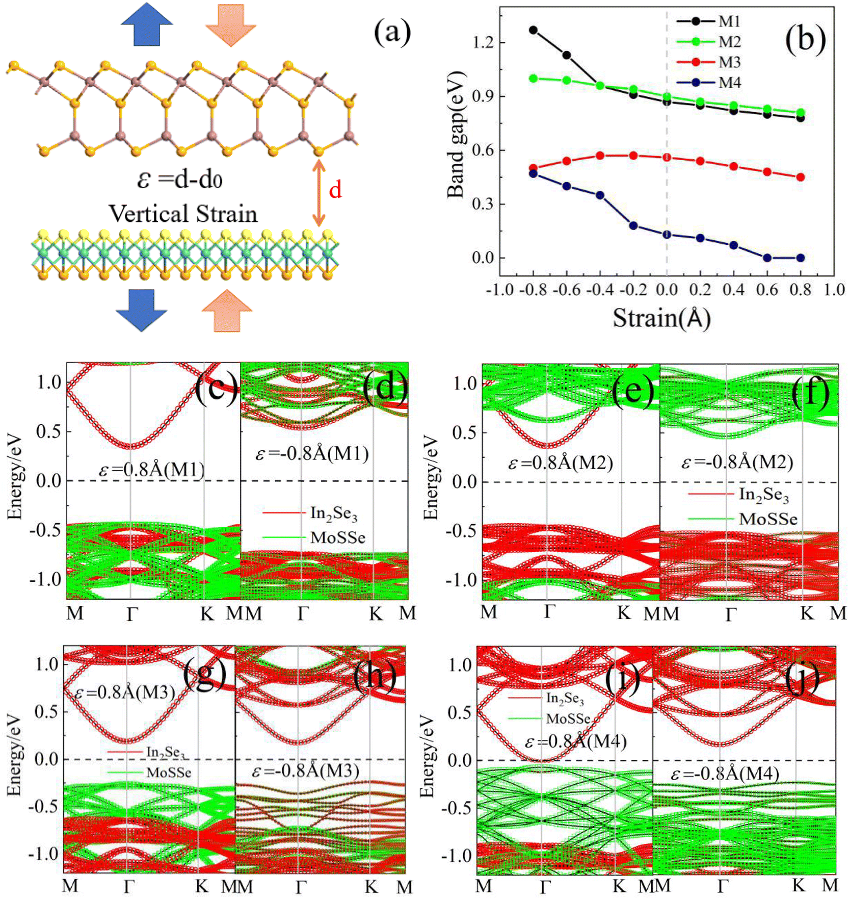 | ||
| Fig. 5 (a) Schematic illustration of the synergistic effects of the vertical strain, (b) Eg as a function of the vertical strain, (c)–(j) projected band structures of the heterostructure under the selected vertical strain of ±0.8 Å. | ||
Fig. 5(c)–(j) show the change in band edge position of M1–M4 under ε = ±0.8 Å, which is conducive to a clear understanding of the physical mechanism of Eg modulation. We can see that the VBM (CBM) of M1 was shifted downwards (upwards) obviously at −0.8 Å compared with 0.8 Å and the equilibrium state, leading to a distinctly increased Eg in Fig. 5(c) and (d). For M2, it still showed a type-I band alignment at 0.8 Å as well as the equilibrium state, and EC-In2Se3 (EC-MoSSe) was shifted upwards (downwards) at −0.8 Å, thus the CBM was contributed by the MoSSe monolayers. Therefore, the transition from a type-II to type-I heterostructure for M2 will be achieved with the vertical strain effect. The VBM showed a little decrease and CBM showed an opposite change compared with 0.8 Å and the equilibrium state, and the Eg was a little augmented, as shown in Fig. 5(e) and (f). For M3, the CBM (VBM) at 0.8 Å and −0.8 Å kept almost the same position, which contributed the In2Se3 monolayer, while the VBM was contributed by the MoSSe (In2Se3) monolayer at 0.8 Å (−0.8 Å), as shown in Fig. 5(g) and (h). Therefore, the Eg of M3 showed only a little change at −0.8 Å and 0.8 Å strain; while the CBM contributed by the MoSSe reached the Fermi level compared with the equilibrium state for M4, and thus the Eg was zero at 0.8 Å, as shown in Fig. 5(i), and the VBM (CBM) of M4 shifted further away from the Fermi level at −0.8 Å, leading to an increased Eg, as shown in Fig. 5(j).
3.3 Horizontal strain effects on In2Se3/MoSSe vdW heterostructures
The horizontal stress application method is also a simple and effective method for tuning the electronic properties of a device.53 Therefore, we investigated the Eg variation of M1–M4 under a range of biaxial strains (ε) from −8 to 8% with a step of 2%, and ε = (a − a0)/a0, where a and a0 are the lattice constants with and without biaxial strain. The biaxial strain was mainly applied on the basis of the vector directions A and B of the heterostructure lattice.Fig. 6(a) exhibits the schematic diagram of the In2Se3/MoSSe heterostructure by applying horizontal stretch (positive) or compressive (negative) strain. The Eg values of the four models showed a decreasing trend under the biaxial stretch strain in Fig. 6(b), and it was noticeable that the Eg of M3(M4) reached zero when the stretch strain ε ≥ 2%, and it decreased to zero under 6%–8% strain for M3. It was found that the Eg of these heterostructures increased monotonously at first, reached a maximum at ε = 2%, and then gradually decreased with the increasing compressive strain. The maximum Eg values of M1–M4 were 1.22, 1.10, 0.65, and 0.19 eV, respectively. Fig. 6(c) and (d) exhibit the band structures of M1–M4 with 6% and −6% strain. The 6% stretch strain decreased the CBM and crossed with Ef with an obvious shape change for M2–M4, while the VBM moved upwards, resulting in a transformation from a semiconductor to a metal. For M1, the CBM was still located at the Γ-point, but the VBM moved from the Γ- to the k-point, thus it converted the Eg from indirect to direct with ε = 6%. On the other hand, −6% compressive strain made the band edge position change, but had no obvious effects on the band shape. For M4, 6% compressive strain pushed the CBM to reach the Ef and the Eg value was zero.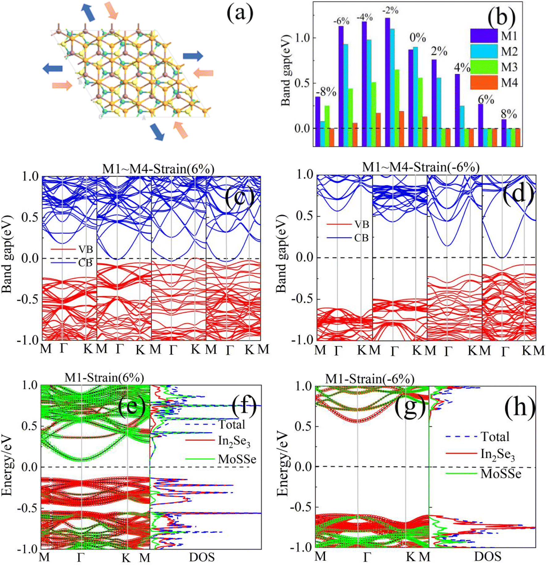 | ||
| Fig. 6 (a) Schematic diagram of the In2Se3/MoSSe heterostructure under biaxial strain and (b) the Eg as a function of the horizontal biaxial strain. (c) and (d) Band structures of M1–M4 with −6% and 6% strain, (e) and (g) the band structures, (f) and (h) the projected density of states (PDOS) under 6%, and −6% strain for M1. | ||
Fig. 6(e)–(h) show the band structures and PDOS of M1 under 6% and −6% strain, in which we can see that the band alignment of M1 demonstrated the type-II nature with ε = 6%, and the states in the VBM comprised the In2Se3 monolayer, but the CBM originated from the MoSSe monolayer which was different from that for the equilibrium state shown in Fig. 3(a). Moreover, the CBM and VBM moved to the Fermi level, which resulted in a decrease in Eg. The conduction bands of MoSSe exhibited a down shift, while the valence bands of In2Se3 moved up compared with the equilibrium state. When applying −6% compressive strain, it is worth noting that the In2Se3/MoSSe heterostructure had an indirect Eg of 1.13 eV for both the CBM and VBM, showing the trend of moving away from the Ef, which was in the proper range of 1.0–1.5 eV for solar cell devices. The CBM and VBM originated from the two constituents of the heterostructure, indicating that the coupling between In2Se3 and MoSSe was relatively strong, as shown in Fig. 6(h). As a result, the horizontal strain can greatly affect the band alignment type, the band structure shape, and the transition between a semiconductor and metal for the In2Se3/MoSSe heterostructure because the strain can induce changes in the bonds between atoms, the interfacial distances and interactions, as well as the PC6/WS2 heterostructure.54
3.4 Electric field effects on In2Se3/MoSSe vdW heterostructures
In addition, the different charge densities on the two surfaces of the out-of-plane polarized ferroelectric material can lead to different near-neighbor effects produced by the material bound to it. In conclusion, 2D ferroelectric materials with out-of-plane polarization provide a new avenue for electric field regulation of the physical properties of stacked 2D vdW heterostructures. Tuning the external electric field (Eext) is an important way to regulate the electronic properties of these heterostructures, whereby Eext is related to the vertical interface of these In2Se3/MoSSe heterostructures, as shown in Fig. 7(a), where the positive direction of Eext was from the MoSSe to In2Se3 monolayer. The electronic structure of the In2Se3/MoSSe heterostructure can vary greatly, but the geometry does not change much under different Eext values.55 Fig. 7(b) shows the variation of Eg with Eext in the range of −0.6–0.6V Å−1 with steps of 0.1 V Å−1, where the Eg of M2 showed an obvious difference with other models under Eext, whereby when a positive Eext is applied to these models, the Eg of M1 (M3 and M4) decreased linearly, especially the Eg of M3, which was zero after Eext = 0.5 V Å−1. The Eg of M2 reached a maximum value of 1.05 eV with Eext = 0.1V Å−1, and then dropped continuously with an increasing positive Eext. The Eg of M2 decreased rapidly with the increasing Eext under negative Eext, whereby the Eg of M2 was zero after Eext = −0.4 V Å−1, and it undergoes a transition in electronic properties from a semiconductor to metal. Noticeably, when Eext < 0, the Eg of M1 (M3 and M4) first linearly increased with Eext, reaching a maximum value of 0.90 (1.03, 1.19) eV at Eext = −0.1 (−0.2, −0.5) V Å−1. Then, it decreased gradually with increasing Eext. Fig. 7(c) shows the variation of band structures in detail for M2 with Eext = ±0.2, ±0.4, and ±0.6 V Å−1, respectively. It is clear that the band edge positions changed significantly under positive and negative Eext, which fully reflected an obvious electric field effect. The DOS and PDOS of M2 at Eext = ±0.2, ±0.4, and ±0.6 V Å−1 are given in Fig. 7(d)–(f). For M2, it was found to belong to a type-I heterostructure at the equilibrium state, as shown in Fig. 3(c). The electric field effects led to differences in the local electrostatic potential energy (LEPE) between the MoSSe and In2Se3 monolayers. When a positive Eext acted on M2, the LEPE on the MoSSe monolayer was larger than that on the In2Se3 monolayer, and the energy band of MoSSe (In2Se3) moved monotonically upward (downward) as Eext increased. We can see that the CBM states were consistently provided by In2Se3, but the VBM states originated by MoSSe with the applied positive Eext = 0.2, 0.4, and ±0.6 V Å−1. This means M2 was a type-II heterostructure when Eext exceeded 0.2 V Å−1. The value of the Eg of M2 depended on the CBM of In2Se3 and the VBM of MoSSe, whereby the CBM of In2Se3 decreased while the VBM state of MoSSe increased with the enhancement of Eext, thus the value of the Eg gradually decreased. The Eg of M2 reached a maximum when the CBM states of MoSSe and In2Se3 crossed at ∼0.1 V Å−1. When the electric field direction becomes a negative value, the energy band of MoSSe (In2Se3) will move downward (upward), and the VBM will be provided by In2Se3, but the CBM states originate from MoSSe, and thus, M2 will change from a type-I to type-II heterostructure when applying a negative Eext. Also, the Eg will decrease further with the CBM and VBM approaching the Ef gradually; especially, when the negative Eext is over 0.4 V Å−1, the Eg will be zero for the VBM of In2Se3 to reach or pass through the Ef. According to the above analysis process, we can also explain the various Eg values on the Eext for other models. A type-II band alignment at the equilibrium state with a small Eg was observed for M4, as shown in Fig. 3(g). When a positive Eext was applied, the CBM of In2Se3 and the VBM of MoSSe shifted toward the Ef because of the electric field effect, resulting in the Eg diminishing rapidly at a small Eext. On the contrary, the CBM of In2Se3 and the VBM of MoSSe moved far away the Ef, leading to an increasing Eg under the negative Eext, as shown in Fig. 7(g). For M3, the natures of the band structures were like as for M4, and the Eg showed a similar altering trend under the Eext. The maximum values of Eg (0.9, 1.05, 1.03, and 1.09 eV) were obtained under different Eext (−0.1, 0.1, −0.2, and 0.5 eV Å−1) because of the different moving speeds of the band edges for M1–M4. Ultimately, we briefly discuss the possibility based on the M4 heterostructure acting as a ferroelectric diode. The proposed device geometry is shown in Fig. 7(h), with the electrodes made of graphene molecular layers or metals located at each end of the heterostructured system. As can be noted from what was discussed above, Eext can tune the Eg of heterogeneous structures, especially in small negative biases, where the Eg of heterogeneous structures increased dramatically in a linear form. Therefore, the transmitting current between two electrodes was very small. However, when a small positive bias was applied, the electrons could easily transit and a larger current could be obtained, showing a rectifying effect.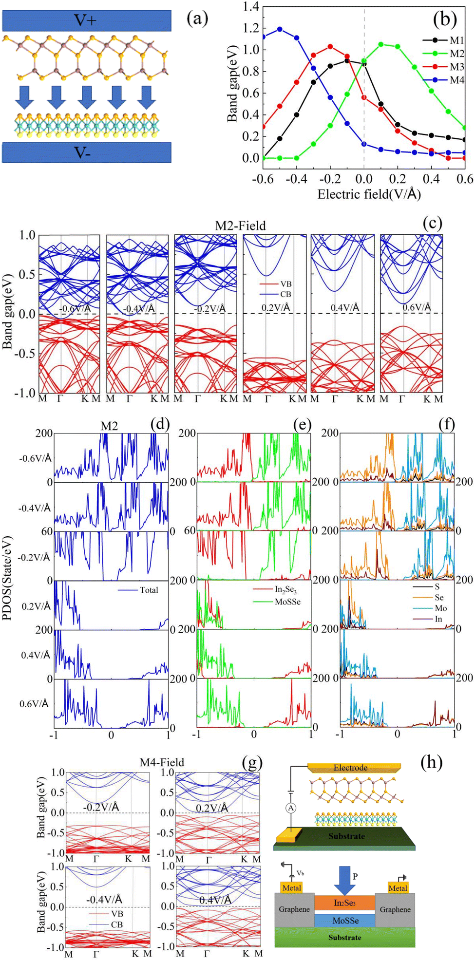 | ||
| Fig. 7 (a) Schematic illustration of the synergistic effects of the external perpendicular electric field, and the positive direction of the Eext from In2Se3 to MoSSe, (b) Eg as a function of the Eext for M1–M4, (c) and (g) the band structure of M2 and M4 with selected Eext, (d)–(f) PDOS of M2 under the selected Eext of ±0.2, ±0.4, and ±0.6V Å−1. (h) Ferroelectric diode (up) and mechanical switch device (down) based on M4. | ||
4 Conclusion
In summary, the electronic properties of four In2Se3/MoSSe heterostructures were studied using density functional theory based on first-principles calculations. These results showed that these heterostructures had type-I, type-II, and other band arrangements in the intrinsic state. The four In2Se3/MoSSe heterostructures exhibited obvious Eg differences ranging from 0.13 to 0.90 eV by PBE (0.47 to 1.50 eV by HSE06). The energy band could be regulated effectively by the vertical (horizontal) strain, and vertical interface electric field, and then the transformation from a semiconductor to metal could be obtained. The vertical strains (ε) more obviously affected the electronic properties for M1 and M4 than for the other models. The Eg values of M1–M4 showed a decreasing trend under the biaxial stretch strain, while they increased monotonously at first, reached the maximum value at ε = 2%, and then gradually lessened with the compressive strain. The Eg variation trend of M2 was opposite to that of the other models (M1, M3, and M4) when an electric field was applied. We designed a mechanical switching device and a ferroelectric diode based on the calculated data and applied vertical strain to the model and an external electric field effect. These results demonstrated the vdW heterostructures based on reversible spontaneous electric polarization materials have more flexible regulating avenues, which could be expected to aid the design of new functional devices.Author contribution
Y. Zhang: investigation, formal analysis, writing the original draft. X. Q. Deng: investigation, formal analysis, conceptualization. Q. Jing: methodology, formal analysis. Z. H. Zhang: resources, supervision, project administration. X. Ding: methodology, formal analysis.Conflicts of interest
The authors declare that they have no known competing financial interests or personal relationships that could have appeared to influence the work reported in this paper.Acknowledgements
This work was supported by Hunan Provincial Natural Science Foundation of China (Grant No. 2021JJ30733), and Hunan Provincial Innovation Foundation for Postgraduate (Grant No. CX20210828), and the Open Research Fund of Hunan Provincial Key Laboratory of Flexible Electronic Materials Genome Engineering (Grant No. 202008 and 202013).References
- K. S. Novoselov, A. K. Geim and S. V. Morozov, et al., Electric field effect in atomically thin carbon films, Science, 2004, 306(5696), 666–669 CrossRef CAS PubMed.
- K. S. Novoselov and A. K. Geim, The rise of graphene, Nat. Mater., 2007, 6(3), 183–191 CrossRef PubMed.
- P. Wang, S. Orimo and T. Matsushima, et al., Hydrogen in mechanically prepared nanostructured h-BN: a critical comparison with that in nanostructured graphite, Appl. Phys. Lett., 2002, 80(2), 318–320 CrossRef CAS.
- J. Liu, T. Zhang and Z. Wang, et al., Simple pyrolysis of urea into graphitic carbon nitride with recyclable adsorption and photocatalytic activity, J. Mater. Chem., 2011, 21(38), 14398–14401 RSC.
- S. Cao, J. Low, J. Yu and M. Jaroniec, Polymeric photocatalysts based on graphitic carbon nitride, Adv. Mater., 2015, 27(13), 2150–2176 CrossRef CAS PubMed.
- T. F. Jaramillo, K. P. Jørgensen and J. Bonde, et al., Identification of active edge sites for electrochemical H2 evolution from MoS2 nanocatalysts, Science, 2007, 317(5834), 100–102 CrossRef CAS PubMed.
- B. Radisavljevic, A. Radenovic and J. Brivio, et al., Single-layer MoS2 transistors, Nat. Nanotechnol., 2011, 6(3), 147–150 CrossRef CAS PubMed.
- O. Lopez-Sanchez, D. Lembke and M. Kayci, et al., Ultrasensitive photodetectors based on monolayer MoS2, Nat. Nanotechnol., 2013, 8(7), 497–501 CrossRef CAS PubMed.
- P. Zhao, Y. Ma and X. Lv, et al., Two-dimensional III2-VI3 materials: promising photocatalysts for overall water splitting under infrared light spectrum, Nano Energy, 2018, 51, 533–538 CrossRef CAS.
- L. Wang, Y. Zhang and L. Chen, et al., 2D polymers as emerging materials for photocatalytic overall water splitting, Adv. Mater., 2018, 30(48), 1801955 CrossRef PubMed.
- K. Zheng, H. Cui and H. Luo, et al., Two-dimensional penta-SiAs2: a potential metal-free photocatalyst for overall water splitting, J. Mater. Chem. C, 2020, 8(34), 11980–11987 RSC.
- F. Li, W. Wei and P. Zhao, et al., Electronic and optical properties of pristine and vertical and lateral heterostructures of Janus MoSSe and WSSe, J. Phys. Chem. Lett., 2017, 8(23), 5959–5965 CrossRef CAS PubMed.
- R. Peng, Y. Ma and S. Zhang, et al., Valley polarization in Janus single-layer MoSSe via magnetic doping, J. Phys. Chem. Lett., 2018, 9(13), 3612–3617 CrossRef CAS PubMed.
- S. D. Guo, Phonon transport in Janus monolayer MoSSe: a first-principles study, Phys. Chem. Chem. Phys., 2018, 20(10), 7236–7242 RSC.
- S. Deng, L. Li and O. J. Guy, et al., Enhanced thermoelectric performance of monolayer MoSSe, bilayer MoSSe and graphene/MoSSe heterogeneous nanoribbons, Phys. Chem. Chem. Phys., 2019, 21(33), 18161–18169 RSC.
- A. Y. Lu, H. Zhu and J. Xiao, et al., Janus monolayers of transition metal dichalcogenides, Nat. Nanotechnol., 2017, 12(8), 744–749 CrossRef CAS PubMed.
- J. Zhang, S. Jia and I. Kholmanov, et al., Janus monolayer transition-metal dichalcogenides, ACS Nano, 2017, 11(8), 8192–8198 CrossRef CAS PubMed.
- Z. Guan, S. Ni and S. Hu, Tunable electronic and optical properties of monolayer and multilayer Janus MoSSe as a photocatalyst for solar water splitting: a first-principles study, J. Phys. Chem. C, 2018, 122(11), 6209–6216 CrossRef CAS.
- X. Ma, X. Yong and C. Jian, et al., Transition metal-functionalized Janus MoSSe monolayer: a magnetic and efficient single-atom photocatalyst for water-splitting applications, J. Phys. Chem. C, 2019, 123(30), 18347–18354 CrossRef CAS.
- J. Qiao, F. Song and J. Hu, et al., Ultrathin MoSSe alloy nanosheets anchored on carbon nanotubes as advanced catalysts for hydrogen evolution, Int. J. Hydrogen Energy, 2019, 44(31), 16110–16119 CrossRef CAS.
- M. A. Lukowski, A. S. Daniel and F. Meng, et al., Enhanced hydrogen evolution catalysis from chemically exfoliated metallic MoS2 nanosheets, J. Am. Chem. Soc., 2013, 135(28), 10274–10277 CrossRef CAS PubMed.
- C. F. Fu, J. Sun and Q. Luo, et al., Intrinsic electric fields in two-dimensional materials boost the solar-to-hydrogen efficiency for photocatalytic water splitting, Nano Lett., 2018, 18(10), 6312–6317 CrossRef CAS PubMed.
- C. Cui, W. J. Hu and X. Yan, et al., Intercorrelated in-plane and out-of-plane ferroelectricity in ultrathin two-dimensional layered semiconductor In2Se3, Nano Lett., 2018, 18(2), 1253–1258 CrossRef CAS PubMed.
- S. Zhang, D. Xu and X. Chen, et al., Construction of ultrathin 2D/2D g-C3N4/In2Se3 heterojunctions with high-speed charge transfer nanochannels for promoting photocatalytic hydrogen production, Appl. Surf. Sci., 2020, 528, 146858 CrossRef CAS.
- Y. Liu, Y. Huang and X. Duan, Van der Waals integration before and beyond two-dimensional materials, Nature, 2019, 567(7748), 323–333 CrossRef CAS PubMed.
- K. Tran, G. Moody and F. Wu, et al., Evidence for moiré excitons in van der Waals heterostructures, Nature, 2019, 567(7746), 71–75 CrossRef CAS PubMed.
- J. Li, X. Yang and Y. Liu, et al., General synthesis of two-dimensional van der Waals heterostructure arrays, Nature, 2020, 579(7799), 368–374 CrossRef CAS PubMed.
- S. J. Liang, B. Cheng and X. Cui, et al., Van der Waals heterostructures for high-performance device applications: challenges and opportunities, Adv. Mater., 2020, 32(27), 1903800 CAS.
- W. Liao, Y. Huang and H. Wang, et al., Van der Waals heterostructures for optoelectronics: progress and prospects, Appl. Mater. Today, 2019, 16, 435–455 CrossRef.
- G. Wang, C. Chen and B. S. Teketel, et al., Constructing a new 2D Janus black phosphorus/SMoSe heterostructure for spontaneous wide-spectral-responsive photocatalytic overall water splitting, Int. J. Hydrogen Energy, 2021, 46(79), 39183–39194 CrossRef CAS.
- P. Lou and J. Y. Lee, GeC/GaN vdW heterojunctions: a promising photocatalyst for overall water splitting and solar energy conversion, ACS Appl. Mater. Interfaces, 2020, 12(12), 14289–14297 CrossRef CAS PubMed.
- C. V. Nguyen, V. T. T. Vi and L. T. T. Phuong, et al., Electronic structure and band alignment of Blue Phosphorene/Janus ZrSSe heterostructure: a first principles study, Phys. E, 2020, 124, 114369 CrossRef CAS.
- https://www.fermitech.com.cn/wiki/doku.php?id=start.
- X. Q. Deng, R. Q. Sheng and Q. Jing, Tunable electronic and optical properties of a BAs/As heterostructure by vertical strain and external electric field, RSC Adv., 2021, 11(35), 21824–21831 RSC.
- Z. Q. Fan, Z. H. Zhang and S. Y. Yang, High-performance 5.1 nm in-plane Janus WSeTe Schottky barrier field effect transistors, Nanoscale, 2020, 12(42), 21750–21756 RSC.
- W. A. Al-Saidi, V. K. Voora and K. D. Jordan, An assessment of the vdW-TS method for extended systems, J. Chem. Theory Comput., 2012, 8(4), 1503–1513 CrossRef CAS PubMed.
- W. A. Saidi, Van der Waals epitaxial growth of transition metal dichalcogenides on pristine and N-doped graphene, Cryst. Growth Des., 2014, 14(10), 4920–4928 CrossRef CAS.
- S. Grimme, Accurate description of van der Waals complexes by density functional theory including empirical corrections, J. Comput. Chem., 2004, 25(12), 1463–1473 CrossRef CAS PubMed.
- S. Deng, L. Li and P. Rees, Graphene/MoXY heterostructures adjusted by interlayer distance, external electric field, and strain for tunable devices, ACS Appl. Nano Mater., 2019, 2(6), 3977–3988 CrossRef CAS.
- H. U. Din, M. Idrees and T. A. Alrebdi, et al., Electric field tunable electronic properties of P–ZnO and SiC–ZnO van der Waals heterostructures, Comput. Mater. Sci., 2019, 164, 166–170 CrossRef CAS.
- Y. Shi, B. Song and R. Shahbazian-Yassar, et al., Experimentally validated structures of supported metal nanoclusters on MoS2, J. Phys. Chem. Lett., 2018, 9(11), 2972–2978 CrossRef CAS PubMed.
- W. A. Saidi, Van der Waals epitaxial growth of transition metal dichalcogenides on pristine and N-doped graphene, Cryst. Growth Des., 2014, 14(10), 4920–4928 CrossRef CAS.
- H. Hu and G. Ouyang, First-principles calculations of interface engineering for 2D α-In2Se3-based van der Waals multiferroic heterojunctions, Appl. Surf. Sci., 2021, 545, 149024 CrossRef CAS.
- T. N. Do, C. V. Nguyen and M. Idrees, et al., Strain engineering of the electro-optical and photocatalytic properties of single-layered Janus MoSSe: first principles calculations, Optik, 2020, 224, 165503 CrossRef CAS.
- C. Palacios-Berraquero, Atomically-thin quantum light emitting diodes, Quantum confined excitons in 2-dimensional materials, Springer, Cham, 2018, pp. 71–89 Search PubMed.
- R. S. Levitskii, A. V. Ivanov and E. Y. Perlin, The photon-avalanche effect in type-I heterostructures with deep quantum wells, J. Opt. Technol., 2006, 73(2), 71–75 CrossRef.
- X. Q. Deng and Q. Jing, Tunable electronic and optical properties of InSe/arsenene heterostructure by vertical strain and electric field, Phys. Lett. A, 2021, 405, 127427 CrossRef CAS.
- Z. Guan, C. S. Lian and S. Hu, et al., Tunable structural, electronic, and optical properties of layered two-dimensional C2N and MoS2 van der Waals heterostructure as photovoltaic material, J. Phys. Chem. C, 2017, 121(6), 3654–3660 CrossRef CAS.
- M. M. Furchi, F. Höller and L. Dobusch, et al., Device physics of van der Waals heterojunction solar cells, npj 2D Mater. Appl., 2018, 2(1), 1–7 CrossRef.
- D. Chen, X. Lei and Y. Wang, et al., Tunable electronic structures in BP/MoSSe van der Waals heterostructures by external electric field and strain, Appl. Surf. Sci., 2019, 497, 143809 CrossRef CAS.
- Y. Zhou, D. Wu and Y. Zhu, et al., Out-of-plane piezoelectricity and ferroelectricity in layered α-In2Se3 nanoflakes, Nano Lett., 2017, 17(9), 5508–5513 CrossRef CAS PubMed.
- X. He, X. Q. Deng and L. Sun, et al., Electronic and optical properties and device applications for antimonene/WS2 van der Waals heterostructure, Appl. Surf. Sci., 2022, 578, 151844 CrossRef CAS.
- P. Du, Y. Huang and J. Wang, et al., The electronic and optical properties of PC6/WS2 heterostructure modulated via biaxial strain and external electric field, Surf. Interfaces, 2021, 24, 101100 CrossRef CAS.
- W. Xiong, C. Xia and J. Du, et al., Band engineering of the MoS2/stanene heterostructure: strain and electrostatic gating, Nanotechnology, 2017, 28(19), 195702 CrossRef PubMed.
- Y. H. Xu, Z. Q. Fan and Z. H. Zhang, et al., Electronic and transport properties of GaAs/InSe van der Waals heterostructure, Appl. Surf. Sci., 2021, 547, 149174 CrossRef CAS.
| This journal is © The Royal Society of Chemistry 2023 |