
 Open Access Article
 This Open Access Article is licensed under a Creative Commons Attribution-Non Commercial 3.0 Unported Licence
Effect of heterojunction structures on photoelectrochemical properties of ZnTe-based photocathodes for water reduction
Tooru Tanaka *a,
Ryusuke Tsutsumia,
Tomohiro Yoshinagaa,
Takaki Sonoyamaa,
Katsuhiko Saitoa,
Qixin Guoa and
Shigeru Ikedab
*a,
Ryusuke Tsutsumia,
Tomohiro Yoshinagaa,
Takaki Sonoyamaa,
Katsuhiko Saitoa,
Qixin Guoa and
Shigeru Ikedab
aDepartment of Electrical and Electronic Engineering, Saga University, Saga 840-8502, Japan. E-mail: ttanaka@cc.saga-u.ac.jp
bDepartment of Chemistry, Konan University, Kobe, Hyogo 658-8501, Japan
First published on 22nd December 2022
Abstract
Photoelectrochemical (PEC) properties of ZnTe-based photocathodes with various structures were investigated to clarify the effective structure for the water reduction reaction. Samples with n-ZnO/ZnTe/p-ZnTe and n-ZnS/ZnTe/p-ZnTe heterostructures showed superior PCE properties to the samples without a heterojunction. In particular, the n-ZnS/ZnTe/p-ZnTe sample exhibited a large photocurrent even at a low applied potential in an electrolyte containing Eu3+ ion as an electron scavenger. Appreciable H2 evolution with a constant rate (approximately 87 μmol cm−2 h−1) was also observed over the sample loaded with Pt deposits under visible-light irradiation (>420 nm): faradaic efficiency of almost 100% was obtained, indicating no unfavorable side reaction occurred in the sample.
1. Introduction
Solar energy, the trump card of renewable energy, is inexhaustible, clean, and abundant. The amount of solar energy reaching the earth is estimated to be about 8000 times the world's total energy demand, which is so large that it is possible to obtain in one hour the energy required by mankind in one year.Photovoltaic power generation, which directly converts the energy of sunlight into electricity, is currently being introduced and utilized around the world. However, the grid stability issues have often become apparent due to its mass introduction, and it is important to develop new technologies from the viewpoint of energy storage. Artificial photosynthesis is therefore attracting attention as a technology for converting solar energy into clean hydrogen that can be stored.
There are several technologies to produce hydrogen from sunlight: (1) water splitting using electricity generated by solar cells,1 (2) simultaneous evolution of hydrogen and oxygen using photocatalysts,2 and (3) the use of two photoelectrodes for hydrogen and oxygen generation.3–8
At present, the highest solar-to-hydrogen (STH) efficiency of 24.4% (ref. 1) has been reported by combining concentrator photovoltaic modules and electrochemical cells with respect to the technology (1). The methods (2) requires only one type of photocatalysts, and can generate hydrogen with a simple structure. A very high quantum efficiency of almost unity has been reported using a modified aluminium-doped strontium titanate (SrTiO3![[thin space (1/6-em)]](https://www.rsc.org/images/entities/char_2009.gif) :Al) photocatalyst.2
:Al) photocatalyst.2
As for the hydrogen evolution technologies using photoelectrode (3), several semiconductor materials including CuIn0.5Ga0.5Se2,3 Cu2ZnSnS4 (CZTS),4,5 Cu2O,6 and CuGaSe2 (CGSe),7,8 have been investigated, and the highest half-cell solar-to-hydrogen (HC-STH) efficiency of 8% was obtained with a Rb-doped CGSe photocathode.8 This efficiency is relatively high but further improvement is still required for the practical applications.
To be used as hydrogen-evolving photoelectrodes, the energy of the conduction band minima must be higher than the reduction potential of H+ into H2, and the band gap energy should be as small as possible for efficient absorption of sunlight. It is also important to efficiently collect carriers generated by photon absorption in the semiconductor. Therefore, a pn junction is often formed,7,8 that can enhance the carrier collection by an internal electric field, using a material with no significant energy difference at the bottom of the conduction band (very small conduction offset).
II–VI semiconductor ZnTe is a promising material for a variety of optoelectronic device applications such as light-emitting diodes (LEDs)9,10 and solar cells11 because of its direct transition band gap energy of 2.26 eV at room temperature. So far, a pure green LED with the emission wavelength at 555 nm at room temperature has been developed using ZnTe.9 This material can absorb visible ray up to 550 nm and the conduction band locates higher energy than the reduction potential of H+ into H2. Therefore it is expected to use for photocathode application to produce hydrogen by water reduction reaction.
In ZnTe, because n-type doping is not easy due to so-called self-compensation effect,12 heterojunction structure is often used to realize pn-junction based optoelectronic devices.13,14 So far, CdS/ZnTe or ZnO/ZnTe heterojunction structures have been investigated for photochemical reduction of water15 or CO2.16,17 In ref. 15, the Pt/CdS/ZnTe heterojunction structures were used as a photocathode for hydrogen evolution from water and the enhanced photocurrent was reported by incorporation of Cu into ZnTe and surface modification with Mo and Ti layers. In order to improve photoreduction properties using ZnTe, it is important to clarify the correlation between the photocathode structure and photoelectrochemical (PEC) properties under light illumination.
Since the electron affinity of CdS is reported as 4.5–4.96 eV,18,19 a large conduction band offset (CBO) is expected at the heterointerface between CdS and ZnTe with an electron affinity of 3.5 eV.20,21 On the other hands, electron affinities of ZnO and ZnS are reported as 4.3–4.6 eV (ref. 22–26) and 3.9 eV,20 respectively, and thus, the smaller CBOs are expected. Especially, the internal electric field near the hetero interface is expected to be higher in ZnS/ZnTe structure as compared to other structures, that could result in higher collection efficiency of photoexcited carriers. In fact, we have already confirmed the higher open circuit voltage in ZnS/ZnTe solar cells.14,27
Here, we compare the photoelectrochemical properties of the ZnTe-based electrodes that consist of ZnTe/p-ZnTe substrate, n-ZnO/ZnTe/p-ZnTe, and n-ZnS/ZnTe/p-ZnTe heterostructures to clarify the effect of heterojunction structure on PEC properties of ZnTe-based photocathodes for water reduction reaction.
2. Experimental
Samples with structures of undoped ZnTe (thickness t = 300 nm)/p-ZnTe(100) substrate (#1), n-ZnO (t = 50 nm)/undoped ZnTe (t = 300 nm)/p-ZnTe(100) substrate (#2), n-ZnS (t = 50 nm)/undoped ZnTe (t = 300 nm)/p-ZnTe(100) substrate (#3) were prepared by molecular beam epitaxy (MBE) with a radio frequency (RF) radical cell for oxygen. The background pressure of the growth chamber before the growth is less than 6 × 10⁻⁸ Pa. 7N Zn, 6N Te, and 6N ZnS compound purchased from Asahi Metal Co., Ltd were used as source materials for the growth, and the 6N Al purchased from OS TECH Co., Ltd was used as a donor impurity source material in both n-ZnO and n-ZnS. p-ZnTe(100) substrates purchased from JX Nippon Mining & Metals Corporation with the thickness of 500 μm were ultrasonically cleaned in organic solvents prior to wet-etching using a Br–methanol solution.In sample #1, an undoped ZnTe layer with the thickness of 300 nm was grown by MBE at 400 °C on the p-ZnTe(100) substrate.
In sample #2, after the growth of an undoped ZnTe layer with the thickness of 300 nm at 400 °C on the p-ZnTe(100) substrate similar to #1, an Al-doped n-type ZnO layer with the thickness of 50 nm was grown by MBE at 250 °C. For n-ZnO growth, Zn, O, and Al were supplied on the surface of the film, where O was supplied as O radicals by using the RF radical cell with a RF power and an O2 flow rate of 300 W and 1 sccm, respectively.
In sample #3, after the growth of an undoped ZnTe layer with the thickness of 300 nm at 400 °C on the p-ZnTe(100) substrate similar to #1, an Al-doped n-type ZnS layer with the thickness of 50 nm was grown by MBE at 250 °C. For n-ZnS growth, ZnS and Al were supplied on the surface of the film. To characterize the surface crystallinity, a reflection high-energy electron diffraction (RHEED) was monitored during the MBE growth. After the MBE growth, Pd ohmic contact was deposited on the backside of all p-ZnTe substrates by electroless plating.
PEC properties were measured using a conventional three-electrodes setup. Three electrodes, namely, ZnTe-based electrode, Ag/AgCl, and Pt wire, as working, reference, and counter electrodes, respectively, were set into a three-necked flask with a flat window containing 0.2 M Eu(NO3)3 solution (pH 4). Since the Eu3+ ion works as an efficient electron acceptor for the p-type photocathode,28,29 the ZnTe-based electrode without any surface modifications was used. The surface area of the ZnTe-based electrode is approximately 5 mm × 5 mm. The potential sweep was controlled by a Hokuto Denko HSV-110 automatic polarization system. Measurements were conducted by a linear sweep voltametric (LSV) mode with a negative scan direction at the scan rate of 10 mV s−1 under chopped illumination of focused simulated sunlight (AM 1.5 G × 5 sun).
In order to examine water reduction (H2 production) properties of the ZnTe-based electrode, surface modification by deposition of Pt particles was performed. The electrolyte used for the Pt deposition was composed of 0.1 M Na2SO4 and 1 mM H2PtCl6 at pH adjusted to 4 using a diluted HCl solution; photoirradiation was performed by using a Cermax LX-300F 300 W xenon lamp at a fixed potential of −0.265 V (vs. RHE) for 30 s. An LSV plot for the water reduction over the ZnTe-based electrode under chopped illumination of the above 300 W xenon lamp with a long pass filter that can pass photons with the wavelength longer than 420 nm was recorded at pH 6.5 using a phosphate buffer solution (0.4 M K2HPO4/KH2PO4/K2SO4) as an electrolyte. This pH is close to the one usually used for the characterization for CZTS4,5 or CGSe7,8 photocathode, and the similar pH has been used in this study. The effect of the pH on the water reduction characteristics of ZnTe-based photocathodes will be the future work. Potentials for the PEC water reduction that referred to the Ag/AgCl electrode (VAg/AgCl) were converted to those that referred to the reversible hydrogen electrode (VRHE) by using the following equation:
| VRHE = VAg/AgCl + 0.059 × pH + 0.199. |
A PEC cell connected to an online gas chromatography system (Agilent 490 Micro GC Gas Analyzer equipped with an MS-5A column and a thermal conductivity detector) was used to obtain a time course curve of H2 liberation. The PEC cell was immersed in a water bath to maintain the temperature at 293 K, and photoirradiation was performed at 0 VRHE under the light illumination. The H2 evolution rate of the gas chromatography was calibrated prior to the H2 evolution measurements of the samples. The standard deviation during calibration is less than 1–2 μmol h−1.
3. Results and discussion
Fig. 1 shows the RHEED patterns after the growth of (a) undoped ZnTe of sample #1, (b) undoped ZnTe and (c) n-ZnO of sample #2, and (d) undoped ZnTe and (e) n-ZnS of sample #3. In all samples, the undoped ZnTe layers were epitaxially grown on p-ZnTe(100) substrates. After the growth of n-ZnO on undoped ZnTe in sample #2, the RHEED pattern changed to the ring pattern, as shown in Fig. 1(c), indicating the growth of polycrystalline n-ZnO layer. This is because of the different crystal structure between ZnTe with zinc blende structure and ZnO with wurtzite structure. On the other hand, the spot pattern was obtained after the growth of n-ZnS with zinc blende structure, indicating the epitaxial growth of n-ZnS on ZnTe. This result is consistent with the previous report.14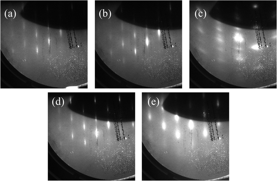 | ||
| Fig. 1 RHEED patterns after the growth of (a) undoped ZnTe of sample #1, (b) undoped ZnTe and (c) n-ZnO of sample #2, (d) undoped ZnTe and (e) n-ZnS of sample #3. | ||
Fig. 2 shows the scanning electron microscope image of the surface of sample #3. A very smooth surface of n-ZnS was observed. Similar smooth surfaces were observed for other samples. The inset of Fig. 2 shows the optical microscope image of the ZnTe-based photocathode.
 | ||
| Fig. 2 Scanning electron microscope image of the surface of sample #3. The inset shows the optical microscope image of the ZnTe-based photocathode. | ||
Typical electron concentration n, mobility μ, and resistivity ρ obtained for n-ZnO and n-ZnS grown on semi-insulating ZnTe(100) substrates under the same growth condition are nZnO = 1.4 × 1020 cm−3, μZnO = 0.6 cm2 V−1 s−1, and ρZnO = 7.4 × 10⁻² Ω cm, and nZnS = 3.3 × 1019 cm−3, μZnS = 28 cm2 V−1 s−1, and ρZnS = 6.7 × 10⁻³ Ω cm, respectively.
PEC current–voltage characteristics of ZnTe-based three electrodes were investigated by LSV measurement in an Eu3+ solution. Fig. 3 shows LSV plots of ZnTe-based electrodes with a ZnTe/p-ZnTe/Pd (#1), a n-ZnO/ZnTe/p-ZnTe/Pd (#2), and a n-ZnS/ZnTe/p-ZnTe/Pd (#3) structures in 0.1 M europium nitrate under chopped illumination of simulated sunlight (AM 1.5 G × 5 sun). In sample #1, although a photocurrent was small compared with other samples, the photocurrent increases with the increase of negative potential, indicating a PEC characteristic of p-type semiconductor. On the other hand, the samples #2 and #3 show significantly large photocurrents, and especially in #3, the photocurrent of 3.5 mA cm−2 was observed even at low potential of VRHE = 0 V.
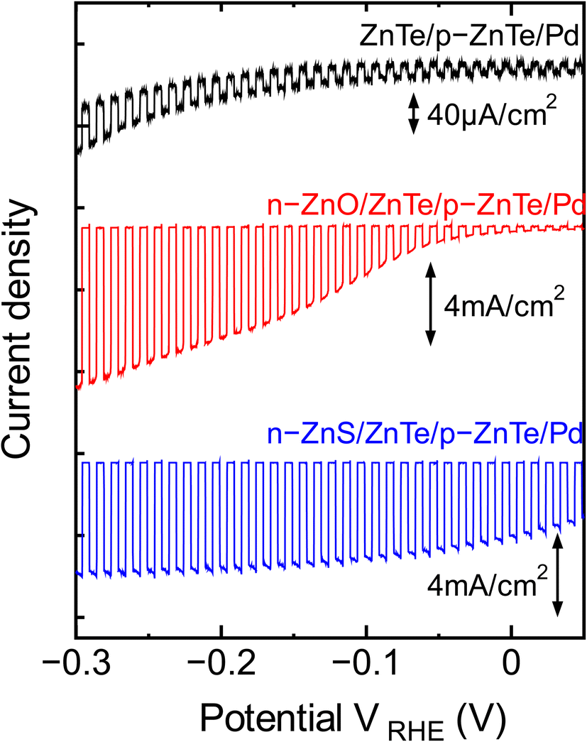 | ||
| Fig. 3 LSV plots of ZnTe-based electrodes with a ZnTe/p-ZnTe/Pd (#1), a n-ZnO/ZnTe/p-ZnTe/Pd (#2), and a n-ZnS/ZnTe/p-ZnTe/Pd (#3) structures in 0.1 M europium nitrate under chopped. | ||
Fig. 4 shows the electrode structure and energy band diagrams of ZnTe-based electrodes with a n-ZnO/ZnTe/p-ZnTe/Pd (#2) and a n-ZnS/ZnTe/p-ZnTe/Pd (#3) structures. The energy band diagrams were drawn using band gaps and electron affinities of 2.26 eV (ref. 30) and 3.53 eV (ref. 20 and 21) for ZnTe, 3.4 eV (ref. 31) and 4.5 eV (ref. 26) for ZnO, and 3.7 eV (ref. 32) and 3.9 eV (ref. 20) for ZnS. Because ZnS has a smaller electron affinity than ZnO, a higher internal electric field exists in the undoped ZnTe layer in sample #3, resulting in the higher collection efficiency of photoexcited electrons in ZnTe. This is the reason for higher photocurrent density in sample #3 even at low applied voltage. In sample #2, the photocurrent density increases with increasing negative potential, as shown in Fig. 3. This is attributed to the enhanced collection of photoexcited electrons by the increased negative applied potential.
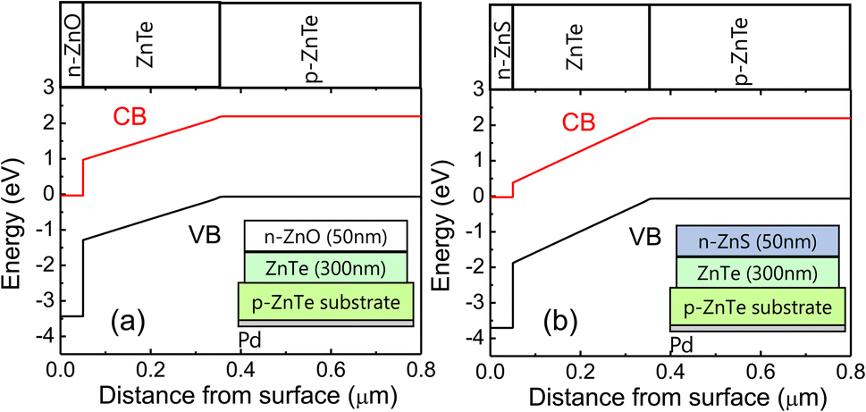 | ||
| Fig. 4 Electrode structure and energy band diagrams of ZnTe-based electrodes with (a) a n-ZnO/ZnTe/p-ZnTe/Pd (#2), and (b) a n-ZnS/ZnTe/p-ZnTe/Pd (#3) structures. | ||
To clarify the active area generating the photocurrent under light illumination, EQE spectra for sample #2 and #3 were measured and plotted in Fig. 5. The EQE for sample #3 is much larger than that for sample #2, consistent with photocurrent results. EQEs for both samples increase at the photon energy of approximately 2.2 eV corresponding to the band gap energy of ZnTe, and then, they decrease above 3.5 eV, which is almost consistent with the band gap energy of ZnO or ZnS. Therefore, the most photocurrent is found to be generated in ZnTe region.
 | ||
| Fig. 5 EQE spectra for sample #2 and #3. | ||
Fig. 6(a) shows an LSV plot in a pH 6.5 phosphate buffer solution obtained by a sample #3 electrode modified with Pt particle deposition (Pt–n-ZnS/ZnTe/p-ZnTe/Pd structure) under chopped illumination. A photocurrent increases gradually with increasing cathodic polarization. The primary event inducing the observed photocurrents is likely to be water reduction into H2.
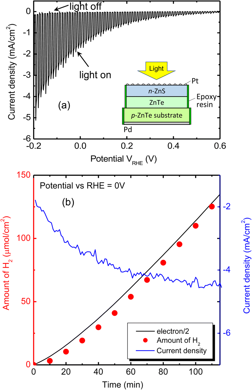 | ||
| Fig. 6 (a) LSV plot for a sample #3 electrode modified with Pt particle deposition (Pt–n-ZnS/ZnTe/p-ZnTe/Pd structure) under chopped illumination. (b) A time course curve of H2 liberation from a unit area of the electrode under illumination. | ||
In order to measure the amount of gas-phase H2 quantitatively, H2 liberation over the Pt–n-ZnS/ZnTe/p-ZnTe/Pd electrode at a fixed potential (VRHE = 0) was examined. Fig. 6(b) shows a time course curve of H2 liberation from a unit area of the electrode under illumination. A current density profile during light illumination is also plotted in this figure. The amount of H2 increases monotonically and then the rate becomes slightly larger, which is attributed to an increase of the photocurrent density over time. The rate of H2 liberation estimated from the slope of the plot at the latter half part (70–110 min) was approximately 87 μmol cm−2 h−1. Although the illuminated light intensity in this experiment is almost three times higher than the general simulated sunlight (AM1.5 G × 1 sun), we can see that relatively high H2 liberation rate was obtained using this structure. Faradaic efficiency, defined as the ratio in percent of the amount of H2 evolution to that of half electrons passing through the outer circuit (e−/2), was estimated to be almost 100%, as can be seen by comparing the amount of H2 with the e−/2 plotted in Fig. 6(b). This result indicates almost no unfavorable side reaction occurred in this sample. Therefore, the n-ZnS/ZnTe heterojunction structure is suitable for water reduction reaction.
Finally, we have examined a stability of ZnTe electrode with the sample #3 (Pt–n-ZnS/ZnTe/p-ZnTe/Pd) under illumination. The preliminary result of the stability test for 12 hours under AM1.5 G × 1 sun illumination is shown in Fig. 7. At the beginning, the photocurrent slightly increases up to 0.95 mA cm−2 but after 1 hour it gradually decreases with time and reaches to 0.81 mA cm−2 after 12 hours. The insets in Fig. 7 show the surface images of the sample before and after light irradiation. After the light irradiation, a part of the sample surface (bottom right) was seemed to be degraded by the photochemical reaction, and this degradation may be the reason for the decrease of photocurrent. In this sample, because the thickness of n-ZnS layer is only 50 nm, the partial degradation of ZnTe electrode by the solution might be occurred. Further improvement is expected by optimizing the structural parameters such as thicknesses or carrier concentration of n-ZnS and ZnTe layers and so on.
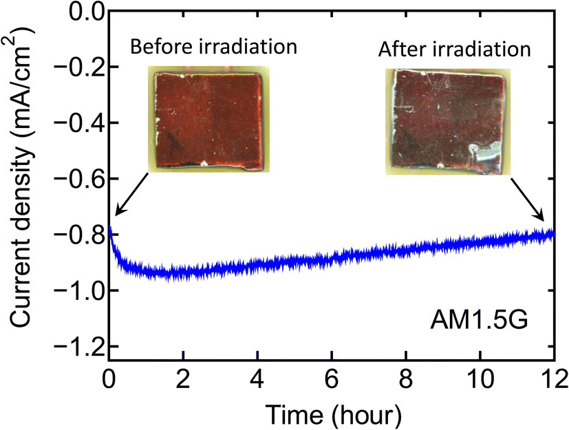 | ||
| Fig. 7 Preliminary result of stability test for 12 hours under AM1.5 G × 1 sun illumination for a sample #3 electrode modified with Pt particle deposition (Pt–n-ZnS/ZnTe/p-ZnTe/Pd structure). | ||
4. Conclusions
ZnTe-based photocathodes with heterostructures showed superior PEC properties for water reduction reaction as a result of improved carrier collection due to the existing internal electric field at pn-junction. Among the tested samples, n-ZnS/ZnTe/p-ZnTe structure exhibits the highest photocurrent even at low potential, and relatively high H2 liberation rate was obtained, indicating the possibility to use this structure for artificial solar water splitting.Conflicts of interest
There are no conflicts to declare.Acknowledgements
This work was partly supported by the JSPS KAKENHI Grant Numbers 18K19046, 19H02661, and 22K19000, and JKA and its promotion funds from KEIRIN RACE.References
- A. Nakamura, Y. Ota, K. Koike, Y. Hidaka, K. Nishioka, M. Sugiyama and K. Fujii, Appl. Phys. Express, 2015, 8, 107101 CrossRef.
- T. Takata, J. Jiang, Y. Sakata, M. Nakabayashi, N. Shibata, V. Nandal, K. Seki, T. Hisatomi and K. Domen, Nature, 2020, 581, 411 CrossRef CAS.
- H. Kobayashi, N. Sato, M. Orita, Y. Kuang, H. Kaneko, T. Minegishi, T. Yamada and K. Domen, Energy Environ. Sci., 2018, 11, 3003 RSC.
- D. Huang, K. Wang, L. Li, K. Feng, N. An, S. Ikeda, Y. Kuang, Y. Ng and F. Jiang, Energy Environ. Sci., 2021, 14, 1480 RSC.
- D. Huang, K. Wang, L. Yu, T. H. Nguyen, S. Ikeda and F. Jiang, ACS Energy Lett., 2018, 3, 1875 CrossRef CAS.
- A. Paracchino, V. Laporte, K. Sivula, M. Grätzel and E. Thimsen, Nat. Mater., 2011, 10, 456 CrossRef CAS.
- S. Ikeda, R. Okamoto and S. Ishizuka, Appl. Phys. Lett., 2021, 119, 083902 CrossRef CAS.
- S. Ishizuka, R. Okamoto and S. Ikeda, Adv. Mater. Interfaces, 2022, 9, 2201266 CrossRef CAS.
- T. Tanaka, Y. Kume, M. Nishio, Q. Guo, H. Ogawa and A. Yoshida, Jpn. J. Appl. Phys., 2003, 42, L362 CrossRef CAS.
- T. Tanaka, K. Saito, M. Nishio, Q. Guo and H. Ogawa, Appl. Phys. Express, 2009, 2, 122101 CrossRef.
- T. Tanaka, K. M. Yu, P. R. Stone, J. W. Beeman, O. D. Dubon, L. A. Reichertz, V. M. Kao, M. Nishio and W. Walukiewicz, J. Appl. Phys., 2010, 108, 024502 CrossRef.
- G. Mandel, Phys. Rev., 1964, 134, A1073 CrossRef.
- T. Tanaka, M. Miyabara, Y. Nagao, K. Saito, Q. Guo, M. Nishio, K. M. Yu and W. Walukiewicz, IEEE J. Photovoltaics, 2014, 4, 196 Search PubMed.
- T. Tanaka, K. M. Yu, Y. Okano, S. Tsutsumi, S. Haraguchi, K. Saito, Q. Guo, M. Nishio and W. Walukiewicz, IEEE J. Photovoltaics, 2017, 7, 1024 Search PubMed.
- T. Minegishi, A. Ohnishi, Y. Pihosh, K. Hatagami, T. Higashi, M. Katayama, K. Domen and M. Sugiyama, APL Mater., 2020, 8, 041101 CrossRef CAS.
- Y. J. Jang, J. Jang, J. Lee, J. H. Kim, H. Kumagai, J. Lee, T. Minegishi, J. Kubota, K. Domen and J. S. Lee, Energy Environ. Sci., 2015, 8, 3597 RSC.
- M. F. Ehsan, R. Khan and T. He, ChemPhysChem, 2017, 18, 3203 CrossRef CAS PubMed.
- A. G. Milnes and D. L. Feucht, Heterojunctions and Metal–Semiconductor Junctions, Academic, New York, 1972 Search PubMed.
- H. Sim, J. Lee, S. Cho, E. S. Cho and S. J. Kwon, J. Semicond. Technol. Sci., 2015, 15, 267 CrossRef.
- R. K. Swank, Phys. Rev., 1967, 153, 844 CrossRef CAS.
- H. Dumont, J. Bouree, A. Marbeuf and O. Gorochov, J. Cryst. Growth, 1993, 130, 600 CrossRef CAS.
- K. Ip, G. T. Thaler, H. S. Yang, S. Y. Han, Y. J. Li, D. P. Norton, S. J. Pearton, S. W. Jang and F. Ren, J. Cryst. Growth, 2006, 287, 149 CrossRef CAS.
- B. J. Coppa, R. F. Davis and R. J. Nemanich, Appl. Phys. Lett., 2003, 82, 400 CrossRef CAS.
- A. Kolmakov, D. O. Klenov, Y. Lilach, S. Stemmer and M. Moskovits, Nano Lett., 2005, 5, 667 CrossRef CAS PubMed.
- V. Dobrokhotov, D. N. McIlroy, M. G. Norton, A. Abuzir, W. J. Yeh, I. Stevenson, R. Pouy, J. Bochenek, M. Cartwright, L. Wang, J. Dawson, M. Beaux and C. Berven, J. Appl. Phys., 2006, 99, 104302 CrossRef.
- K. Jacobi, G. Zwicker and A. Gutmann, Work function, electron affinity and band bending of zinc oxide surfaces, Surf. Sci., 1984, 141, 109 CrossRef CAS.
- T. Tanaka, K. Matsuo, K. Saito, Q. Guo, T. Tayagaki, K. M. Yu and W. Walukiewicz, J. Appl. Phys., 2019, 125, 243109 CrossRef.
- J. J. Scragg, P. J. Dale and L. M. Peter, Electrochem. Commun., 2008, 10, 639 CrossRef CAS.
- S. Ikeda, T. Nakamura, S. M. Lee, T. Yagi, T. Harada, T. Minegishi and M. Matsumura, ChemSusChem, 2011, 4, 262 CAS.
- L. Bornstein, in Numerical Data and Functional Relationships in Science and Technology, ed. O. Madelung, H. Weiss and M. Schulz, Springer, Berlin, 1982 Search PubMed.
- H. Jang, K. Saito, Q. Guo, K. M. Yu and T. Tanaka, J. Phys. Chem. Solids, 2022, 163, 110571 CrossRef CAS.
- L. C. Olsen, R. C. Bohara and D. L. Barton, Appl. Phys. Lett., 1979, 34, 528 CrossRef CAS.
| This journal is © The Royal Society of Chemistry 2023 |