
 Open Access Article
 This Open Access Article is licensed under a Creative Commons Attribution-Non Commercial 3.0 Unported Licence
Engineered molecular stacking crystallinity of bar-coated TIPS-pentacene/polystyrene films for organic thin-film transistors†
Yongjin Jo‡
a,
Jonghan Lee‡ a,
Chaewon Kima,
Junhyeok Janga,
Inchan Hwangb,
John Hong*a and
Mi Jung Lee*a
a,
Chaewon Kima,
Junhyeok Janga,
Inchan Hwangb,
John Hong*a and
Mi Jung Lee*a
aSchool of Materials Science and Engineering, Kookmin University, Seoul, 02707, South Korea. E-mail: mijung@kookmin.ac.kr
bDepartment of Electronic Materials Engineering, Kwangwoon University, Seoul, 01897, South Korea
First published on 18th January 2023
Abstract
Solution-based blended polymer materials are promising for electronic applications in many fields. However, determining a controllable method to achieve electronically active organic films through the practical liquid deposition process is very challenging. In this study, we suggest employing hybrid binary organic mixture inks (an insulating polymer polystyrene (PS)) and an organic semiconductor (6,13-bis(triisopropylsilylethnyl)pentacene (TIPS-pentacene)) to manage and enhance the characteristics of TIPS-pentacene organic layers using a bar-coating method. Binary mixtures with PS molecules can provide various microstructures, crystal orientations, and molecular stacking of the active TIPS-pentacene organic layers under the proper fabrication parameters during bar-coating. Varying the molecular weight of the PS mixture, weight percentage of the TIPS-pentacene, and deposition parameters, such as the bar-coating speed, direction, and contact angles between the crystal orientation of TIPS-pentacene and Au electrodes, is crucial to guarantee high-electronic properties. The electrodes with TIPS-pentacene/PS (MW = 4000) binary films at a 40 wt% TIPS-pentacene ratio demonstrate the outstanding room-temperature field-effect mobility of 1.215 cm2 V−1 s−1, four times higher than that of pure TIPS-pentacene transistors (100 wt%). The performance improvement of the TIPS-pentacene layers is highly attributed to the ideal spherulite structure and thick molecular stacking properties, which can guarantee favorable charge transport paths through organic films. These findings demonstrate a promising strategy for blending organic applications to improve the performance of organic electronic devices using practical fabrication processes.
Introduction
The utilization of active and conductive electrode materials with high flexibility and stability is highly interesting for future electronic applications. Organic semiconductor materials have been considered promising candidates, owing to their cost-effective solution process and mechanical durability.1,2 Organic semiconductor/insulating polymer blended devices are possible to reduce process costs per unit cell compared to pristine organic semiconductor devices. The performance stability of polymer blended devices is higher than pristine organic devices according to the high mechanical properties of insulating polymers.3 Continued improvements in organic electronic devices primarily rely on the judicious control of the surface, morphology, and molecular stacking of organic thin films, directly correlating with the resulting electrical properties.However, strong molecular interaction originating from the π–π bonds of organic molecules usually causes nonuniform films, polymer aggregation, and distorted crystallinity, lowering the electrical mobility and performance of organic film-based devices. Therefore, overcoming these limitations is essential for their practical realization as future organic applications. In addition, determining a synthetic and controllable way to minimize the π–π bond interactions of organic materials is a major issue, which relies on better organic materials and deposition processes.
To date, blended binary organic semiconducting and insulating polymer mixtures have been promising as organic film candidates, whereas added insulating polymers can decrease the strong π–π bond interactions of semiconducting materials.3–5 In particular, the easy tunability of blending composites and their high compatibility with solution-based device fabrication processes make blended organic mixtures practicably suitable for tailoring the properties and scalability of organic devices.6,7
Insulating polymers could develop a favorable semiconductor–insulating polymer interface with proper structures and morphologies in organic field-effect transistors (FETs).8 Still, one of the main challenges in blending polymer fields is optimizing blended semiconducting and insulating organic mixture inks and the subsequent coating procedures. Among many different coating methods, such as solution-shearing,9–11 doctor-blading,12–14 and zone-casting,15–17 the bar-coating method has many practical traits for depositing target materials over large areas within a short time frame. However, the properties of blended organic mixture films with the bar-coating method in organic electronics have scarcely been reported.
In this paper, we report on the systematic studies of 6,13-bis(triisopropylsilylethynyl)pentacene (TIPS-pentacene) and polystyrene (PS) blended organic FETs fabricated using a facile bar-coating method. TIPS-pentacene is widely used p-type organic semiconductor material. It is promising material candidate for electronic applications due to its high stability, and resuability.4,18,19 The PS materials have been widely used in blended organic electronics due to their nonpolar functional groups, inducing the successful phase separation and structural development of TIPS-pentacene/PS blends.20 The morphology and electronic properties of TIPS-pentacene/PS blends have been examined to determine the optimized bar-coating procedures by changing the concentration and bar-coating speed of the organic solution and the molecular weight (MW) of PS polymers. Especially, as a first-proof of concept and application, after appropriate coating parameters, an optimum amount, speed and mixture of TIPS-pentacene/PS can induce two-dimensional (2D) spherulite morphology of TIPS-pentacene, which is crucial to improve the overall field-effect performance of FETs compared to other morphology of TIPS-pentacene.4
The morphology of the TIPS-pentacene layers was changed from needle-like one-dimensional (1D) structures to two-dimensional (2D) spherulite at the optimized fabrication parameters (especially at 40 wt% of TIPS-pentacene). The 2D spherulites of TIPS-pentacene layers can guarantee the high field-effect mobility of FETs compared to that of the needle-like 1D structures due to the high surface coverage of crystals with a unique continuous film structure. In addition, we demonstrated that the increased c-axis distance of TIPS-pentacene layers also provides more carrier paths along organic films. These findings suggest that a proper understanding of the mixture composites and bar-coating procedures is highly desirable to optimize the electrical properties of future blended organic-material electronics.
Experimental details
TIPS-pentacene/PS blended solution
The TIPS-pentacene, PS, trichloro(phenyl)silane (≥97.0%), and toluene (anhydrous, 99.8%) were purchased from Sigma Aldrich. The organic materials (TIPS-pentacene and PS) were dissolved in anhydrous toluene at concentrations from 2 to 16 mg mL−1. The entire ink process was conducted in a nitrogen glove box to prevent the degradation of materials by oxygen or moisture. The solution was kept on the stirrer at 60 °C for 30 min and was filtered using a 0.2 μm pore-sized PTFE filter. After filtering, both solutions were blended at different weight percentage (wt%) values.Device fabrication
A schematic illustration of the bar-coating deposition of blended organic films is presented in Fig. 1a. Generally, the size and quality of organic crystals can be tailored by the physical and chemical properties of the mixed solution, surface properties of the substrates (temperature and surface energy), and deposition parameters of the bar-coating.21 The pristine TIPS-pentacene or blended TIPS-pentacene/PS solution was dispersed on the bar-coating substrates. The bar-coating parameters can control the evaporation of the solution and, subsequently, manage the level of nucleation and crystal growth of the TIPS-pentacene films.22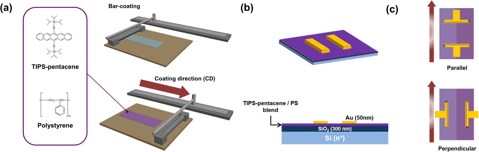 | ||
| Fig. 1 Schematic illustration of (a) bar-coating equipment and (b) TIPS-pentacene transistor. (c) Contact angle between TIPS-pentacene crystal and Au electrodes. | ||
Therefore, we systematically studied the device parameters of blended organic films while changing the film deposition conditions. The prepared solution was used to design the active organic layer using bar-coating. We used an n-type doped silicon substrate purchased from DASOM RMS with 3000 Å dry-oxidized SiO2 on top for device fabrication. After the cleaning steps, to generate the self-assembled monolayer surface on the substrate, trichloro(phenyl)silane in toluene was used for the surface treatment. The materials for self-assembled monolayer (SAM), such as octadecyltrichlorosilane (OTS) or trichloro(phenyl)silane (PTS), are generally treated on the surface of SiO2 substrate to reduce the trapping interface states of SiO2. Moreover, also the SAM treatment can change the affinity of SiO2, which can help the uniform deposition of the prepared solution.23,24 Finally, the substrate temperature was set to 40 °C during the coating procedures, and 100 μL of the blended organic solution was dropped onto the substrate. After the thin film formed, the substrate remained on the 50 °C hotplate for 5 min to remove the remaining solvent. A gold (Au) electrode was deposited using thermal evaporation to form the source/drain contact, as depicted in Fig. 1b. The contact angles of electrodes are defined by the measured angle between the direction of bar-coating (red arrow) and the Au electrode. Parallel and perpendicular angle devices were determined at a contact angle of 90° and 180°, respectively, as displayed in Fig. 1c.
Device characterization
The current–voltage curves were measured using an MS tech probe station with a Keithley 4200-SCS system. The X-ray diffraction (XRD) patterns were collected using a Rigaku Ultima IV diffractometer. The absorbance spectra of the TIPS-pentacene films were collected using a Cary 100 ultraviolet-visible (UV-vis) spectrometer (Agilent Technologies). The height profile and atomic force microscopy (AFM) images of the TIPS-pentacene film were acquired using an XE-100 microscope (Park Systems).Results and discussion
The electrical properties of the TIPS-pentacene-only films were characterized by varying the deposition conditions, such as the concentrations and coating speed. AFM images were used to investigate the surface morphology and height profile of the samples. Fig. S1 (ESI†) illustrates the surface morphology (crystal sizes and orientations) of the TIPS-pentacene-only films using an optical microscope and AFM. The crystals of the TIPS-pentacene-only films form only after a specific concentration (over 8 mg mL−1) due to the lack of nuclei formation at concentrations of 2 to 6 mg mL−1. At a concentration of 8 mg mL−1, the crystal growth of TIPS-pentacene starts, but the crystal orientation and grain width cannot be clearly defined. At concentrations over 10 mg mL−1, the crystal domains and orientations are detected, and the grain widths increase as the TIPS-pentacene concentration increases.Electrical characteristics
The electrical characteristics were measured by 3-terminal FET probe station to compare the electrical performance of the devices which are fabricated by the different coating process and parameters. Fig. S2 (ESI†) presents the current–voltage (I–V) curves of the TIPS-pentacene-only films with different concentrations. Two types of OFET devices exist according to the contact angles between the direction of bar-coating and the Au electrode (parallel and perpendicular configurations). The field-effect mobilities of TIPS-pentacene-only films can be extracted from the square root values of the transfer curve, and the extracted mobilities are illustrated in Fig. 2a.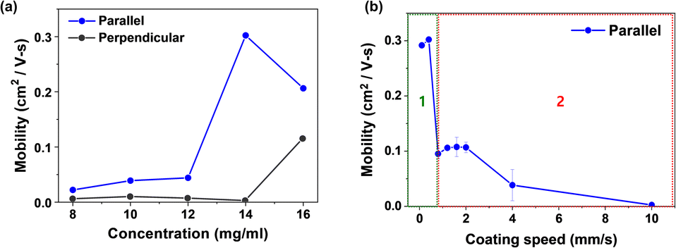 | ||
| Fig. 2 Saturation mobility of TIPS-pentacene-only films with different (a) solution concentrations and (b) bar-coating speeds. | ||
Devices with parallel angles exhibit higher mobility values than those with perpendicular angles. The different contact-angle arrangements can result in different coverages of TIPS-pentacene layers on organic FETs. At a concentration of 14 mg mL−1 with the parallel device configuration, the mobility has the highest value of 0.284 cm2 V−1 s−1. In addition, with the same concentration of 14 mg mL−1, coating speeds are modulated from 0.1 to 10 mm s−1 to examine the effects of the residual solvent on the crystallization and morphological evolution of TIPS-pentacene.
Bar-coating speed is an important factor, which can largely affect the nucleation and crystal growth of TIPS-pentacene by modulating the evaporation rate of solvents. The film morphology and electrical properties for different bar-coating speeds are presented in Fig. S3 and S4 (ESI†), respectively. When the bar-coating speed is low (0.1 to 0.4 mm s−1), the needle-like TIPS-pentacene films form, and the crystal orientation is parallel to the bar-coating direction. The low evaporation rate for the low coating speed can provide a relatively long growth time to arrange the nuclei formation through the bar-coating direction.
However, when the bar-coating speed is increased to 0.8 mm s−1, the crystal morphology of TIPS-pentacene changes to 2D structures, where the spherulite grain boundaries are formed. As illustrated in Fig. 2b, TIPS-pentacene films in region I (at low bar-coating speeds) have higher mobility values than films deposited in region II (at high bar-coating speeds). Therefore, for further blended polymer films, the coating speed is fixed at 0.1 mm s−1 (Fig. 2b).
Moreover, TIPS-pentacene/PS binary films with different PS molecular weights (1300, 4000, and 35![[thin space (1/6-em)]](https://www.rsc.org/images/entities/char_2009.gif) 000) and weight percentages (wt%) of blended mixtures were studied to understand the electrical properties of PS blended TIPS-pentacene films using a bar-coating deposition. The PS polymer was blended with TIPS-pentacene at different weight ratios of 20%, 40%, 60%, 80%, and 100% to tune TIPS-pentacene properties.
000) and weight percentages (wt%) of blended mixtures were studied to understand the electrical properties of PS blended TIPS-pentacene films using a bar-coating deposition. The PS polymer was blended with TIPS-pentacene at different weight ratios of 20%, 40%, 60%, 80%, and 100% to tune TIPS-pentacene properties.
Fig. S5 and S6 (ESI†) display the morphological and electrical properties of TIPS-pentacene/PS (MW = 1300) binary films with different weight percentage values of blended TIPS-pentacene. From pure TIPS-pentacene films (100 wt%), the increased PS molecules can tailor the crystal orientation of TIPS-pentacene from an anisotropic to spherulite crystal structure and change the charge mobility. When the weight ratio of TIPS-pentacene reaches 20 wt%, the charge mobility in the parallel device configuration is similar to the mobility value of pure TIPS-pentacene films (Fig. 3a). The highest mobility value in the parallel device configuration was achieved at the weight ratio of 80 wt% for TIPS-pentacene.
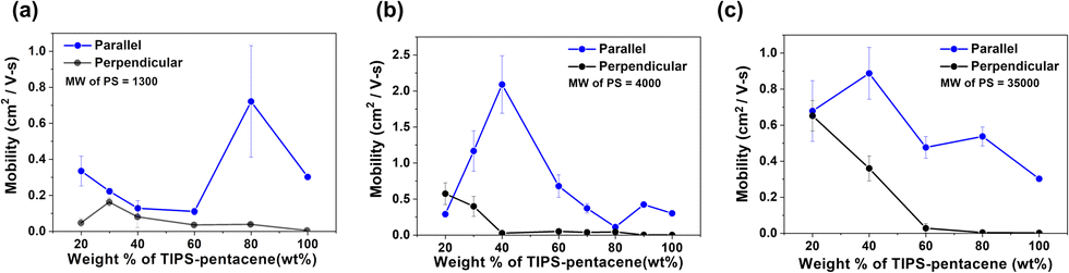 | ||
| Fig. 3 Saturation mobilities of TIPS-pentacene/PS binary films with different molecular weights of PS: (a) 1300, (b) 4000, and (c) 35000. | ||
Blended TIPS-pentacene films with heavier PS polymer (MW = 4000) present morphological trends similar to binary films with lighter PS polymer (MW = 1300). As the weight percentage of TIPS-pentacene decreases in the mixture solution, the anisotropic crystallinity of the TIPS-pentacene films disappears, and the spherulite crystal structure readily forms. However, films still have a constant direction up to 40 wt% through the AFM image, as illustrated in Fig. S7 (ESI†). Charge mobility values are not noticeably improved until the weight ratio of TIPS-pentacene reaches 60 wt%. At a weight ratio of 40 wt%, the charge mobility has the highest value of 1.215 cm2 V−1 s−1, four times higher than that of pure TIPS-pentacene films (Fig. 3b). The change in electrical properties by the device configuration is shown in in Fig. S8 (ESI†).
Fig. 3c illustrates the charge mobility of TIPS-pentacene/PS binary films with the highest molecular weight of PS (MW = 35000). The change in electrical mobilities is negligible due to the high molecular interaction of PS molecules in TIPS-pentacene films. The surface morphologies and electrical properties of TIPS-pentacene/PS (MW = 35000) binary films are presented in Fig. S9 and S10 (ESI†). The spherulite crystal structure of TIPS-pentacene is detected by adding a small amount of PS polymer (even at 80 wt% of TIPS-pentacene). The anisotropic crystallinity of TIPS-pentacene films disappears, and the spherulite crystal structure is readily formed. The blended film with the heaviest PS polymer (MW = 400000) was also attempted, but the improvement in charge mobility was not identical due to its poor solubility, miscibility, and high molecular interaction of PS molecules.
TIPS-pentacene/PS blend analysis
Fig. 4a and b depicts the optical images and transfer curves of TIPS-pentacene/PS (MW = 4000) binary films with 40 wt% and 100 wt% of TIPS-pentacene, respectively, to demonstrate the optical and electrical differences with the PS polymer addition. Pure TIPS-pentacene films present a needle-like 1D crystal structure parallel to the bar-coating direction. However, with the addition of PS polymer, TIPS-pentacene spherulite structured films with connected grains are confirmed. Additionally, films with a weight ratio of 40 wt% exhibit a high on–off ratio and small threshold voltage compared to pure TIPS-pentacene films (Fig. 4c and d). Therefore, the transfer curves indicate that TIPS-pentacene/PS (MW = 4000) binary films are electrically favorable compared to pure films.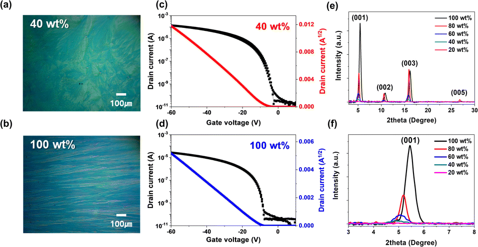 | ||
| Fig. 4 Surface optical images of TIPS-pentacene/PS (MW = 4000) binary films at (a) 40 wt% and (b) 100 wt% of TIPS-pentacene. Transfer curve of TIPS-pentacene/PS (MW = 4000) binary films at (c) 40 wt% and (d) 100 wt% of TIPS-pentacene. (e) X-ray diffraction (XRD) patterns of TIPS-pentacene/PS (MW = 4000) binary films with different wt% ratios of TIPS-pentacene. (f) Magnified XRD patterns for (001) lattice. | ||
The crystallographic information and crystal spacing of blended films were studied using XRD analysis. The XRD peak (001) of TIPS-pentacene can be related to intermolecular interaction along the vertical direction, c-axis, of TIPS-pentacene.25–27 As the weight ratios of TIPS-pentacene decrease, the XRD intensity decreases, indicating that the crystallinity of the blended films decreases within the negligible thickness difference (Fig. 4e and S7†). Specifically, pure TIPS-pentacene films exhibit a peak intensity almost 30 times higher than blended films with the weight ratio of 40 wt%. The intensity decrease in the XRD measurement for TIPS-pentacene can be strongly considered direct evidence of 2D-like spherulite crystal formation.28
Moreover, the PS molecules are well blended with TIPS-pentacene molecules. This is because the molecule distance between TIPS-pentacene is increased from 16.2 Å to 18.0 Å when the PS molecules are added. This is because the PS molecules can be located between each TIPS-pentacene molecule (Fig. 4f and Table S1†). These results caused by the introduction of strain in the crystal after film deposition. Further, the distance along the (001) c-axis increases due to the inserted PS molecules indicating the favorable alignment of the TIPS-pentacene films. The high surface coverage by spherulite morphology and enlarged c-axis films for blended TIPS-pentacene films are beneficial for improving the charge transfer and mobility of FETs.
The miscibility of PS molecules on TIPS-pentacene films can be calculated using the Flory–Huggins theory.29,30 The solubility of each substance in Table S2 (ESI†) and the interaction parameter are calculated to obtain the Flory–Huggins interaction parameter, χ, using the following eqn (1):31
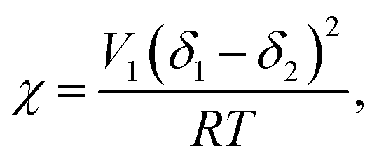 | (1) |
Molecule structural analysis
Polarized UV-visible spectroscopy was used to measure the optical characterization of TIPS-pentacene films and determine the molecule arrangement and direction of charge movement (Fig. 5a and b). Polarized absorption peaks at 695 nm (peak A) indicate long-axis of TIPS-pentacene backbone, and peaks at 445 nm (peak C) indicate the short-axis of TIPS-pentacene backbone.33,34 Polarized absorption peak at 446 nm (peak C) majorly indicates the delocalized carrier transfer along the short-axis of the stacked TIPS-pentacene molecules, which was mainly responsible for the overall electrical performance of the TIPS-pentacene films. Therefore, the direction of transition dipoles along the short-axis of the stacked TIPS-pentacene molecules can be determined by the polarized absorption spectra. Due to the spherulite structure, the peak C of 40 wt% TIPS-pentacene/PS binary films shows the largest intensity when the rotation angles are 0° and 180°, where the direction of transition dipoles and the plane of the organic film channel (coating direction) are parallel (Fig. 5a and c). Instead, for the pure TIPS-pentacene films, according to its needle-like structure, the charge transfer through the short-axis would be dominant when the rotation angle is 30°–60°, which is not parallel to the organic film channel (coating direction) (Fig. 5b and d). Along the carrier channel, the 40 wt% TIPS-pentacene/PS binary films can provide a short and novel route to enhance the overall charge transfer behavior (Fig. S11†).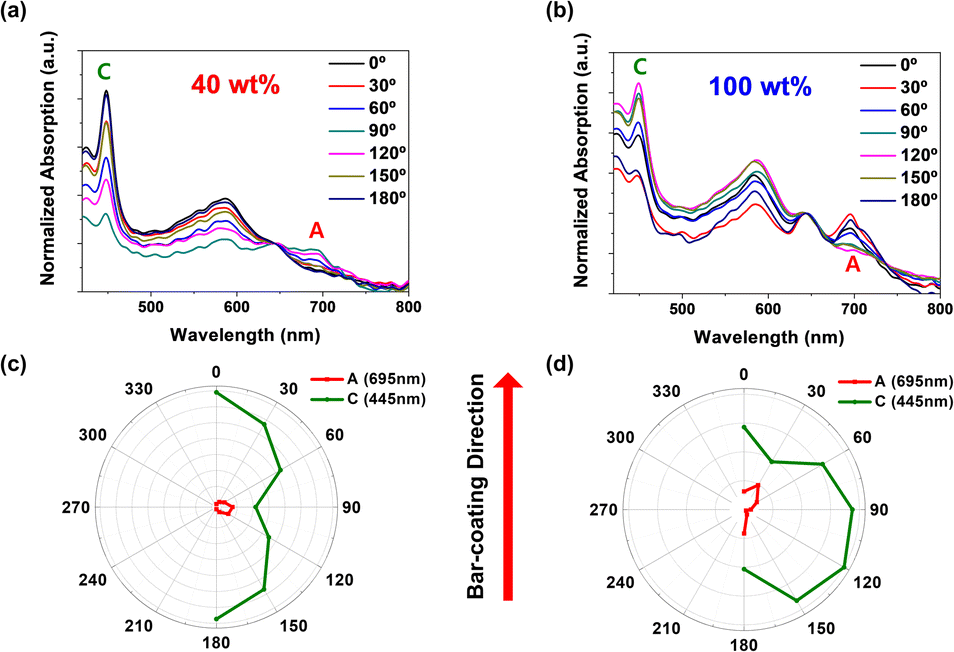 | ||
| Fig. 5 (a and b) Absorption spectra of TIPS-pentacene/PS (MW = 4000) binary films at different weight percentages of TIPS-pentacene. (c and d) Radar plots of the intensity of peak A (695 nm) and peak C (445 nm) with different contact angles. | ||
The charge mobilities of TIPS-pentacene/PS (MW = 4000) binary films at 40 wt% and 100 wt% of TIPS-pentacene were measured by tilting the contact angle from 0° to 180°, as indicated in Fig. 6a. The charge mobility of 40 wt% binary films has the largest value when contact angles are at 0° and 180°, aligning with the polarized optical spectroscopy results. However, for pure TIPS-pentacene films, the highest mobility values are also extracted when Au electrodes are deposited parallel to the bar-coating direction, which does not correspond to the optical measurements.
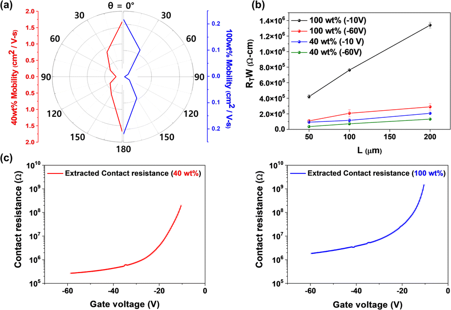 | ||
| Fig. 6 (a) Radar plots for saturation mobilities of TIPS-pentacene/PS (MW = 4000) binary films at 40 wt% and 100 wt% of TIPS-pentacene as a function of the contact angles between the electrode and TIPS-pentacene. (b) Contact resistances by transmission line method according to the weight percentage of TIPS-pentacene and applied voltages in binary films. Extracted contact resistances of TIPS-pentacene/PS (MW = 4000) binary films at (c) 40 wt% and 100 wt% of TIPS-pentacene using a simultaneous extraction model. | ||
According to AFM images, the surface morphology of pure TIPS-pentacene films possesses a twin boundary with 1D structures. Therefore, the charge transition along the short axis region differs from the anticipated arrangement of molecules and crystals within each boundary. In addition, the mobilities of blended films are much greater than those of pure TIPS-pentacene films along all contact angles. For pure TIPS-pentacene films, charge carriers should encounter the interface between crystals as it moves, and the charge mobility should decrease.
Device stability analysis
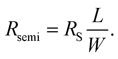
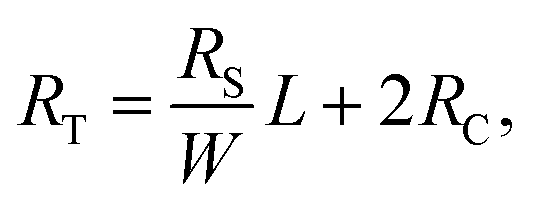
The sample contact resistance was calculated using the transmission line method (TLM) to further understand the electrical improvement of blended films. The TLM measures contact resistance using the structure of the transistor and can be extracted from eqn (2) as follows:35| RT = 2Rm + 2RC + Rsemi, | (2) |
 | (3) |
Rs is calculated sheet resistance of the sample trough the electrical characterization. Subsequently, the total resistance is calculated in eqn (4):
 | (4) |
| Applied voltage [V] | Contact resistance (Ω cm) | |
|---|---|---|
| 100 wt% | 40 wt% | |
| −10 | 141644 |
53069 |
| −60 | 50241 |
5388 |
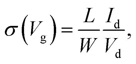
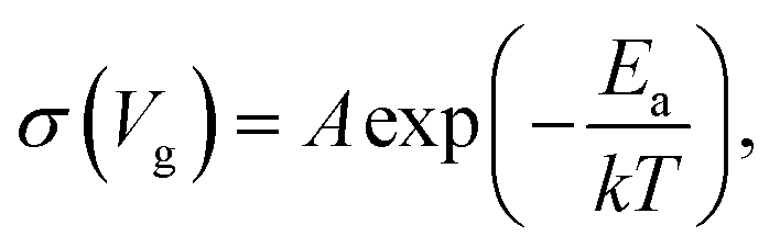
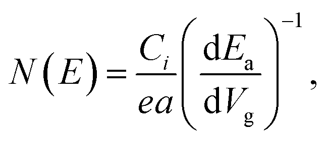
Transfer characteristics were measured at temperatures from 283 K to 113 K with temperature decrements (Fig. S12a and b†). Transistors with pure TIPS-pentacene films exhibited decreasing charge mobility as the temperature decreased, whereas transistors with TIPS-pentacene/PS blended films presented constant charge mobility even when the temperature reached 113 K (Fig. S11c and d†). The trap density of the state was calculated from the transfer curves with different temperatures, suggested by D. V. Lang's method.40 Field-effect conductivity (σ) was plotted using log-scale versus 1/T in Fig. 7a and b, calculated using eqn (5):
 | (5) |
 | (6) |
 | (7) |
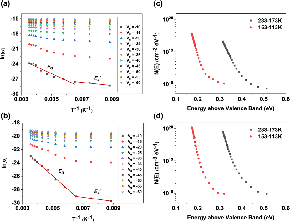 | ||
| Fig. 7 Field-effect conductivity (σ) of TIPS-pentacene/PS (MW = 4000) binary films versus 1/T at (a) 40 wt% and (b) 100 wt% of TIPS-pentacene along Vg. Trap DOS versus energy above the valence band at (c) 40 wt% and (d) 100 wt% of TIPS-pentacene/PS binary films. Extracted contact resistances of TIPS-pentacene/PS (MW = 4000) binary films at (a) 40 wt% and (b) 100 wt% of TIPS-pentacene. Transfer curves of TIPS-pentacene/PS (MW = 4000) binary films at (c) 40 wt% and (d) 100 wt% of TIPS-pentacene at different temperatures. | ||
Conclusions
In this study, TIPS-pentacene and PS blended organic thin-film transistors were fabricated using the bar-coating method. The structure and phase of TIPS-pentacene organic films were controlled using insulating polymer PS and bar-coating procedures. The TIPS-pentacene organic films were managed systematically using variable fabrication parameters, such as the solution concentration, coating speed, PS weight percentage, and contact angles. The surface structures of TIPS-pentacene/PS (MW = 4000) blend films exhibit spherulite structures when the TIPS-pentacene ratio decreases by up to 40 wt%. Moreover, the increased c-axis distance of TIPS-pentacene layers also resulted from the bar-coating method. Optimized TIPS-pentacene organic films present high electrical mobility of up to 1.215 cm2 V−1 s−1, four times higher for pure TIPS-pentacene. The improvement is strongly attributed to the morphology and molecular stacking of TIPS-pentacene, inducing favorable charge transfer conditions. These findings demonstrate a promising strategy for blending organic materials to develop high-performance organic devices using bar-coating methods.Conflicts of interest
The authors declare that they have no known competing financial interests or personal relationships that could appear to influence the work reported in this paper.Acknowledgements
This work was supported by the National Research Foundation of Korea (NRF) funded by the Ministry of Science and ICT (2022R1A5A7000765), Republic of Korea.References
- S. Allard, M. Forster, B. Souharce, H. Thiem and U. Scherf, Angew. Chem., Int. Ed., 2008, 47, 4070–4098 CrossRef CAS PubMed.
- A. Tavasli, B. Gurunlu, D. Gunturkun, R. Isci and S. Faraji, Electronics, 2022, 11, 316 CrossRef CAS.
- S. Riera-Galindo, F. Leonardi, R. Pfattner and M. Mas-Torrent, Adv. Mater. Technol., 2019, 4, 1900104 CrossRef CAS.
- J. H. Lee, Y. Seo, Y. D. Park, J. E. Anthony, D. H. Kwak, J. A. Lim, S. Ko, H. W. Jang, K. Cho and W. H. Lee, Sci. Rep., 2019, 9, 21 CrossRef PubMed.
- Z. He, Z. Zhang, K. Asare-Yeboah, S. Bi, J. Chen and D. Li, Polymers, 2021, 13, 402 CrossRef CAS PubMed.
- W. H. Lee and Y. D. Park, Polymers, 2014, 6, 1057–1073 CrossRef.
- V. Raghuwanshi, D. Bharti, A. K. Mahato, I. Varun and S. P. Tiwari, Synth. Met., 2018, 236, 54–60 CrossRef CAS.
- J. Yang, Z. Zhao, S. Wang, Y. Guo and Y. Liu, Chem, 2018, 4, 2748–2785 CAS.
- D. Guo, Y. Tsai, T. Yu and W. Lee, J. Mater. Chem. C, 2018, 6, 12006–12015 RSC.
- M. Xiao, B. Kang, S. B. Lee, L. M. Perdigão, A. Luci, D. A. Warr, S. P. Senanayak, M. Nikolka, M. Statz and Y. Wu, Adv. Mater., 2020, 32, 2000063 CrossRef CAS PubMed.
- G. Giri, S. Park, M. Vosgueritchian, M. M. Shulaker and Z. Bao, Adv. Mater., 2014, 26, 487–493 CrossRef CAS PubMed.
- M. D. Weber, M. Adam, R. R. Tykwinski and R. D. Costa, Adv. Funct. Mater., 2015, 25, 5066–5074 CrossRef CAS.
- Y. Deng, Q. Wang, Y. Yuan and J. Huang, Mater. Horiz., 2015, 2, 578–583 RSC.
- Y. Deng, E. Peng, Y. Shao, Z. Xiao, Q. Dong and J. Huang, Energy Environ. Sci., 2015, 8, 1544–1550 RSC.
- M. J. Lee, D. Gupta, N. Zhao, M. Heeney, I. McCulloch and H. Sirringhaus, Adv. Funct. Mater., 2011, 21, 932–940 CrossRef CAS.
- F. Paulus, J. U. Engelhart, P. E. Hopkinson, C. Schimpf, A. Leineweber, H. Sirringhaus, Y. Vaynzof and U. H. Bunz, J. Mater. Chem. C, 2016, 4, 1194–1200 RSC.
- K. Haase, C. Teixeira da Rocha, C. Hauenstein, Y. Zheng, M. Hambsch and S. C. Mannsfeld, Adv. Electron. Mater., 2018, 4, 1800076 CrossRef.
- Z. He, J. Chen and D. Li, J. Vac. Sci. Technol., A, 2019, 37, 040801 CrossRef.
- B. Shao, Y. Liu, X. Zhuang, S. Hou, S. Han, X. Yu and J. Yu, J. Mater. Chem. C, 2019, 7, 10196–10202 RSC.
- D. Bharti and S. P. Tiwari, Synth. Met., 2016, 221, 186–191 CrossRef CAS.
- C. Kim, A. Jo, H. Kim, M. Kim, J. Lee and M. J. Lee, J. Korean Ceram. Soc., 2016, 53, 411–416 CrossRef CAS.
- A. Tracz, T. Pakula and J. K. Jeszka, Mater. Sci., 2004, 22, 415–421 CAS.
- S. Lee, S. Kang, G. Jo, M. Choe, W. Park, J. Yoon, T. Kwon, Y. Ho Kahng, D. Kim and B. Hun Lee, Appl. Phys. Lett., 2011, 99, 178 Search PubMed.
- Y. Yunus, N. A. Mahadzir, M. N. Mohamed Ansari, T. Abd Aziz, T. Hasnan, A. Mohd Afdzaluddin, H. Anwar, M. Wang and A. G. Ismail, Polymers, 2022, 14, 1112 CrossRef CAS PubMed.
- G. Rigas, M. M. Payne, J. E. Anthony, P. N. Horton, F. A. Castro and M. Shkunov, Nat. Commun., 2016, 7, 13531 CrossRef CAS PubMed.
- J. Chang, C. Chi, J. Zhang and J. Wu, Adv. Mater., 2013, 25, 6442–6447 CrossRef CAS PubMed.
- N. Shioya, R. Murdey, K. Nakao, H. Yoshida, T. Koganezawa, K. Eda, T. Shimoaka and T. Hasegawa, Sci. Rep., 2019, 9, 1–7 CrossRef CAS PubMed.
- M. Inoue and I. Hirasawa, J. Cryst. Growth, 2013, 380, 169–175 CrossRef CAS.
- P. J. Flory, J. Chem. Phys., 1942, 10, 51–61 CrossRef CAS.
- M. L. Huggins, J. Am. Chem. Soc., 1942, 64, 1712–1719 CrossRef CAS.
- S. J. Lee, Y. Kim, S. Y. Yeo, E. Lee, H. S. Lim, M. Kim, Y. Song, J. Cho and J. A. Lim, Sci. Rep., 2015, 5, 14010 CrossRef PubMed.
- S. Y. Cho, J. M. Ko, J. Jung, J. Y. Lee, D. H. Choi and C. Lee, Org. Electron., 2012, 13, 1329–1339 CrossRef CAS.
- D. T. James, B. C. Kjellander, W. T. Smaal, G. H. Gelinck, C. Combe, I. McCulloch, R. Wilson, J. H. Burroughes, D. D. Bradley and J. Kim, ACS Nano, 2011, 5, 9824–9835 CrossRef CAS.
- D. T. James, J. M. Frost, J. Wade, J. Nelson and J. Kim, ACS Nano, 2013, 7, 7983–7991 CrossRef CAS.
- K. Sakamoto, J. Ueno, K. Bulgarevich and K. Miki, Appl. Phys. Lett., 2012, 100, 75 CrossRef.
- H. Ishii, K. Sugiyama, E. Ito and K. Seki, Adv. Mater., 1999, 11, 605–625 CrossRef CAS.
- H. Sun, Y. Yin, Q. Wang, Q. Jun, Y. Wang, K. Tsukagoshi, X. Wang, Z. Hu, L. Pan and Y. Zheng, Appl. Phys. Lett., 2015, 107, 053304 CrossRef.
- F. Jianfeng, C. Xiaoman, B. Xiao, Z. Lingcheng, J. Jing and W. Feng, J. Semicond., 2014, 35, 064004 CrossRef.
- R. Di Pietro, D. Venkateshvaran, A. Klug, E. J. List-Kratochvil, A. Facchetti, H. Sirringhaus and D. Neher, Appl. Phys. Lett., 2014, 104, 193501 CrossRef.
- D. Lang, X. Chi, T. Siegrist, A. Sergent and A. Ramirez, Phys. Rev. Lett., 2004, 93, 086802 CrossRef CAS PubMed.
Footnotes |
| † Electronic supplementary information (ESI) available. See DOI: https://doi.org/10.1039/d2ra05924j |
| ‡ These authors contributed equally to this work. |
| This journal is © The Royal Society of Chemistry 2023 |