
 Open Access Article
 This Open Access Article is licensed under a Creative Commons Attribution-Non Commercial 3.0 Unported Licence
Cross-linking strategies for hole transport/emissive layers in quantum-dot light-emitting diodes
Yuan-Qiu-Qiang
Yi
 *ab and
Wenming
Su
*a
*ab and
Wenming
Su
*a
aPrintable Electronics Research Center, Nano-Devices and Materials Division, Suzhou Institute of Nano-Tech and Nano-Bionics, Chinese Academy of Sciences, Suzhou 215123, Jiangsu, China. E-mail: yqqyi2020@sinano.ac.cn; wmsu2008@sinano.ac.cn
bpi-Conjugated Polymers Unit, Okinawa Institute of Science and Technology, 1919-1 Tancha, Onna-son, Kunigami-gun, Okinawa 904-0495, Japan
First published on 15th September 2023
Abstract
Due to their excellent features of high efficiency, stability, and high color purity, quantum-dot light-emitting diodes (QD-LEDs) are considered to have great potential as next-generation display technologies. A device should consist of multi-color pixel arrays and corresponding subpixels to fulfill the requirements for high-resolution (HR) QD-LED display panels. Due to the intrinsic solution processability of core–shell structured QDs, the fabrication processes for multi-pixelated HR QD-LED panels are usually transfer printing, inkjet printing (IJP), or photolithography. To avoid the interlayer erosion challenge in the IJP process and direct patterning process of the QD emissive layer (EML), cross-linking strategies have been introduced to construct solvent-resistant films (hole transport layers or QD EMLs) upon exposure to heat or light. This review introduces the recent progress of cross-linking strategies used in hole transport/QD layers of QD-LEDs. Specifically, we present the fundamental chemistries of these cross-linking strategies. We also discuss how these cross-linking methods have been investigated in solution-processed QD-LED devices, especially for IJP/photolithography-based HR QD-LEDs.
Introduction
Display devices are indispensable in our daily life for obtaining visual information.1,2 With the rapid development of augmented/mixed/virtual reality display technologies, the requirements for high-resolution (HR) display devices have also significantly increased with higher standards.3–9 Among different self-emissive technologies, quantum dot (QD) light-emitting diodes (LEDs) are thought to be one of the most promising candidates for HR LED displays, mainly due to their excellent features of tunable spectrum, high color purity, fast response, low energy consumption, and high efficiency.10,11 The inherent core–shell structure and abundant surface ligands of colloidal QD nanocrystals (NCs) have enabled them with cost-effective solution processability for LED fabrications, which also allows for fabricating large-area even flexible electroluminescent (EL) devices.12–14Generally, HR QD-LED displays consist of multi-pixelated arrays, and each pixel unit is typically comprised of subpixels with three primary colors, i.e., red, green, and blue (RGB) QDs. Currently, producing pixel arrays mainly relies on area-selective deposition, transfer printing, inkjet printing (IJP), and photolithography printing.15–19
Among them, IJP technology as a mask-free method has the tremendous advantage of high material utilization, accessible operation, low cost, and individual pixel deposition capabilities, ideally suited to offer high-resolution patterning of large-area films.20–24 However, IJP requires direct deposition of ink droplets onto the underneath layer, which could cause severe interlayer erosion problems and thus deteriorate device performance.25 This raises the challenge of constructing a robust hole transport layer (HTL) against ink solvents. As such, using a thermal or photo cross-linkable HTL became a mainstream choice, which can, once and for all, exhibit full resistance toward various solvents.26,27
In addition to IJP technology, direct photolithography can provide QDs with a fast process toward a patterned emissive layer (EML) with a HR.3,28 Traditionally, photolithography would inevitably use photoresist resins (PRs) while taking complex and lengthy processes to obtain a patterned QD emissive layer and also causing device performance degradation induced by the residual PRs. Direct photo-cross-linking of the QD concept would significantly make the patterning process free of PRs, benefitting from fewer process steps and enabling the QD-LED with a stable device performance.
This review will briefly introduce the various cross-linking strategies behind the construction of solvent-resistant HTLs in IJP QD-LEDs and the photo-induced direct patterning of QD EML with cross-linkers. Also, the fundamental chemistry of these cross-linking strategies will be reviewed.
The fundamental chemistries of cross-linking strategies
One of the most efficient ways to tackle the challenges of interlayer erosion in the IJP process or reduce fabrication process steps for photolithography based QD-LED display panels, is to use a cross-linking strategy to afford the corresponding HTLs or QD layers with solvent resistance. Both the cross-linking strategies share the same fundamental chemistry, adopting thermal or photo-sensitive cross-linkable moieties integrated into their material (HTL or QDs) matrix. The cross-linking functional groups can be categorized into two types, as shown in Fig. 1. The self-cross-linkable moieties, such as vinyl and diacetylene groups, can achieve in situ reactions with each other and thus afford a three-dimensional (3D) cross-linked polymeric network. Alternatively, thanks to the rich aliphatic C–H bond in solution processable hole transport materials (HTMs) and QDs or the carbon–carbon double bond in the surface ligand of QDs, photo-sensitive groups can react with them generating new chemical bonds through carbene, nitrene, or radical mechanisms.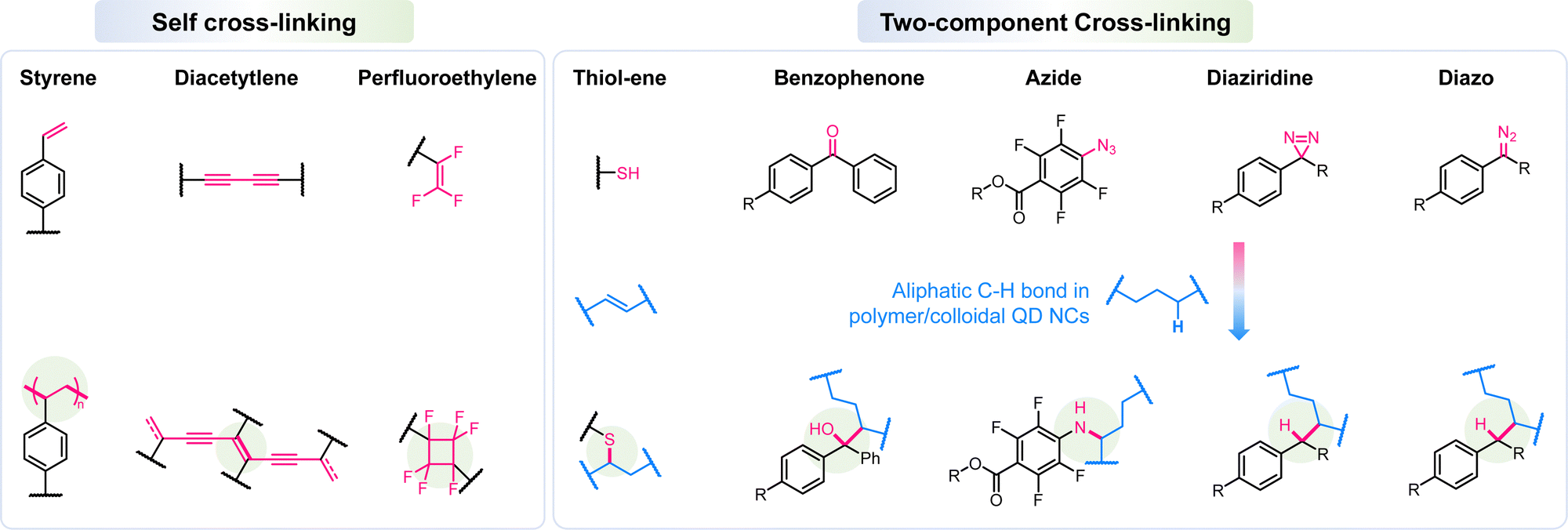 | ||
| Fig. 1 The fundamental chemistries of the current cross-linking strategies used in QD-LEDs. | ||
Cross-linked hole transport layer
Due to the core–shell structure of QDs with abundant surface ligands, one of the most attractive features of QDs is the solution-processability, which can achieve QLED device fabrication at a comparatively low cost and even be compatible with inkjet-printing (IJP) technology for large-area display panels. To date, most of the thin films in QLEDs are solution-processed, which would inevitably cause some interlayer erosion and mixing when coating one material on the underneath one. The interlayer erosion problem can be minimized or even ignored using spin-coating technology with a fast material deposition process. However, when it comes to the IJP-QLEDs, the hole transport layer is usually underneath the emissive QD layer. Considering the comparatively long evaporation process of ink solvents, it is inevitably accompanied by interlayer erosion to the underneath HTL, which could severely damage the HTL morphology to a deteriorated state, thus significantly affecting the QLED performance and stability (Fig. 2).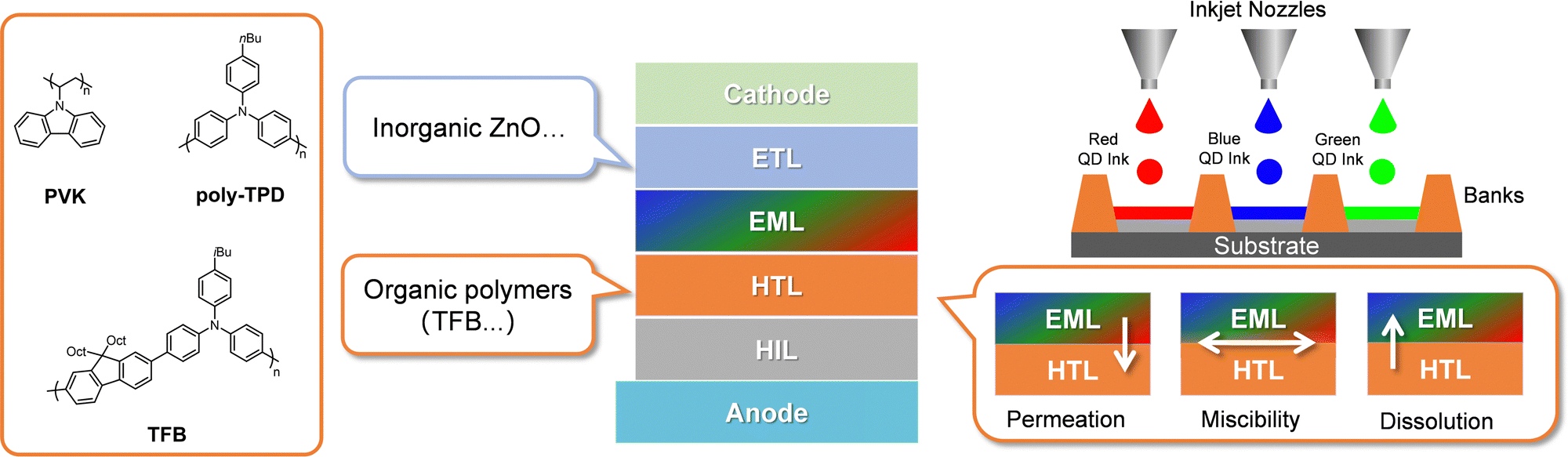 | ||
| Fig. 2 Challenges in solution-processable HTM-based IJP QD-LEDs. | ||
Generally, two methods are available for tackling the interlayer erosion problem between the QD layer and HTL. One is to develop an orthogonal solvent system against the HTL, which is not a universal strategy for all the HTLs and would still bring a considerable challenge for ink formula investigations. The other is to achieve solvent resistance of the HTLs against all common solvents used in the QD ink formula. To achieve solvent resistance of solution-processable HTLs, the in situ cross-linking strategy of the HTL film is the most widely used method, requiring there to be some cross-linkable moieties in their as-cast films.
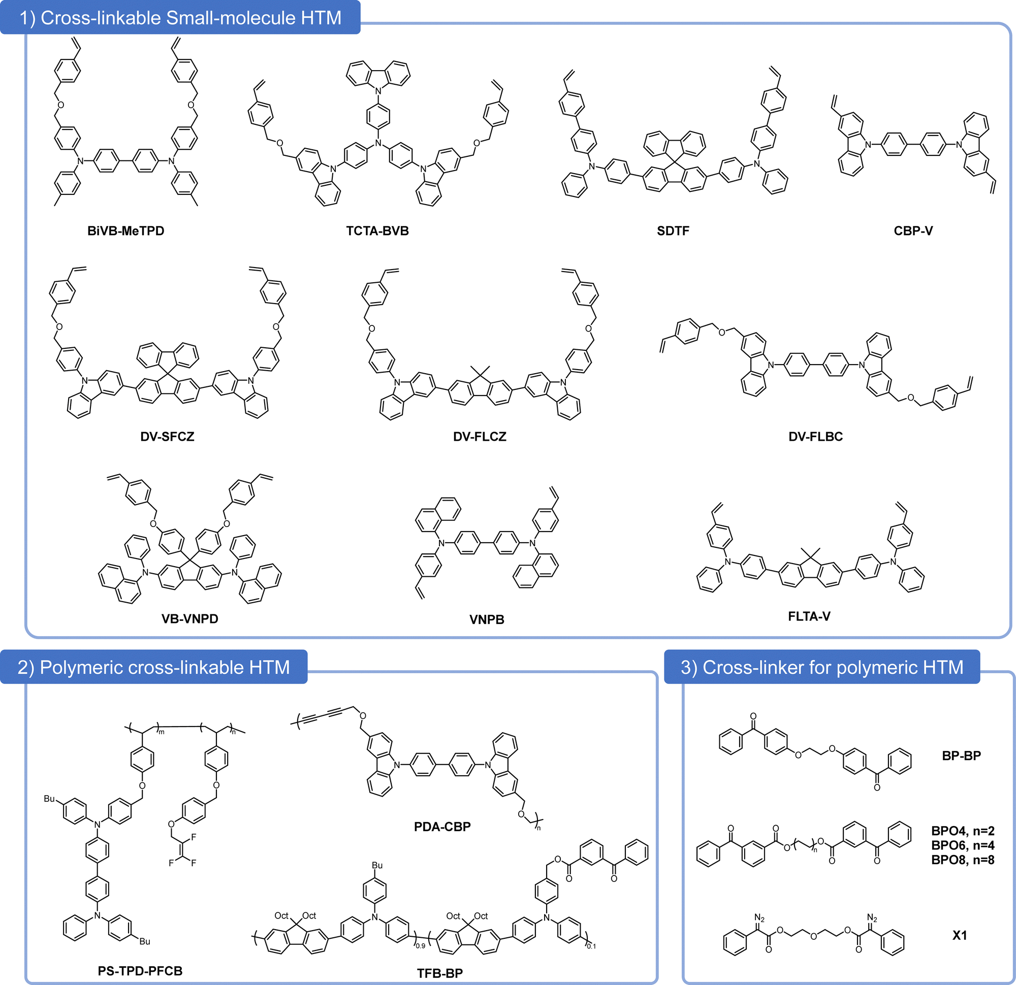
To date, the cross-linking strategy for HTL films can be generally categorized into four types: (1) cross-linkable small-molecule (SM) HTMs, (2) cross-linkable polymeric HTMs, (3) polymeric HTMs blended with cross-linkers, and (4) polymeric HTM blended with the cross-linkable SM-HTM. It should be noted that the strategy core is to use cross-linkable functional groups in SM, which can be stimulated by heat, light, or their combinations, and subsequently form new covalent bonds as in the HTL film.
In addition to the solvent resistance enabled by cross-linking, which is critical in IJP-QLED, there are some other basic requirements for the HTL materials used in the QLED fabrications, such as (1) enough thermal stability with a high glass-transition temperature, (2) matched hole transport mobility with that of the electron transport layer (ETL), (3) a suitable highest occupied molecular orbital (HOMO) level for efficient hole injection and transport, and (4) a shallow lowest unoccupied molecular orbital (LUMO) level for blocking electrons to eliminate excitons formed in the HTL.
Due to the definitive molecular weight and thus without the batch problem, organic SM-HTMs have served as HTLs in QD-LEDs since its early development stage (Fig. 3), such as spiro-N,N′-diphenyl-N,N′-bis(3-methylphenyl)(1,1′-biphenyl)-4,4′-diamine (spiroTPD),29N,N′-bis(3-methylphenyl)-N,N′-bis(phenyl)-benzidine (TPD), N,N′-bis(3-methylphenyl)-N,N′-bis-(phenyl)-9,9-spiro-bifluorene (sp-TPD), and N,N′-bis(naphthalen-1-yl)-N,N′-bis(phenyl)-2,2-dimethylbenzidine (NPD).30 As such, cross-linkable SM-HTMs for QD-LEDs were also developed as early as 2006. Zhao et al. built a double-HTL QD-LED by combining a small-molecule cross-linkable HTM (TCTA-BVB) with a cross-linkable polymeric HTM (PS-TPD-PFCB) to enable cascading HOMO level alignment in the device and therefore a more effective hole transport process.31 Due to the high turn-on voltage and low power efficiency (PE) of this QD-LED, the same group continued to design and synthesize a new thermally cross-linkable HTM, namely BiVB-MeTPD, which improved the EL performance despite a decrease in photoluminescence efficiency (PL).32 The QD-LEDs based on these thermally cross-linkable SM-HTMs showed unsatisfactory device performances, mainly limited by the lack of high-quality QDs and immature device structures in the early development stage of the QD-LEDs.
 | ||
| Fig. 3 Chemical structures of (1) cross-linkable small-molecule HTM, (2) polymeric cross-linkable HTM, and (3) cross-linkers for polymeric HTM. | ||
With the continuing development of QDs and the innovations in the device architecture of QD-LEDs,33–35 the red-green-blue (RGB) QD-LEDs have achieved significant improvements in terms of efficiency and stability, which prompts the industry to consider their applications in display panels. To achieve this goal, there is a need to make RGB pixels efficiently from the QD solutions, in which IJP technology can exactly meet the fabrication requirements to deposit the QD ink into pixels on the substrate directly. However, due to the long evaporation process of ink solvents, the deposition usually causes interfacial erosion and mixing problems. Compared with the use of an orthogonal solvent system, constructing a solvent-resistance HTL from its soluble precursor in the thin film state is a more feasible way to make solution-processable multi-layer QD-LEDs, especially when it comes to IJP QD-LEDs.
In 2017, Xing et al. reported an air-stable thermally cross-linkable HTM for QD-LED, namely N,N′-(9,9′-spirobi[fluorene]-2,7-diylbis[4,1-phenylene])bis(N-phenyl-4′-vinyl[1,1′-biphenyl]-4-amine) (SDTF).36 An IJP QD-LED was successfully fabricated using the cross-linked SDTF with an EQE of 5.54%, slightly better than its spin-coating counterpart. Due to the bulky central core of spiro-fluorene, the cross-linking condition is comparatively harsh, requiring a temperature as high as 230 °C. Considering this, the same group further developed another cross-linkable hole transport material, 4,4′-bis(3-vinyl-9H-carbazol-9-yl)1,1′-biphenyl (CBP-V), which can achieve full resistance to various solvents in a shorter time of 30 minutes.37 A red QD-LED was successfully fabricated by inkjet-printing a CBP-V HTL and QD emissive layer and achieved a maximum EQE of 11.6%, which was 92% of a reference spin-coated QLED (12.6%). However, replacing the central core to a biphenyl group and the active hole transport group to a carbazole successfully deepened the HOMO level of cross-linker CBP-V to −6.2 eV but also caused a high turn-on voltage over 3.2 V in the cross-linked CBP-V based QD-LEDs. A further molecular design was investigated to replace the central unit from spiro-fluorene with less sterically bulky fluorene.38 In combination with the carbazole group, they synthesized two new cross-linkable SM-HTMs: DV-SFCZ and DV-FLCZ. The cross-linking temperature of fluorene based DV-FLCZ is 75 °C lower than that of DV-SFCZ. Notably, the spin-coated RGB QD-LEDs with the cross-linked DV-FLCZ obtained a maximum EQE of 20.5%, 16.6%, and 8.5%, respectively. In order to decrease the cross-linking temperature, a universal synergistic photothermal approach was proposed, dramatically facilitating a drop of 75 °C while maintaining an almost unchanged efficiency.39 In addition to designing new cross-linkable SM-HTMs, borrowing some from organic LEDs also works well in QD-LEDs. For example, the thermally cross-linkable 9,9-bis[4-[(4-ethenylphenyl)methoxy]phenyl]-N2,N7-di-1-naphthalenyl-N2,N7-diphenyl-9H-fluorene-2,7-diamine (VB-FNPD) was introduced to boost the operational stability of QD-LEDs.40 Also, to balance the electron mobility of SM-ETLs, Yang et al. used N4,N4′-Bis(4-ethenylphenyl)-N4,N4′-di-1-naphthalenyl-[1,1′-biphenyl]-4,4′-diamine (VNPB) as the HTL, which favored successful all small-molecule organic transport material-based QD-LEDs.41 Due to the huge successes achieved by TFB in QD-LEDs, Xie et al. reported a cross-linkable 4,4′-(9,9-dimethyl-9H-fluorene-2,7-diyl)bis(N-phenyl-N-(4-vinylphenyl)aniline) (FLTA-V) based on the repeating unit of TFB, facilitating a blue QD-LED with an efficiency of 5.35%.42
To date, many different cross-linking methods have been proposed and applied to constructing solvent-resistant HTLs for QD-LEDs. Though the styrene group-based cross-linkable HTMs show the best performances in all RGB QL-LEDs, the HTMs based on vinyl groups usually accompany the deteriorations during the storage period. This thus would cause huge challenges for fabricating QD-LEDs with consistent performances. There is a need to develop storage stable cross-linkable HTMs for QD-LEDs. Currently, the cross-linkers based on benzophenone and diazo groups, which can achieve in situ cross-linking with polymeric HTL in the thin film state, are comparatively stable for storage and exhibit fairly good device performances. Further molecular design attaching these stable cross-linkable groups would facilitate the synthesis of HTMs with both high performances and long-term storage stability.
Apart from using cross-linkable SM-HTMs, attaching cross-linkable groups on HTL polymer offers another method to achieve fully solvent-resistant HTL. As in the early stage of QD-LED development, Zhao et al. employed a hydrophobic thermally cross-linkable HTL, polystyrene-N,N′-diphenyl-N,N′-bis(4-n-butylphenyl)-(1,1′-biphenyl)4,4′-diamine-perfluorocyclobutane (PS-TPD-PFCB).31 In 2017, Sun et al. designed and synthesized a CBP based polymer using diacetylene as the cross-linkable group, namely 4,4′-bis(3-((prop-2-yn-1-yloxy)methyl)-9H-carbazol-9-yl)-1,1′-biphenyl (PDA-CBP), which exhibited a very low cross-linking temperature of 150 °C.43 Followed by this, they also attached a photosensitive benzophenone group onto the side chain of TFB. They obtained a cross-linkable polymeric HTM (TFB-BP), as shown in Fig. 4(a), and due to the suitable HOMO level around −5.4 eV and high mobility of TFB-BP, the RGB QD-LEDs all achieved a satisfactory EQE of 21.4%, 15.2%, and 8.8%, respectively, which were all higher than their reference TFB ones. With the obtained solvent resistance, an IJP red QD-LED was also fabricated with a highly prestigious EQE of 18.1%.
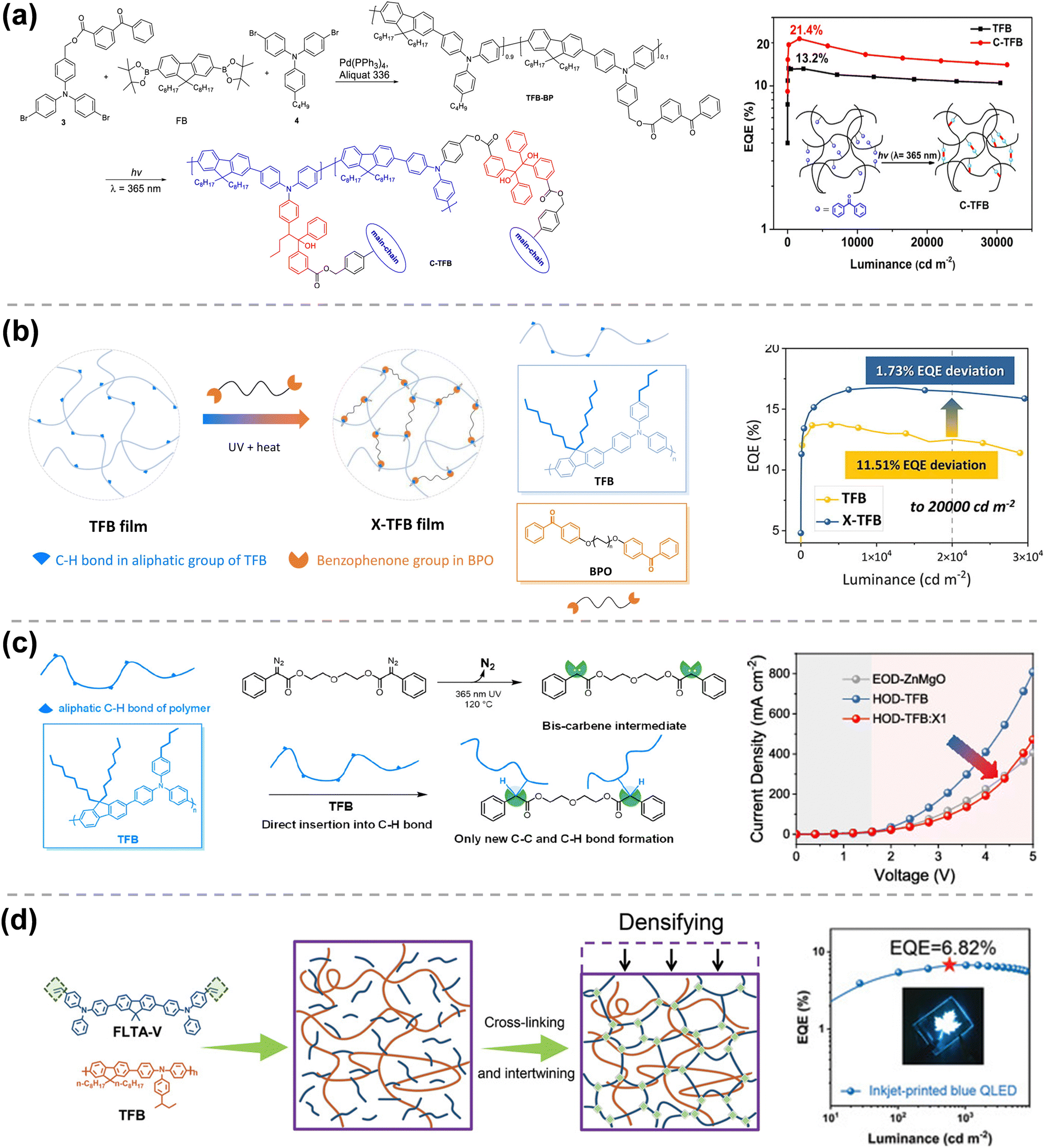 | ||
| Fig. 4 (a) Chemical structure of TBP-BP and its QD-LED. Reprinted with permission from ref. 27. Copyright 2020 American Chemical Society. (b) Cross-linking of TFB and BPO6 under heat and UV. Reprinted with permission from ref. 45. 2022 Elsevier B.V. (c) Reaction mechanism of TFB and X1 based carbene cross-linker. Reprinted with permission from ref. 46. Copyright 2022 American Chemical Society. (d) Intertwined HTL enabled by TFB and cross-linked FLTA-V. Reprinted with permission from ref. 42. Copyright 2022, Wiley-VCH GmbH. | ||
However, the synthesis of cross-linkable polymeric HTM is still very complex. To maintain the high mobility of polymeric HTMs and achieve solvent resistance, the easiest and simplest way is to blend them with small-molecular cross-linkers, which is further responsible for an in situ cross-linking reaction in the film state. In 2017, Zou et al. blended TFB with a photosensitive bifunctional bis-benzophenone (BP–BP), facilitating TFB with full solvent resistance.27 A green QLED device based on cross-linked TFB exhibited an EQE of 8.93%, 1.9-fold higher than that of the pristine TFB based device. In 2002, Yi et al. systematically optimized the chemical structure of benzophenone based cross-linkers (BPO2, BPO4, and BPO8), as shown in Fig. 4(b).45 It was found that BPO6, with a medium central alkyl length, can cross-link with TFB very well to improve the QD-LED performance with the highest EQE of 16.77% (20.22 lm W−1, 22.72 cd A−1), which is 20% higher than that of the pristine TFB based device. An ultra-low EQE deviation of 1.73% was also observed in the cross-linked TFB:BPO6 based red QD-LED. To avoid the generation of free hydroxyl groups after the cross-linking reaction with benzophenone, Yi et al. further developed a bis-diazo compound (X1) as the cross-linker for TFB (Fig. 4(c)). The introduction of X1 into TFB achieved a band structure adjustment, favoring a more balanced charge transport property and, thus, an enhanced device performance.46
Alternatively, blending polymeric HTM with cross-linkable SM-HTM can also make the intertwined HTL with solvent resistance for use in IJP QD-LEDs. In 2020, Tang et al. introduced CBP-V into polymeric TFB, not only affording the solvent resistance but also facilitating a shallower HOMO level to decrease the turn-on voltage of QD-LED.44 With this, the QD-LED realized 22.3% EQE and 7-fold lifetime enhancement compared to the TFB-only device. Also, with the interwined cross-linked HTL, they successfully fabricated an IJP QD-LED with an EQE of up to ∼17%. Recently, Xie et al. blended FLTA-V with TFB (Fig. 4(d)), successfully inkjet printing the blue QDs onto the HTL film and thus delivering a record-high efficiency of 13.4% (18.8 cd A−1, 23.9 lm W−1).42 Besides, CBP-V can also cross-link with highly ordered discotic molecules (T5DP-2,7 and T5PD36) with a superior mobility of ∼2 × 10⁻² cm2 V−1 s−1, forming a cascade energy level within the blue QD-LED device and achieving a high EQE of 18.59% and 18.16%, respectively.47,48 We also summarized the device performances of QD-LEDs using cross-linked HTLs in Table 1.
| Cross-linked HTL | HOMO/LUMO (eV) | PE (lm W−1) | CE (cd A−1) | EQE (%) | Ref. |
|---|---|---|---|---|---|
| PS-TPD-PFCB | −5.3/−2.1 | — | — | 0.4 | 31 |
| PS-TPD-PFCB/TCTA-BVB | −5.7/−2.3 | — | — | 0.8 | 31 |
| BiVB-MeTPD | −5.3/−2.5 | 3.04 | 4.87 | 2.12 | 32 |
| SDTF | −5.5/−2.6 | 15.32 | 22.82 | 5.54 | 36 |
| FLTA-V | −5.6/−2.3 | 4.34 | 5.53 | 6.64 | 42 |
| TFB:FLTA-V | — | 8.42 | 8.26 | 10.20 | 42 |
| DV-SFCZ | −5.7/−2.8 | 18.5 | 25.2 | 16.3 | 38 |
| DV-FLCZ | −5.7/−2.8 | 32.6 | 32.0 | 20.5 | 38 |
| CBP-V | −6.2/−2.9 | 18.1 | 23.9 | 15.0 | 37 |
| PDA-CBP | −5.7/−2.3 | 7.2 | 10.4 | 8.7 | 43 |
| VB-VNPD | −5.3/−2.3 | 32.1 | 32.6 | 8.0 | 40 |
| VNPB | −5.5/−2.4 | 23.9 | 18.8 | 13.4 | 41 |
| TFB-BP | −5.4/−2.5 | 42.3 | 32.3 | 21.4 | 27 |
| TFB:BP-BP | −5.4/−2.5 | 26.22 | 38.83 | 8.93 | 26 |
| TFB:CBP-V | — | 36.8 | 32.8 | 22.3 | 44 |
| TFB:BPO4/BPO6/BPO8 | −5.4/−2.5 | 20.22 | 22.72 | 16.77 | 45 |
| TFB:X1 | −5.5/−2.7 | 22.22 | 29.17 | 14.66 | 46 |
| CBP-V:T5DP-2,7 | −5.8/−2.5 | — | 7.68 | 18.59 | 47 |
It is believed that there is still much room to further enhance the QD-LED performance via engineering cross-linkable HTMs, especially for the IJP ones, by introducing a small-molecule cross-linker into the polymeric HTM matrix. For fabricating IJP QD-LEDs, in addition to the QD ink formula, the surface energy of the cross-linked HTL is another crucial factor needing to be carefully considered, which generally should be over 35 mN m−1. Therefore, constructing a cross-linked HTM with fully solvent resistance and a high surface energy is essential for making IJP QD-LEDs.
Cross-linked and patterned QD emissive layer
Using IJP deposition technology to achieve multi-pixelated arrays in QD-LEDs offers opportunities for low-cost, materials-saving, and large-area fabrications. However, it still needs to be sufficiently mature, especially regarding the restricted resolution (500 pixels per inch (ppi) at the most with the assistance of a bank.4 The direct photolithography of QDs for obtaining a patterned and pixelated emissive layer is another feasible and efficient method, which includes mixing QDs with PRs,49 taking advantage of the electrostatic interaction between the QDs’ surface ligand and the additive organic dyes,50 and regulating the QDs’ solubility by attaching a photosensitive cross-linkable group onto the surface ligand.4,51Compared with the traditional photolithography method using PRs, the photo-cross-linking is a step-wise way to directly achieve a patterned QD emissive layer, as shown in Fig. 5.
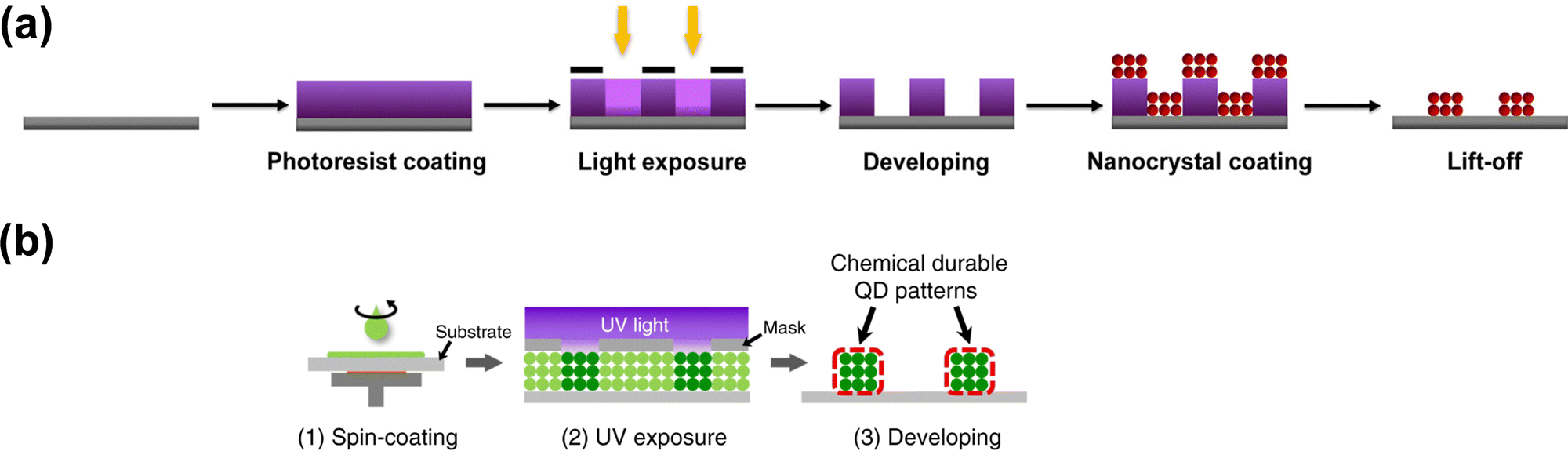 | ||
| Fig. 5 (a) Traditional photolithography method for a patterned QD layer. Reprinted with permission from ref. 52. Copyright 2019 American Chemical Society. (b) Direct photo-cross-linking enabled patterned QD layer. Reprinted with permission from ref. 53. Copyright 2020, Springer Nature. | ||
Regarding introducing photosensitive groups into the surface ligands, this approach is generally enabled by the decomposition51,52,54–56 or cross-linking reaction upon exposure to ultraviolet (UV) light. In this Review, we will mainly introduce the latter method of cross-linking based photolithography for patterned QDs in fabricating LEDs.
As early as 2006, Jun et al. reported a photolithographic process of oleic acid (OA) coordinated CdSeS QDs.61 The reactive double bond in the middle of OA cross-linked with each other when exposed to intense UV light while the unexposed area remained soluble in the toluene solvent. Thanks to this, direct patterns were obtained on the order of 2 μm after UV exposure, followed by solvent rinsing. However, employing this method would cause a shift in the photoluminescence and electroluminescence peaks. X-Ray lithography can also be employed to directly pattern the colloidal perovskite nanocrystals with enhanced stability even in air or water, sharing a similar cross-linking mechanism of generating new intermolecular C![[double bond, length as m-dash]](https://www.rsc.org/images/entities/char_e001.gif) C bonds as shown in Fig. 6(a).
C bonds as shown in Fig. 6(a).
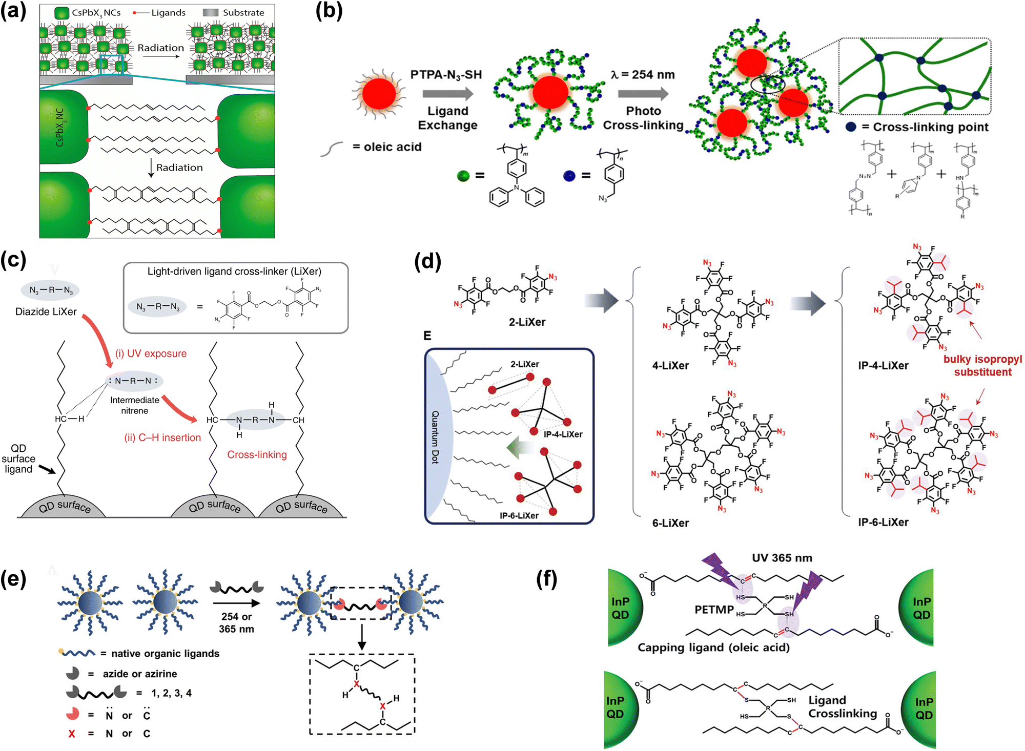 | ||
| Fig. 6 (a) Schematic representation of the irradiation-induced graphitization process. Reprinted with permission from ref. 52. Copyright 2016 American Chemical Society. (b) Schematic illustration of the hybridization of QD with PTPA-N3-SH ligands. Reprinted with permission from ref. 57. Copyright 2020 American Chemical Society. (c) HR patterning of QLEDs via light-driven ligand crosslinking. Reprinted with permission from ref. 53. Copyright 2020, Springer Nature. (d) Chemical structures of n-LiXers and IP-n-LiXers and a schematic describing the limited access of sterically bulky branched n-LiXers to the QD surface. Reprinted with permission from ref. 58. Copyright 2022, Wiley-VCH GmbH. (e) Patterning mechanism. Photogenerated nitrene- and carbene-based crosslinker bridge native ligands on adjacent NCs via C–H insertion. Reprinted with permission from ref. 59. Copyright 2022, Wiley-VCH GmbH. (f) Schematic of the ligand cross-linking procedure between two OA-capped QDs and a PETMP molecule. Reprinted with permission from ref. 60. Copyright 2023, Wiley-VCH GmbH. | ||
In 2020, Ko et al. reported a random copolymeric ligand containing both an azide group and a hole transporting triphenylamine group, poly(vinyltriphenylamine-random-azidostyrene) (P(TPA-r-SN3)-SH), as shown in Fig. 6(b). The cross-linkable azide group can react with the aliphatic C–H bond of the surface ligand of QDs, causing the QD film to no longer be soluble in solvents. The UV induced cross-linking enabled the hybrid QD films without sacrificing the luminescence efficiency and micrometer-scale patterns down to ∼10 μm. Also, the patterned QDs can still be integrated into LEDs with an EQE of 6.25%.57
By employing the widely used photo-cross-linker ethane-1,2-diyl bis(4-azido-2,3,5,6-tetrafluorobenzoate) in semiconducting polymers, Yang et al. successfully achieved the cross-linking reaction of the bis-azide group with their neighboring aliphatic C–H bond on the surface ligand of colloidal QDs upon exposure to UV as depicted in Fig. 6(c).53 After rinsing with solvent, RGB QD patterns with a sub-pixel size of 4 μm × 16 μm can be obtained with a resolution of over 1400 pixels per inch. It should be noted that the bis-azide based cross-linked patterning technology is non-destructive, rendering the QD films with preserved PL and EL performance and affording the QD-LED with an EQE of up to 14.6%. Furthermore, the group modified the chemical structure of the bis-azide cross-linker to four and six-arm azide compounds with multiple cross-linking positions, as shown in Fig. 6(d).58 The cross-linker with bulkier geometry (IP-n-LiXer) can provide an efficient cross-linking reaction with the heavy-metal-free QDs, achieving a minimum feature size down to 1 μm and a high resolution of over 3240 pixels per inch. The crosslinked QD-LEDs further confirmed the effectiveness of n-LiXers for the photolithography of green heavy-metal-free QDs.
Similar to this strategy, Lu et al. reported four bis-azide (nitrene) or bis-diaziridine (carbene) based photo-crosslinkers with varied central units, as shown in Fig. 5(e) and explored their roles of photochemistry in the direct photolithographic patterning of QDs.59 Using UV (i-line, 365 nm) with low doses (<50 MJ cm−2), these designed cross-linkers enable high-fidelity QD patterning, showing a high lateral resolution of ∼3 μm. Compared with the nitrene based cross-linker, the carbene based one exhibited a more appropriate band structure alignment with QDs and a more benign photochemistry during photolithography. The carbene based cross-linker enabled a nondestructive patterned QD film while maintaining 90% of the initial PLQYs. More importantly, the cross-linked QD emissive layer-based LEDs can still feature EQE (11.7%) and a long operating lifetime (T95@1000 nit = 4800 h). Also, the bis-azide cross-linker can be thermally activated and triggered using a laser to facilitate the direct patterning of QDs.62
Recently, by taking advantage of the existing carbon–carbon double bond in the OA surface ligand, Shin et al. reported a thiol–ene click chemistry enabled direct patterning of QD films using the well-established i-line (Fig. 6(f)).60 The formed robust cross-linked QD film exhibited insensitivity to oxygen or water. Furthermore, using the crosslinked InP QDs as the emissive layer, their QD-LED showed a peak CE of 23.04 cd A−1, which was even 158% higher than that of their conventional counterpart.
In addition to blending photosensitive cross-linkers into the QD NCs, Hahm et al. designed and synthesized several simple and versatile benzophenone based photo-cross-linkable ligands (PXLs) as shown in Fig. 7(a) and also devised a dual-ligand passivation system containing PXLs and dispersing ligands (DLs) to guarantee the QDs are universally solution processable for photolithographic patterning techniques (Fig. 7(b)). The dual-ligand cross-linking strategy enabled the direct patterning of QDs on various substrates, compatible with commercialized photolithography (i-line) or inkjet printing technologies with a resolution as high as up to 15![[thin space (1/6-em)]](https://www.rsc.org/images/entities/char_2009.gif) 000 pixels per inch (Fig. 7(c)). With this strategy, a QD-LED array of each primary color was also successfully fabricated (Fig. 7(d)). The dual-ligand passivation enabled cross-linking at no cost to the optical or electrical properties of QDs.
000 pixels per inch (Fig. 7(c)). With this strategy, a QD-LED array of each primary color was also successfully fabricated (Fig. 7(d)). The dual-ligand passivation enabled cross-linking at no cost to the optical or electrical properties of QDs.
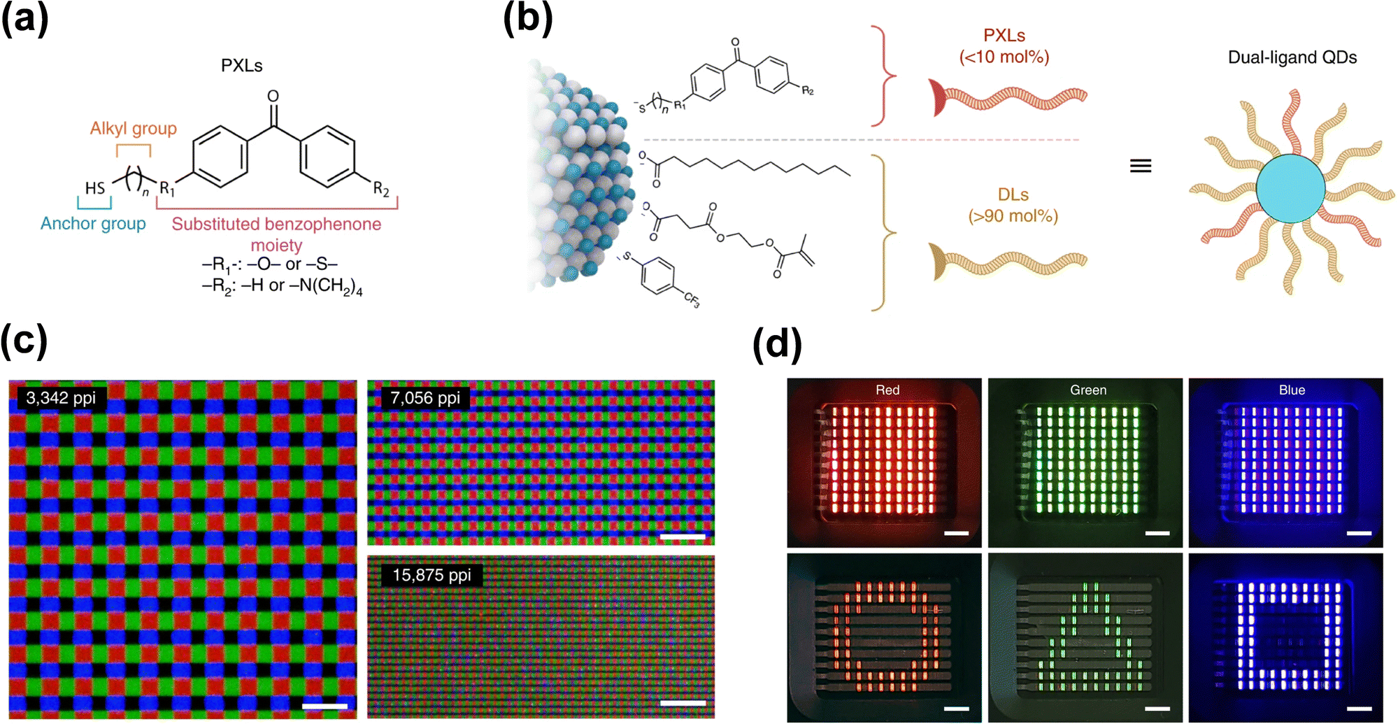 | ||
| Fig. 7 (a) Chemical structure of PXLs. (b) Schematic of dual-ligand QDs. The addition of 1–10mol% PXLs makes QD films become cross-linkable under UV irradiation. The DLs (>90mol%) determine the solubility of QDs. (c) Fluorescent images of RGB QD patterns obtained after consecutive photolithographic processes of primary-colored QDs using an i-line stepper. Scale bars, 10μm. (d) QD-LED array of each primary color. Scale bars, 2mm. Reprinted with permission from ref. 4. Copyright 2020 Springer Nature. | ||
Summary
In summary, we have presented the recent developments in adopting cross-linking strategies for constructing solvent-resistant organic HTLs and photo-induced direct patterning of QD EMLs with cross-linkers, which may have high potential for achieving HR QD-LED display devices using IJP and direct photolithography technologies, respectively.For cross-linked HTLs, these cross-linking strategies have been widely investigated even with better device performance than their uncross-linked counterparts. The cross-linking process can produce a solvent-resistant HTL and fine-tune band structure and film state. However, in addition to these, it is of great importance to achieve a high surface energy when using a cross-linked HTL, which is an essential requirement for the ink droplet spreading well in fabricating IJP QD-LEDs.
For photo-induced photolithography of a QD EML with cross-linkers, huge successes have been achieved in terms of resolutions and device efficiencies. However, the stability of the photo-cross-linking process based QD-LEDs leaves a lot of room for improvement, as the cross-linking process may cause degradation to the inherent characteristics of QDs. The cross-linkers or cross-linkable surface ligands for QDs should be further rationally designed to enhance both efficiency and stability.
Conflicts of interest
The authors declare that they have no known competing financial interests or personal relationships that could have appeared to influence the work reported in this paper.Acknowledgements
This work was financially supported by the National Key Research and Development Program of China (2022YFB3606500) and the Natural Science Foundation of Jiangsu Province (BK20210125).References
- Y. Huang, E. L. Hsiang, M. Y. Deng and S. T. Wu, Mini-LED, Micro-LED and OLED displays: present status and future perspectives, Light Sci Appl, 2020, 9, 105 CrossRef CAS PubMed.
- S. Y. Bang, Y. H. Suh, X. B. Fan, D. W. Shin, S. Lee, H. W. Choi, T. H. Lee, J. Yang, S. Zhan, W. Harden-Chaters, C. Samarakoon, L. G. Occhipinti, S. D. Han, S. M. Jung and J. M. Kim, Technology progress on quantum dot light-emitting diodes for next-generation displays, Nanoscale Horiz., 2021, 6(2), 68–77 RSC.
- Y. Zheng, Y. Yu, W. Chen, H. Hu, T. Guo and F. Li, High-resolution light-emitting devices for display applications. Science China, Materials, 2023, 66(6), 2128–2145 Search PubMed.
- D. Hahm, J. Lim, H. Kim, J. W. Shin, S. Hwang, S. Rhee, J. H. Chang, J. Yang, C. H. Lim, H. Jo, B. Choi, N. S. Cho, Y. S. Park, D. C. Lee, E. Hwang, S. Chung, C. M. Kang, M. S. Kang and W. K. Bae, Direct patterning of colloidal quantum dots with adaptable dual-ligand surface, Nat. Nanotechnol., 2022, 17(9), 952–958 CrossRef CAS PubMed.
- J. Zhao, L. Chen, D. Li, Z. Shi, P. Liu, Z. Yao, H. Yang, T. Zou, B. Zhao, X. Zhang, H. Zhou, Y. Yang, W. Cao, X. Yan, S. Zhang and X. W. Sun, Large-area patterning of full-color quantum dot arrays beyond 1000 pixels per inch by selective electrophoretic deposition, Nat. Commun., 2021, 12(1), 4603 CrossRef CAS PubMed.
- C. Jiang, L. Mu, J. Zou, Z. He, Z. Zhong, L. Wang, M. Xu, J. Wang, J. Peng and Y. Cao, Full-color quantum dots active matrix display fabricated by ink-jet printing, Sci. Chin. Chem., 2017, 60(10), 1349–1355 CrossRef CAS.
- D. M. Geum, S. K. Kim, C. M. Kang, S. H. Moon, J. Kyhm, J. Han, D. S. Lee and S. Kim, Strategy toward the fabrication of ultrahigh-resolution micro-LED displays by bonding-interface-engineered vertical stacking and surface passivation, Nanoscale, 2019, 11(48), 23139–23148 RSC.
- H. Kawanishi, H. Onuma, M. Maegawa, T. Kurisu, T. Ono, S. Akase, S. Yamaguchi, N. Momotani, Y. Fujita, Y. Kondo, K. Kubota, T. Yoshida, Y. Ikawa, T. Ono, H. Higashisaka, Y. Hirano and S. Anzai, High-resolution and high-brightness full-colour “Silicon Display” for augmented and mixed reality, J. Soc. Inf. Disp., 2020, 29(1), 57–67 CrossRef.
- T. Meng, Y. Zheng, D. Zhao, H. Hu, Y. Zhu, Z. Xu, S. Ju, J. Jing, X. Chen, H. Gao, K. Yang, T. Guo, F. Li, J. Fan and L. Qian, Ultrahigh-resolution quantum-dot light-emitting diodes, Nat. Photonics, 2022, 16(4), 297–303 CrossRef CAS.
- V. I. Klimov, Multicarrier Interactions in Semiconductor Nanocrystals in Relation to the Phenomena of Auger Recombination and Carrier Multiplication, Annu. Rev. Condens. Matter Phys., 2014, 5(1), 285–316 CrossRef CAS.
- Y. E. Panfil, M. Oded and U. Banin, Colloidal Quantum Nanostructures: Emerging Materials for Display Applications, Angew. Chem., Int. Ed., 2018, 57(16), 4274–4295 CrossRef CAS PubMed.
- M. N. Yu, M. H. Saeed, S. F. Zhang, H. Y. Wei, Y. Z. Gao, C. Zou, L. Y. Zhang and H. Yang, Luminescence Enhancement, Encapsulation, and Patterning of Quantum Dots Toward Display Applications, Adv. Funct. Mater., 2022, 32(13), 2109472 CrossRef CAS.
- Z. Yang, M. Gao, W. Wu, X. Yang, X. W. Sun, J. Zhang, H.-C. Wang, R.-S. Liu, C.-Y. Han, H. Yang and W. Li, Recent advances in quantum dot-based light-emitting devices: Challenges and possible solutions, Mater. Today, 2019, 24, 69–93 CrossRef CAS.
- Y. Cheng, H. Wan, T. Liang, C. Liu, M. Wu, H. Hong, K. Liu and H. Shen, Continuously Graded Quantum Dots: Synthesis, Applications in Quantum Dot Light-Emitting Diodes, and Perspectives, J. Phys. Chem. Lett., 2021, 12(25), 5967–5978 CrossRef CAS PubMed.
- Y. Shang and Z. Ning, Colloidal Quantum-dots Surface and Device Structure Engineering for High-performance Light-emitting Diodes, Natl. Sci. Rev., 2017, 4(2), 170–183 CrossRef CAS.
- X. Dai, Y. Deng, X. Peng and Y. Jin, Quantum-Dot Light-Emitting Diodes for Large-Area Displays: Towards the Dawn of Commercialization, Adv. Mater., 2017, 29(14), 1607022 CrossRef PubMed.
- J. Yang, J. Yoo, W. S. Yu and M. K. Choi, Polymer-Assisted High-Resolution Printing Techniques for Colloidal Quantum Dots, Macromol. Res., 2021, 29(6), 391–401 CrossRef CAS.
- J. Yang, M. K. Choi, U. J. Yang, S. Y. Kim, Y. S. Kim, J. H. Kim, D. H. Kim and T. Hyeon, Toward Full-Color Electroluminescent Quantum Dot Displays, Nano Lett., 2021, 21(1), 26–33 CrossRef CAS PubMed.
- Y. Sun, Y. Jiang, X. W. Sun, S. Zhang and S. Chen, Beyond OLED: Efficient Quantum Dot Light-Emitting Diodes for Display and Lighting Application, Chem. Rec., 2019, 19(8), 1729–1752 CrossRef CAS PubMed.
- B. Derby, Inkjet Printing of Functional and Structural Materials: Fluid Property Requirements, Feature Stability, and Resolution, Annu. Rev. Mater. Res., 2010, 40(1), 395–414 CrossRef CAS.
- H. M. Haverinen, R. A. Myllyla and G. E. Jabbour, Inkjet Printed RGB Quantum Dot-Hybrid LED, J. Disp. Technol., 2010, 6(3), 87–89 CAS.
- C. Xiang, L. Wu, Z. Lu, M. Li, Y. Wen, Y. Yang, W. Liu, T. Zhang, W. Cao, S. W. Tsang, B. Shan, X. Yan and L. Qian, High Efficiency and Stability of Ink-jet Printed Quantum Dot Light Emitting Diodes, Nat. Commun., 2020, 11(1), 1646 CrossRef CAS PubMed.
- S. Q. Jia, H. D. Tang, J. R. Ma, S. A. Ding, X. W. Qu, B. Xu, Z. H. Wu, G. Y. Li, P. Liu, K. Wang and X. W. Sun, High Performance Inkjet-Printed Quantum-Dot Light-Emitting Diodes with High Operational Stability, Adv. Opt. Mater., 2021, 9(22), 2101069 CrossRef CAS.
- M. Singh, H. M. Haverinen, P. Dhagat and G. E. Jabbour, Inkjet printing-process and its applications, Adv. Mater., 2010, 22(6), 673–685 CrossRef CAS PubMed.
- X. Xiong, C. Wei, L. Xie, M. Chen, P. Tang, W. Shen, Z. Deng, X. Li, Y. Duan, W. Su, H. Zeng and Z. Cui, Realizing 17.0% External Quantum Efficiency in Red Quantum Dot Light-emitting Diodes by Pursuing the Ideal Inkjet-Printed Film and Interface, Org. Electron., 2019, 73, 247–254 CrossRef CAS.
- Y. Zou, Y. Liu, M. Ban, Q. Huang, T. Sun, Q. Zhang, T. Song and B. Sun, Crosslinked conjugated polymers as hole transport layers in high-performance quantum dot light-emitting diodes, Nanoscale Horiz., 2017, 2(3), 156–162 RSC.
- W. Sun, L. Xie, X. Guo, W. Su and Q. Zhang, Photocross-Linkable Hole Transport Materials for Inkjet-Printed High-Efficient Quantum Dot Light-Emitting Diodes, ACS Appl. Mater. Interfaces, 2020, 12(52), 58369–58377 CrossRef CAS PubMed.
- S. Y. Park, S. Lee, J. Yang and M. S. Kang, Patterning Quantum Dots via Photolithography: A Review, Adv. Mater., 2023, e2300546 CrossRef PubMed.
- P. O. Anikeeva, J. E. Halpert, M. G. Bawendi and V. Bulovic, Quantum dot light-emitting devices with electroluminescence tunable over the entire visible spectrum, Nano Lett., 2009, 9(7), 2532–2536 CrossRef CAS PubMed.
- M. J. Panzer, K. E. Aidala, P. O. Anikeeva, J. E. Halpert, M. G. Bawendi and V. Bulovic, Nanoscale morphology revealed at the interface between colloidal quantum dots and organic semiconductor films, Nano Lett., 2010, 10(7), 2421–2426 CrossRef CAS PubMed.
- J. Zhao, J. A. Bardecker, A. M. Munro, M. S. Liu, Y. Niu, I. K. Ding, J. Luo, B. Chen, A. K. Jen and D. S. Ginger, Efficient CdSe/CdS quantum dot light-emitting diodes using a thermally polymerized hole transport layer, Nano Lett., 2006, 6(3), 463–467 CrossRef CAS PubMed.
- Y. H. Niu, A. M. Munro, Y. J. Cheng, Y. Q. Tian, M. S. Liu, J. L. Zhao, J. A. Bardecker, I. Jen-LaPlante, D. S. Ginger and A. K. Y. Jen, Improved Performance from Multilayer Quantum Dot Light-Emitting Diodes via Thermal Annealing of the Quantum Dot Layer, Adv. Mater., 2007, 19(20), 3371–3376 CrossRef CAS.
- X. Dai, Z. Zhang, Y. Jin, Y. Niu, H. Cao, X. Liang, L. Chen, J. Wang and X. Peng, Solution-processed, High-performance Light-emitting Diodes Based on Quantum Dots, Nature, 2014, 515(7525), 96–99 CrossRef CAS PubMed.
- L. Qian, Y. Zheng, J. Xue and P. H. Holloway, Stable and Efficient Quantum-dot Light-emitting Diodes Based on Solution-processed Multilayer Structures, Nat. Photonics, 2011, 5(9), 543–548 CrossRef CAS.
- Q. Sun, Y. A. Wang, L. S. Li, D. Wang, T. Zhu, J. Xu, C. Yang and Y. Li, Bright, multicoloured light-emitting diodes based on quantum dots, Nat. Photonics, 2007, 1(12), 717–722 CrossRef CAS.
- Z. Xing, J. Zhuang, C. Wei, D. Zhang, Z. Xie, X. Xu, S. Ji, J. Tang, W. Su and Z. Cui, Inkjet-Printed Quantum Dot Light-Emitting Diodes with an Air-Stable Hole Transport Material, ACS Appl. Mater. Interfaces, 2017, 9(19), 16351–16359 CrossRef CAS PubMed.
- L. Xie, X. Xiong, Q. Chang, X. Chen, C. Wei, X. Li, M. Zhang, W. Su and Z. Cui, Inkjet-Printed High-Efficiency Multilayer QLEDs Based on a Novel Crosslinkable Small-Molecule Hole Transport Material, Small, 2019, 15(16), 1900111 CrossRef PubMed.
- W. Zhao, L. Xie, Y.-Q.-Q. Yi, X. Chen, J. Hu, W. Su and Z. Cui, Optimizing the central steric hindrance of cross-linkable hole transport materials for achieving highly efficient RGB QLEDs, Mater. Chem. Front., 2020, 4(11), 3368–3377 RSC.
- Y.-Q.-Q. Yi, W. Zhao, L. Xie, Y. Liu, J. Yang and W. Su, 13.2: Invited Paper: Synergistic photothermal strategy for low-temperature cross-linking of hole transport materials for red QLEDs, SID Int. Symp. Dig. Tech. Pap., 2021, 52(S2), 184–186 CrossRef.
- S.-W. Chao, W.-S. Chen, W.-Y. Hung, Y.-Y. Chen, Y.-M. Lin, K.-T. Wong and P.-T. Chou, Cross-linkable hole transporting layers boost operational stability of high-performance quantum dot light-emitting device, Org. Electron., 2019, 71, 206–211 CrossRef CAS.
- L. Yang, X. Li, Q. Yang, S. Wang, H. Tian, J. Ding and L. Wang, High-Performance Red Quantum-Dot Light-Emitting Diodes Based on Organic Electron Transporting Layer, Adv. Funct. Mater., 2020, 31(6), 2007686 CrossRef.
- L. Xie, J. Yang, W. Zhao, Y. Q. Q. Yi, Y. Liu, W. Su, Q. Li, W. Lei and Z. Cui, High-Performance Inkjet-Printed Blue QLED Enabled by Crosslinked and Intertwined Hole Transport Layer, Adv. Opt. Mater., 2022, 10(21), 2200935 CrossRef CAS.
- W. Sun, Y. Deng, Y. Jin, X. Guo and Q. Zhang, Solvent Resistant Hole-Transporting Thin Films via Diacetylene Cross-Linking and Their Applications in Solution-Processed QLEDs, ACS Appl. Polym. Mater., 2020, 2(8), 3274–3281 CrossRef CAS.
- P. Tang, L. Xie, X. Xiong, C. Wei, W. Zhao, M. Chen, J. Zhuang, W. Su and Z. Cui, Realizing 22.3% EQE and 7-Fold Lifetime Enhancement in QLEDs via Blending Polymer TFB and Cross-Linkable Small Molecules for a Solvent-Resistant Hole Transport Layer, ACS Appl. Mater. Interfaces, 2020, 12(11), 13087–13095 CrossRef CAS PubMed.
- Y.-Q.-Q. Yi, J. Yang, L. Xie, Y. Liu, W. Su and Z. Cui, Linear cross-linkers enabling photothermally cured hole transport layer for high-performance quantum dots light-emitting diodes with ultralow efficiency roll-off, Chem. Eng. J., 2022, 439, 135702 CrossRef CAS.
- Y.-Q.-Q. Yi, D. Qi, H. Wei, L. Xie, Y. Chen, J. Yang, Z. Hu, Y. Liu, X. Meng, W. Su and Z. Cui, Molecular Design of Diazo Compound for Carbene-Mediated Cross-Linking of Hole-Transport Polymer in QLED with Reduced Energy Barrier and Improved Charge Balance, ACS Appl. Mater. Interfaces, 2022, 14(34), 39149–39158 CrossRef CAS PubMed.
- X. Zhang, D. Li, Z. Zhang, H. Liu and S. Wang, Constructing Effective Hole Transport Channels in Cross-Linked Hole Transport Layer by Stacking Discotic Molecules for High Performance Deep Blue QLEDs, Adv. Sci., 2022, e2200450 CrossRef PubMed.
- Z. Zhang, X. Zhang, H. Liu, H. Bao, F. Zhang, S. Wang and X. Li, Building one-dimensional hole transport channels in cross-linked polymers to enable efficient deep blue QLED, Chem. Eng. J., 2023, 451, 138516 CrossRef CAS.
- K. Um, H.-J. Kim, J. H. Jo, H. Jeon, H.-B. Yang, Y.-J. Kim and K. Lee, Enhancing efficiency of quantum dot/photoresist nanocomposite using wrinkled silica-quantum dot hybrid particles, Chem. Eng. J., 2019, 369, 109–115 CrossRef CAS.
- G. Devatha, A. Rao, S. Roy and P. P. Pillai, Förster Resonance Energy Transfer Regulated Multicolor Photopatterning from Single Quantum Dot Nanohybrid Films, ACS Energy Lett., 2019, 4(7), 1710–1716 CrossRef CAS.
- Y. Wang, I. Fedin, H. Zhang and D. V. Talapin, Direct optical lithography of functional inorganic nanomaterials, Science, 2017, 357(6349), 385–388 CrossRef CAS PubMed.
- Y. Wang, J. A. Pan, H. Wu and D. V. Talapin, Direct Wavelength-Selective Optical and Electron-Beam Lithography of Functional Inorganic Nanomaterials, ACS Nano, 2019, 13(12), 13917–13931 CrossRef CAS PubMed.
- J. Yang, D. Hahm, K. Kim, S. Rhee, M. Lee, S. Kim, J. H. Chang, H. W. Park, J. Lim, M. Lee, H. Kim, J. Bang, H. Ahn, J. H. Cho, J. Kwak, B. Kim, C. Lee, W. K. Bae and M. S. Kang, High-resolution patterning of colloidal quantum dots via non-destructive, light-driven ligand crosslinking, Nat. Commun., 2020, 11(1), 2874 CrossRef CAS PubMed.
- H. Cho, J. A. Pan, H. Wu, X. Lan, I. Coropceanu, Y. Wang, W. Cho, E. A. Hill, J. S. Anderson and D. V. Talapin, Direct Optical Patterning of Quantum Dot Light-Emitting Diodes via In Situ Ligand Exchange, Adv. Mater., 2020, 32(46), e2003805 CrossRef PubMed.
- J. A. Pan, J. C. Ondry and D. V. Talapin, Direct Optical Lithography of CsPbX3 Nanocrystals via Photoinduced Ligand Cleavage with Postpatterning Chemical Modification and Electronic Coupling, Nano Lett., 2021, 21(18), 7609–7616 CrossRef CAS PubMed.
- Y. Wang, X. Shan, Y. Tang, T. Liu, B. Li, P. Jin, K. Liang, D. Li, Y. M. Yang, H. Shen, B. Zhu and B. Ji, Direct Optical Patterning of Nanocrystal-Based Thin-Film Transistors and Light-Emitting Diodes through Native Ligand Cleavage, ACS Appl. Nano Mater., 2022, 5(6), 8457–8466 CrossRef CAS.
- J. Ko, J. H. Chang, B. G. Jeong, H. J. Kim, J. F. Joung, S. Park, D. H. Choi, W. K. Bae and J. Bang, Direct Photolithographic Patterning of Colloidal Quantum Dots Enabled by UV-Crosslinkable and Hole-Transporting Polymer Ligands, ACS Appl. Mater. Interfaces, 2020, 12(37), 42153–42160 CrossRef PubMed.
- J. Yang, M. Lee, S. Y. Park, M. Park, J. Kim, N. Sitapure, D. Hahm, S. Rhee, D. Lee, H. Jo, Y. H. Jo, J. Lim, J. Kim, T. J. Shin, D. C. Lee, K. Kwak, J. S. Kwon, B. Kim, W. K. Bae and M. S. Kang, Nondestructive Photopatterning of Heavy-Metal-Free Quantum Dots, Adv. Mater., 2022, 34(43), e2205504 CrossRef PubMed.
- S. Lu, Z. Fu, F. Li, K. Weng, L. Zhou, L. Zhang, Y. Yang, H. Qiu, D. Liu, W. Qing, H. Ding, X. Sheng, M. Chen, X. Tang, L. Duan, W. Liu, L. Wu, Y. Yang, H. Zhang and J. Li, Adaptable dual: The Role of Photochemistry of Crosslinkers in the Direct Optical Patterning of Colloidal Nanocrystals, Angew. Chem., Int. Ed., 2022, 61(23), e202202633 CrossRef CAS PubMed.
- S. Shin, K. Kang, H. Jang, N. Gwak, S. Kim, T. A. Kim and N. Oh, Ligand-Crosslinking Strategy for Efficient Quantum Dot Light-Emitting Diodes via Thiol-Ene Click Chemistry, Small Methods, 2023, e2300206 CrossRef PubMed.
- S. Jun, E. J. Jang, J. Park and J. Kim, Photopatterned semiconductor nanocrystals and their electroluminescence from hybrid light-emitting devices, Langmuir, 2006, 22(6), 2407–2410 CrossRef CAS PubMed.
- F. Li, C. Chen, S. Lu, X. Chen, W. Liu, K. Weng, Z. Fu, D. Liu, L. Zhang, H. Abudukeremu, L. Lin, Y. Wang, M. Zhong, H. Zhang and J. Li, Direct Patterning of Colloidal Nanocrystals via Thermally Activated Ligand Chemistry, ACS Nano, 2022, 16(9), 13674–13683 CrossRef CAS PubMed.
| This journal is © the Partner Organisations 2023 |