DOI:
10.1039/D2QM01376B
(Research Article)
Mater. Chem. Front., 2023,
7, 1803-1812
Bridging the inter-grain charge transport via organic semiconductors for high-performance thickness-insensitive perovskite solar cells†
Received
31st December 2022
, Accepted 8th March 2023
First published on 9th March 2023
Abstract
The solution-processability of perovskite solar cells (PVSCs) reduces the production cost, but renders a multi-crystalline film with a large number of grain boundaries, which hinders the charge transport and induces defects. In this work, we have studied the potential of organic semiconductors for remedying the grain boundaries of perovskite films. Non-fullerene acceptors (NFAs) of different energy levels have been filled into the grain boundaries of perovskite films to form different energetic structures. It is unveiled that constructing a “flat-band” quantum well structure (FBQW, where the highest occupied molecular orbital and lowest unoccupied molecular orbital align with the valence band and conductance band, respectively), can effectively bridge the charge transport at the grain boundaries. As a result, the NFA, i.e., HFO-PCIC can obviously reduce the series resistance and enable the best device performance of over 21% based on MAPbI3 solar cells. Moreover, constructing a FBQW at the grain boundary almost fully retains the device efficiency (20.7% for the best) with a perovskite thickness over 1500 nm, which is the best result among thick PVSCs. With the thickness-insensitive merit, the fabrication of perovskites will be more tolerant to the processing conditions toward practical application. Therefore, the FBQW proposed in this work can effectively remedy inter-grain charge transport for high device performance and should pave the way for thickness-insensitive perovskite solar cells for future commercialization of PVSCs.
Introduction
Hybrid organic–inorganic metal halide perovskites solar cells (PVSCs) possess exceptional optoelectronic properties, high absorption coefficients, long carrier diffusion lengths, superb charge carrier mobilities, and tunable bandgaps that make them attract paramount interest from the research community.1–10 Up to now, the power conversion efficiency (PCE) of PVSCs with single-junction 3D cells has been dramatically enhanced from 3.8% in 2009 to over 25%, which qualifies it to compete with silicon solar cells in the future PV market.11–16 At the same time, the solution processing of PVSCs offers an additional advantage for fabricating high-efficiency PVSC devices at a low cost. These achievements accelerate the pace of commercialization. However, the solution processing of perovskite film induces a multi-crystalline film, which will produce a large number of grain boundaries in the active layer and unpredictable surface morphology.17,18 Obviously, preparing a perovskite film with good uniformity, pinhole-free texture, and high crystallinity is vital to achieve high performance for PVSCs, because the rough surface and pin-holes of the perovskite active layer will cause a severe leakage current, and the low crystallinity will cause high resistance and low charge collection efficiency.19 Various modification strategies have been proposed to achieve a smooth surface but a high-crystallinity perovskite film, including component engineering, solvent engineering, interface modification, and optimized preparation process.18,20–34
Nevertheless, challenges remain to achieve high-performance PVSCs. On one hand, a large number of defects are inevitably formed at grain boundaries, resulting in serious nonradiative charge recombination and a short carrier life.35–39 As a result, tremendous efforts have been focused on amending the defect states via a variety of strategies, e.g., passivation of surfaces and interfacial defects and passivation of grain boundaries.17,40–47 On the other hand, the grain boundary naturally forms a physical gap for smooth charge transport between grains. This is detrimental to charge collection and causes a low fill factor (FF) and poor PCE, but has been less studied.
The most direct way to alleviate the poor grain boundary-induced charge transport issue is via enlarging the grain size, and ideally, the grain size should be large enough to connect the anode and cathode within one single grain.17,48,49 Therefore, a large grain size comparable or larger than the scale of film thickness is required, and the optimal thickness of the perovskite should be limited by the grain size. However, the critical balance between the high crystallinity and surface smoothness determines the grain size around 500–1000 nm.50 This might be the reason underpinning the limit of perovskite thickness of 500–1000 nm for the optimal devices. However, PVSCs with both high performance and a thick perovskite layer (or good thickness tolerance) are essential for industrial manufacturing with up-scaled fabrication processing, e.g., doctor blade, slot-die, etc., which inevitably cause fluctuation in perovskite thickness.51 To resolve this issue, it is necessary to dwell on the inter-grain charge transport in multi-crystalline perovskite films and increase their carrier transit lengths.26,36,37,52–56 However, few efforts have focused on this, due to the lack of fundamentals on the inter-grain charge transport and the shortage of appropriate strategies to bridge the charge transport.42
In this work, different from common logic of grain boundary passivation to suppress the charge recombination in perovskite films, we focus on remedying the inter-grain charge transport via organic semiconductors to enable thickness-insensitive PVSCs for practical application. We have proposed the concept of a “flat band” quantum well structure (FBQW), that is, the highest occupied molecular orbital (HOMO) and the lowest unoccupied molecular orbital (LUMO) of organic semiconductors are in line with the valence band (VB) and the conductivity band (CB) of the perovskite, respectively, to enable efficient inter-grain charge transport. Non-fullerene acceptors (NFAs) with different energy levels, i.e., HFO-PCIC, HF-PCIC, and OF-PCIC (Fig. 1a), have been blended into perovskite films, and these NFAs are expected to be compelled to the grain boundary during the crystallization of perovskite films.57 We find that the NFAs have an obvious influence on the series resistance (Rs) of solar cells, and the HFO-PCIC achieves the lowest Rs and the best PCE of over 21%. Moreover, PVSCs with a FBQW structure show very good thickness tolerance, and the efficiency is maintained at 20.7% with the thickness exceeding 1500 nm, which represents the best result among thick PVSCs. Our work proposes the concept of a FBQW structure for boosting the inter-grain charge transport and paves the way for the preparation of thickness-insensitive PVSCs for future commercialization.
 |
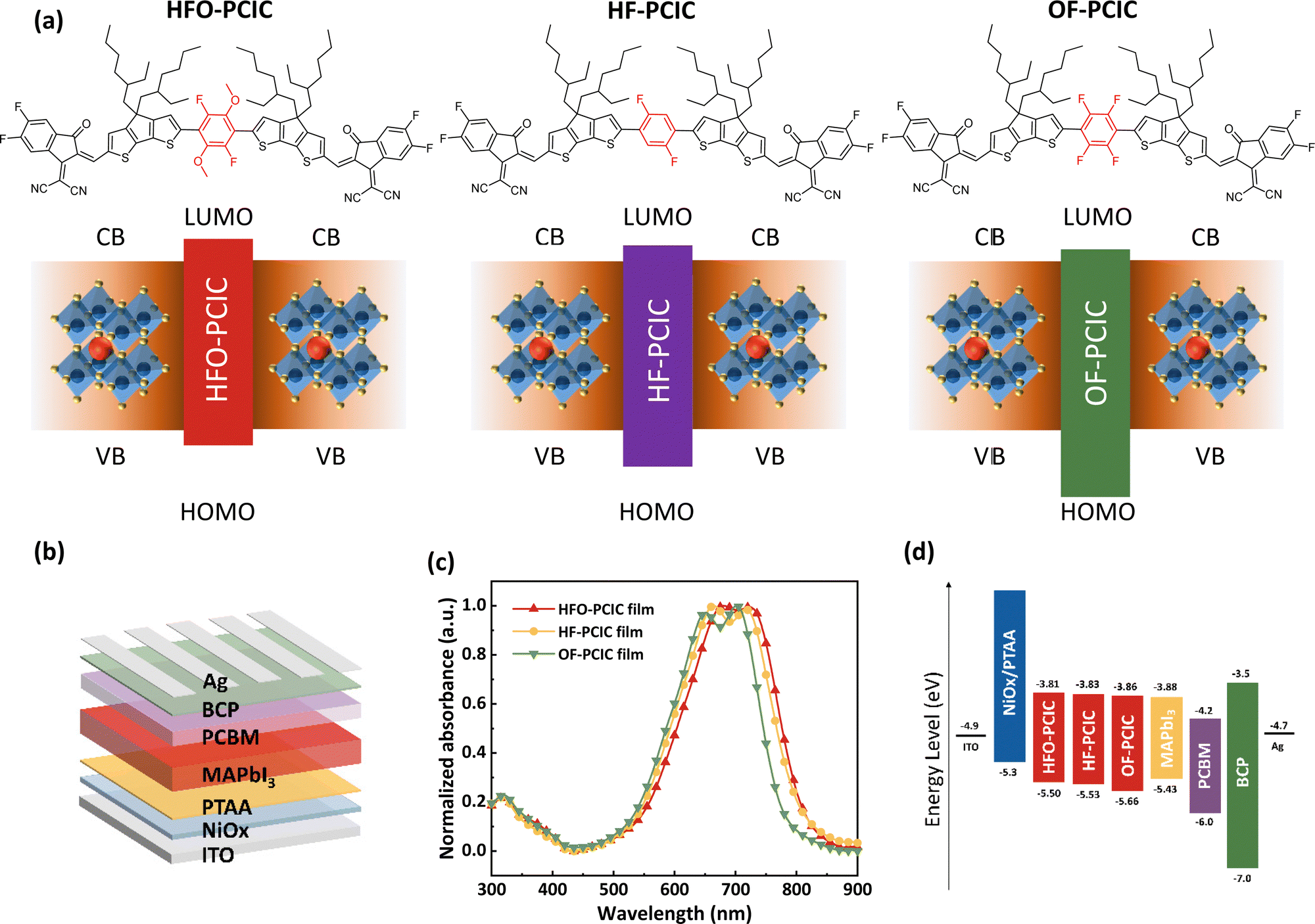
| | Fig. 1 (a) Chemical structures of HFO-PCIC, HF-PCIC, and OF-PCIC. (b) The schematic device structure of a typical MAPbI3 PVSC device. (c) UV-vis absorption spectra of HFO-PCIC, HF-PCIC, and OF-PCIC thin films. (d) The energy level alignment of each layer. | |
Results and discussion
Materials selection
To study the effect of organic semiconductors on device performance, the inverted device structure: glass/indium tin oxide (ITO)/nickel oxide (NiOx)/poly[bis(4-phenyl)(2,4,6-trimethylphenyl)amine] (PTAA)/MAPbI3/[6,6]-phenyl-C61-butyric acid methyl ester (PC61BM)/bathocuproine (BCP)/Ag, was adopted, as shown in Fig. 1b. Considering that the energy level alignment between two semiconductors is the key for charge transfer or charge transport, we focus on exploring the effect of energetic structure across the grain boundary of perovskite film on the device performance. To exclude other effects on the device performance of PVSCs, e.g., morphology, chemical interactions between perovskite and different functional groups,29etc., these molecules should have similar chemical structures but different energy levels, which can be tuned via delicate modification on the side chains or side groups. As a result, we have carefully selected the home-made NFAs, i.e., HFO-PCIC, HF-PCIC and OF-PCIC from a large pool of organic semiconductors.57 As shown in Fig. 1c, the absorbing edges of HFO-PCIC, HF-PCIC, and OF-PCIC are 815 nm, 810 nm, and 780 nm, respectively, which are similar enough to exclude the effect of band gap (Eg, 1.69 eV, 1.70 eV, and 1.80 eV) on the optoelectronic properties. It should be noted that the band gap of these organic semiconductors is quite similar to that of the MAPbI3 perovskite film. With the different side groups, these molecules show different HOMO and LUMO levels, as shown in Fig. 1d. Notably, the HFO-PCIC shows the HOMO at −3.81 eV, and the LUMO at −5.50 eV and these values are quite close to the VB and CB of MAPbI3, respectively.57,58 The HF-PCIC shows overall down-shifted HOMO and LUMO to −3.83 and −5.53 eV, respectively, due to the removal of the electron donating group. The OF-PCIC shows even down-shifted HOMO and LUMO to −3.86 eV and −5.66 eV, respectively. The energy offsets between the LUMO of these NFAs and CB of MAPbI3 perovskite (ΔELUMO-CB) are quite small, i.e., 0.07, 0.05 and 0.02 eV for HFO-PCIC, HF-PCIC and OF-PCIC, respectively. While the energy offsets between the NFA HOMO and VB of perovskite (ΔEHOMO-VB) are large, i.e., 0.07, 0.10, and 0.23 eV for HFO-PCIC, HF-PCIC and OF-PCIC, respectively. It is obvious that these molecules can form different energetic structures with the perovskite at the grain boundary, i.e., the type I quantum well structure with different energy barriers.
Device performance
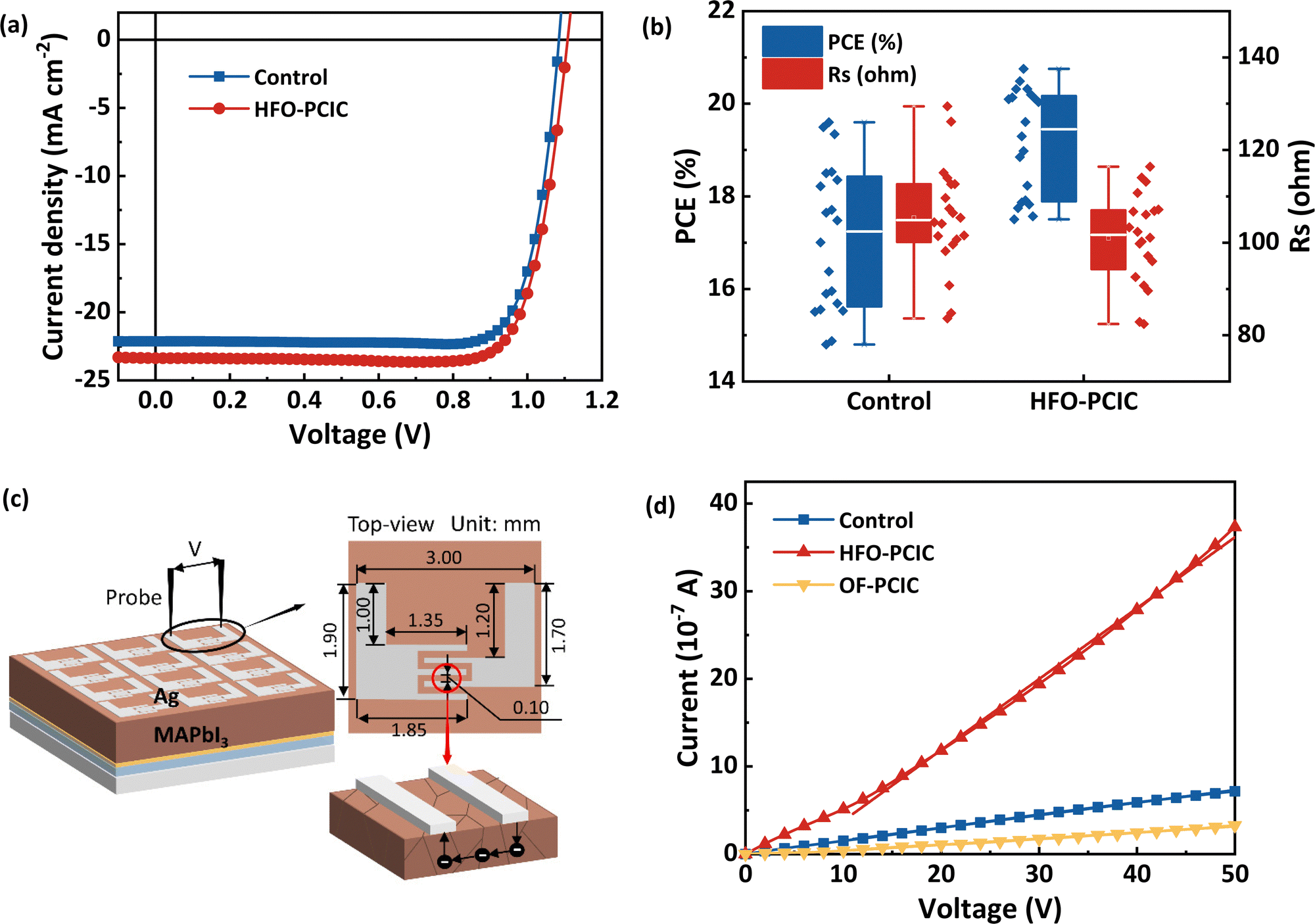
Therefore, these molecules provide a straightforward comparison to test the effect of the energetic barrier of the grain boundary on the device performance of PVSCs. Fig. 2a shows the current–voltage (J–V) of PVSC without or with different NFAs, and the detailed device parameters are summarized in Table 1. The PVSCs without any NFAs (or the control device) reach the best PCE of 20.67% (average PCE: 20.10%), with open circuit voltage (VOC) of 1.08 eV, short circuit current density (JSC) of 22.86 mA cm−2 and fill factor (FF) of 81.55%. With the HFO-PCIC blended into the perovskite film, which shows both small ΔEHOMO-VB and ΔELUMO-CB, the device exhibits the best device performance of 21.19% (average PCE: 20.44%), with a VOC of 1.08 eV, JSC of 23.29 mA cm−2 and FF of 80.88%. With the OF-PCIC blended into the perovskite film, which shows small ΔELUMO-CB but larger ΔEHOMO-VB, the devices show the best device performance of 20.47% (average PCE: 19.94%), with a VOC of 1.08 eV, JSC of 22.94 mA cm−2 and FF of 80.59%. While the device performance of PVSCs with HF-PCIC sits in between that of the OF-PCIC and HFO-PCIC. From the variation trend, it is concluded that the device performance shows an increasing trend with the ΔEHOMO-VB decreasing. These results suggest the interfacial energetic structures indeed play a critical role in determining the device performance of PVSCs. Theoretically, the effect of ΔEHOMO-VB and ΔELUMO-CB on the device performance of PVSCs should be similar. However, considering the ΔELUMO-CB are quite small in all cases, the variation of device performance is attributed to the ΔEHOMO-VB. Interestingly, we find the device stability is increased after NFA modification, as shown in Fig. S6 (ESI†).
 |
| | Fig. 2 (a) J–V characteristics of the control and the NFA-mixed PVSCs. (b) EQE spectra and integrated JSC curves of the control and the NFA-mixed PVSCs. (c) The histogram of ΔEHOMO-VB and Rs. (d) J0.5–V characteristics of hole-only devices, along with linear fits. | |
Table 1 Photovoltaic performances of PVSCs under AM 1.5 G illumination (100 mW cm−2). The average values were obtained from 30 cells
| NFA |
ΔEHOMO-VB (eV) |
V
OC (V) |
J
SC (mA cm−2) |
FF (%) |
R
s (Ω cm−2) |
PCE (%) |
Best PCE (%) |
J
cal (mA cm−2) |
| Control |
0 |
1.08 ± 0.013 |
22.86 ± 0.37 |
81.55 ± 1.52 |
90.26 ± 5.12 |
20.10 ± 0.20 |
20.67 |
22.18 |
| HFO-PCIC |
0.07 |
1.08 ± 0.005 |
23.29 ± 0.25 |
80.88 ± 0.90 |
87.02 ± 5.46 |
20.44 ± 0.29 |
21.19 |
22.83 |
| HF-PCIC |
0.10 |
1.08 ± 0.013 |
23.33 ± 0.25 |
80.18 ± 1.16 |
88.55 ± 8.79 |
20.15 ± 0.43 |
21.09 |
22.20 |
| OF-PCIC |
0.23 |
1.08 ± 0.005 |
22.94 ± 0.34 |
80.59 ± 0.72 |
93.36 ± 6.76 |
19.94 ± 0.34 |
20.47 |
21.79 |
It should be noted that, with the ΔEHOMO-VB increasing from 0.07 to 0.23 eV, JSC shows a decreasing trend. To determine the detailed mechanism underlying the improved charge generation with smaller ΔEHOMO-VB, the external quantum efficiency (EQE) of the PVSCs with and without NFAs is measured, as shown in Fig. 2b. It is observed that with the ΔEHOMO-VB decreasing, the shape of the EQE spectrum shows little change, while the photo-to-electron response increases over the entire range. Besides, we find the UV-visible absorption spectra of the perovskite films without or with different NFAs addition exhibit very small changes, and this excludes the role of absorption on the improved charge generation, as shown in Fig. S1 in the ESI.† Alternatively, these results support the argument that the addition of NFAs majorly increases the charge generation by affecting the carrier dynamic process or the internal quantum efficiency, rather than any optical effect. By integrating the EQE over the AM 1.5G standard spectrum, the JSCs of the control and the PVSCs blended with HFO-PCIC, HF-PCIC, and OF-PCIC are calculated to be 22.18, 22.83, 22.20 and 21.79 mA cm−2, respectively. These results are in accord with the measured JSC under the solar simulator (within 5%), validating the measured device performance as shown in Table 1. It is obvious that lowering the energetic offset at the grain boundary can greatly affect the carrier dynamics of the PVSCs, particularly the charge transport properties.
Charge transport
To further probe the effect of NFA treatment, we carried out steady-state photoluminescence (PL) spectroscopy and time-resolved photoluminescence (TRPL) decay measurements to examine the possible passivation effect. However, as shown in Fig. S5 and Table S4 (ESI†), neither the PL intensity nor the PL life time show any difference with or without the NFA modification. These results exclude the possibility of defect passivation as the mechanism for device performance improvement. As a result, we investigated the effect of NFAs on the charge transport of PVSCs. The Rs is the most direct parameter to examine the charge transport properties of the PVSCs. The variation of the Rs with the different NFAs or the ΔEHOMO-VB offsets is shown in Fig. 2c. The Rs of the control PVSC device is 90.26 Ω. After blending with the NFAs, the Rs of the PVSCs is 87.02 Ω, 88.55 Ω cm−2, and 93.36 Ω cm−2 with the HFO-PCIC, HF-PCIC, and OF-PCIC, respectively (or the increasing ΔEHOMO-VB offset: 0.07 eV, 0.10 eV and 0.23 eV, respectively). Therefore, it is concluded that the low ΔEHOMO-VB offset will enhance the charge transport.
To further examine the charge transport properties, we can record the carrier mobility of PVSCs via space charge limiting current (SCLC) measurement. Considering the charge transport is majorly determined by the ΔEHOMO-VB offset, the hole-only device (device structure: ITO/poly(3,4-ethylenedioxythiophene):polystyrene sulfonate (PEDOT:PSS)/MAPbI3/2,2′,7,7′-tetrakis[N,N-di(4-methoxyphenyl)amino]- 9,9′-spirobi[fluorene] (spiro-OMeTAD)/Ag) is fabricated to measure the hole mobility, and study the effect of different NFAs on the hole mobility. Fig. 2d shows the J–V characteristic curves of the hole-only perovskite device without or with different NFAs. The carrier mobility of the PVSC is calculated by conforming to the formula of
| |  | (1) |
where
ε (= 32) and
ε0 (= 8.85 × 10
−12 F m
−1) are the relative dielectric constants of MAPbI
3 and the vacuum permittivity, respectively.
L is the thickness of the perovskite layer on PEDOT:PSS, which is around 700 nm, as measured by the profiler. The calculated carrier mobilities are summarized in
Table 2. As shown, the hole mobility of the control perovskite device is 1.88 × 10
−4 cm
2 V
−1 s
−1. While the hole mobility of the device changed a lot with blending HFO-PCIC, HF-PCIC, and OF-PCIC, which are 2.68 × 10
−4 cm
2 V
−1 s
−1, 2.37 × 10
−4 cm
2 V
−1 s
−1, and 1.54 × 10
−4 cm
2 V
−1 s
−1, respectively. The HFO-PCIC and HF-PCIC, which exhibit small Δ
EHOMO-VB less than 0.1 eV, can obviously improve the carrier mobility, while the OF-PCIC (higher Δ
EHOMO-VB ∼ 0.23 eV) decreases the carrier mobility, compared to the control device. These results suggest the Δ
EHOMO-VB offset will greatly affect the hole mobility. In a similar logic, the Δ
ELUMO-CB offset, which is very small for all the NFAs, is not expected to affect electron mobility, which can be proved with the electron mobility measurement, as shown in Fig. S2 and Table S1 (ESI
†). Therefore, we argue that building the FBQW structure can be an important strategy for remedying the inter-grain charge transport in perovskite film for high device performance. Therefore, these results provide a proof of concept that the FBQW structure is useful to enhance the carrier mobility of the PVSCs.
Table 2 The hole mobility mobilities of PVSCs
| NFA |
ΔEHOMO-VB (eV) |
Hole mobility (10−4 cm2 V−1 s−1) |
R
s (Ω cm−2) |
| None |
0 |
1.88 |
90.26 |
| HFO-PCIC |
0.07 |
2.68 |
87.02 |
| HF-PCIC |
0.10 |
2.37 |
88.55 |
| OF-PCIC |
0.23 |
1.54 |
93.36 |
Morphology
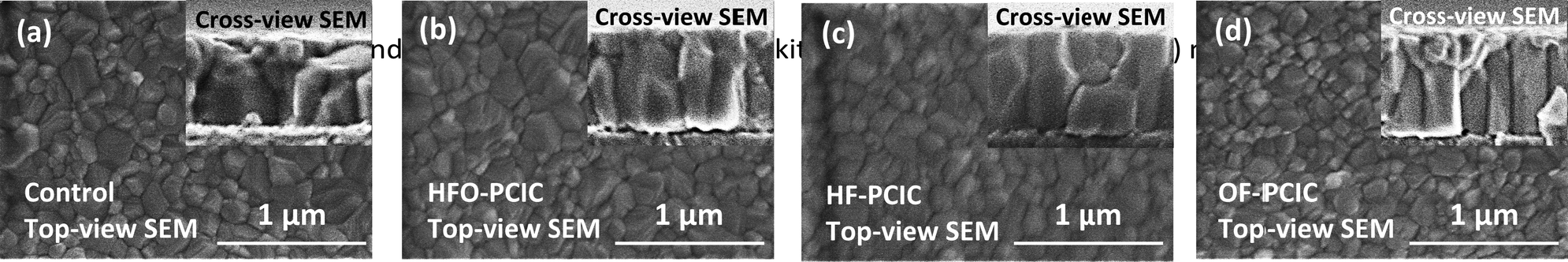
Considering that the morphology also affects the charge transport greatly, scanning electron microscopy (SEM) measurements were performed to investigate the morphology of the perovskite film. Fig. 3 shows the surface morphology of the perovskite films without and with different NFAs. All films have large grain sizes, and the surface structure has no significant change. These results exclude the possibility of morphology effect on the carrier mobility variation with different NFA additions.
 |
| | Fig. 3 SEM top-view images and cross-view images of perovskite active layers mixed with (a) none, (b) HFO-PCIC, (c) HF-PCIC, and (d) OF-PCIC. | |
For a PVSC device, the vertical charge transport plays a dominant role in determining the charge collection, rather than the lateral charge transport. Therefore, we have studied the cross-section morphology of the PVSCs. As shown in Fig. 3, all the perovskite films without or with different NFAs show large grains, which connect the electron transport layer (ETL) and hole transport layer (HTL). This means the inter-grain charge transport will not be a very severe issue for the PVSCs with optimized thickness, which is comparable with the grain size. On the other hand, the inter-grain charge transport might be the reason underlying the thickness limit of the optimal PVSCs.
PVSCs with a thick active layer
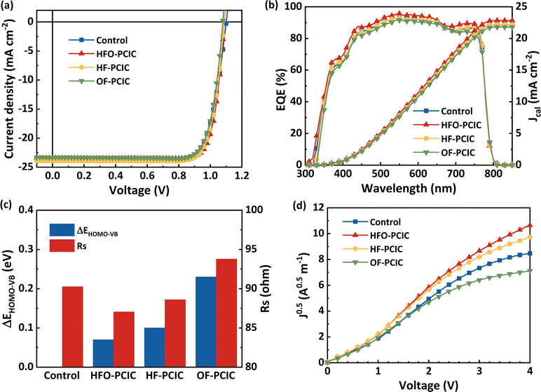
It is obvious that the inter-grain will become more and more important for the thicker film, because the number of grain boundaries increases significantly, with the increase of thickness.59 To amplify the role of NFAs on the device performance of PVSCs and take a further look into the effect of inter-grain energetic structure, it is necessary to create more vertical charge transporting “gaps” or grain boundaries. Therefore, PVSCs with a thick perovskite layer of over 1500 nm thick were fabricated. Fig. 4a shows the J–V characteristic curves of the PVSCs with a thick active layer (1500 nm), and their device parameters are summarized in Table 3. Fig. 4b shows PCE and Rs distribution statistics of the PVSCs with the perovskite layer over 1500 nm. As shown, after increasing the thickness of the perovskite active layer to 1500 nm, the device performance of the control PVSCs decreases rapidly, with the averaged efficiency dropping from 20.10% (700 nm) to 17.10% (1500 nm) and the best efficiency from 20.67% (700 nm) to 19.60% (1500 nm). For the PVSCs with HFO-PCIC modification, the device performance drop is significantly alleviated with the thickness increasing from 700 nm to 1500 nm. Specifically, with HFO-PCIC incorporation, the averaged efficiency of 1500 nm PVSCs shows an average efficiency of 19.19% and best efficiency of 20.75%, which are comparable to the control device (700 nm), 20.10% and 20.67%, respectively. The variation in device performance is in good agreement with that in Rs, as shown in Fig. 4b. The use of HFO-PCIC decreases the Rs of PVSCs with 1500 nm thickness. Similarly, the addition of OF-IPCIC increases the Rs and harms the device performance, as shown in Table S3 (ESI†). These results confirm the unique advantage of HFO-PCIC or the FBQW structure for improving the charge transport across the grain boundary, which enables good tolerance on the thickness for future commercialization with robust manufacturing.
 |
| | Fig. 4 (a) J–V characteristics. (b) PCE and Rs distribution statistics of the PVSCs with the perovskite layer over 1500 nm. (c) The diagrammatic sketch of the test process of the horizontal charge transport. (d) I–V characteristics of the PVSCs in a horizontal transmission test. | |
Table 3 Photovoltaic performances of PVSCs over 1500 nm under AM 1.5 G illumination (100 mW cm−2). The average values were obtained from 20 cells
| NFA |
ΔEHOMO-VB (eV) |
V
OC (V) |
J
SC (mA cm−2) |
FF (%) |
R
s (Ω cm−2) |
PCE (%) |
Horizontal carrier mobility (cm2 V−1 s−1) |
| None |
0 |
1.07 |
20.09 |
79.65 |
105.39 |
17.10 ± 1.54 |
0.18 |
| HFO-PCIC |
0.07 |
1.095 |
22.185 |
78.99 |
100.95 |
19.19 ± 1.12 |
1.03 |
Horizontal charge transport
Compared to the vertical charge transport, the charge carriers will have to cross a greater grain boundary “gap” when transporting laterally, and this provides a good platform to further test the efficacy of the NFAs or the grain boundary energetic structure on the charge transport properties of the perovskite film. Therefore, to further study the effect of inter-grain energetic structure on the charge transport behaviors, we have measured the horizontal charge transport of the perovskite film/device. The schematic diagram of the test method is shown in Fig. 4c, and the device structure involves glass/NiOx/PTAA/MAPbI3. The resistivity of perovskite film is measured at low bias voltage, where the low injection current will cause a very small disturbance on band structure variation. Therefore, in this region, the carrier mobility can be simply derived from the resistivity of the perovskite, using the following equations:| |  | (2) |
where ρ is the resistivity, R is the electrical resistance, S is the cross-sectional area of the tested perovskite (= 4.9 × 10⁻¹⁰ m2), L is the length of the charge transport along the tested perovskite (= 0.1 mm), σ is the electrical conductivity, e is the elementary charge (= 1.6 × 10⁻¹⁹ C), n is the carrier density (= 1015 cm−3),19 and μ is the carrier mobility. The I–V characteristic curves of the PVSCs without or with HFO-PCIC and OF-PCIC are shown in Fig. 4d. The MAPbI3 perovskite film without any NFAs exhibits mobility of 0.18 cm2 V−1 s−1. As listed in Table 3, by blending with the HFO-PCIC, which forms a low charge transporting barrier FBQW structure, the carrier mobility increases to 1.03 cm2 V−1 s−1. While with blending OF-PCIC, which forms a high charge transporting barrier, the carrier mobility decreases to 0.09 cm2 V−1 s−1. This result is consistent with the device performance and the SCLC results but is more explicit and amplified. Therefore, this result further confirms that the addition of suitable NFAs to form the FBQW structure could remedy the grain boundaries for smooth charge transport and high device performance with good thickness tolerance.
Discussion
The fundamentals of FBQW are based on the electron tunneling effect. At a spaced interface, the electron can directly hop over the gap when the distance is short. The electron tunneling current between the adjacent perovskite crystal is determined by both the distance and the energy offset, as conforms to the following equation:| |  | (3) |
where A is a constant, which is relevant to the nature of the materials, surrounding conditions, and the geometry of the quantum well, m is the electron mass, Φ is the barrier height, d is the barrier distance, ħ is Planck's constant, e is the electron charge, and V is the applied voltage. For the perovskite film, Φ is determined by the energy offset between the perovskite and the matters at the grain boundary, which might be excessive PbI2, MAI or vacancy before any modification at the grain boundary. Therefore, this Φ is expected to be very large. However, the use of NFAs with energy levels aligning with perovskite crystal will dramatically reduce the Φ, and thus, remedy the charge transport between the grain boundary significantly.
Experimental
Materials
All commercial materials were used as received without further purification. ITO glass (sheet resistance ≤ 10 Ω cm2) and methyl-ammonium iodide (MAI, 99%) were ordered from MaterWin. PbI2 (99%), PC61BM, (99.5%), PTAA (99%) and Spiro-MeOTAD were purchased from Xi’an Polymer Light Technology Corp. Ethylenediamine, ethylene glycol, N,N-dimethylformamide (DMF, 99%) and BCP (99%) were purchased from TCI. PEDOT:PSS aqueous solution (Al 4083) was purchased from Baytron. 1-Methyl-2-pyrrolidinone (NMP, 99.9%), toluene (99%), nickel nitrate (Ni (NO3)2·6H2O) and chlorobenzene (99%) were purchased from Aldrich. Ethanol was purchased from Aladdin. Silver (Ag, 99.99%) was purchased from commercial sources.
Device fabrication
ITO glass was washed successively in detergent, deionized water, acetone, isopropanol, and ethanol for 15 minutes, respectively. Then, the substrates were dried in an air oven at a temperature of 100 °C. After ITO glass was treated with ultraviolet ozone for 20 minutes, NiOx precursor solution (Ni(NO3)2·6H2O/ethylenediamine = 1/1 M/M) was spin-coated on ITO glass at 4000 rpm for 30 s, calcining at 120 °C and 315 °C for 30 minutes and 60 minutes, respectively. Then all the next steps were carried out in a glove box, where the moisture content was roughly equivalent to 0% (0.5![[thin space (1/6-em)]](https://www.rsc.org/images/entities/char_2009.gif) ppm). A thin layer of PTAA (1 mg mL−1 in toluene) was spin-coated onto NiOx substrate at 6000 rpm for 30 s, then transferred to a hot plate at 100 °C for annealing for 15 minutes. Before spin-coating, the perovskite active layer, the prepared substrate and perovskite precursor solution (1.2 M, MAI/PbI2 = 1/1 M/M in DMF/NMP = 4/1 v/v) were heated at 70 °C for 20 minutes. To prepare high-quality perovskite film, the substrate was quickly moved to the spin coater, then 60 μL hot precursor solution was dropped onto the substrate. The spin-coating process of perovskite includes two stages. In the first stage, the spinning speed is 1000 rpm, the coating time is 5 s, and the acceleration is 500 rpm s−1. In the second stage, the spinning speed is 6000 rpm, the coating time is 40 s, and the acceleration is 3000 rpm s−1. Importantly, 120 μL of toluene was added to the substrate after 4 s of the second stage of spin coating. Finally, the substrate was moved to a hot plate at 100 °C for annealing for 2 minutes. When the active layer has been prepared, PC61BM (15 mg mL−1 in chlorobenzene) and BCP (1 mg mL−1 in ethanol) was added to the substrate successively at 3000 rpm for 30 s, respectively. Finally, the finished samples were transferred to the evaporation chamber to deposit 100 nm Ag.
ppm). A thin layer of PTAA (1 mg mL−1 in toluene) was spin-coated onto NiOx substrate at 6000 rpm for 30 s, then transferred to a hot plate at 100 °C for annealing for 15 minutes. Before spin-coating, the perovskite active layer, the prepared substrate and perovskite precursor solution (1.2 M, MAI/PbI2 = 1/1 M/M in DMF/NMP = 4/1 v/v) were heated at 70 °C for 20 minutes. To prepare high-quality perovskite film, the substrate was quickly moved to the spin coater, then 60 μL hot precursor solution was dropped onto the substrate. The spin-coating process of perovskite includes two stages. In the first stage, the spinning speed is 1000 rpm, the coating time is 5 s, and the acceleration is 500 rpm s−1. In the second stage, the spinning speed is 6000 rpm, the coating time is 40 s, and the acceleration is 3000 rpm s−1. Importantly, 120 μL of toluene was added to the substrate after 4 s of the second stage of spin coating. Finally, the substrate was moved to a hot plate at 100 °C for annealing for 2 minutes. When the active layer has been prepared, PC61BM (15 mg mL−1 in chlorobenzene) and BCP (1 mg mL−1 in ethanol) was added to the substrate successively at 3000 rpm for 30 s, respectively. Finally, the finished samples were transferred to the evaporation chamber to deposit 100 nm Ag.
The fabrication process of over 1500 nm devices is consistent with the description above, but the concentration of perovskite precursor solution has changed to 2.0 M. The concentration of NFAs in perovskite precursor solution is the respective saturation concentration in DMF, and the relationship between the additive amount and the PCE is shown in Fig. S4 (ESI†).
For the horizontal charge transport test, the configuration of the PVSCs is glass/NiOx/PTAA/MAPbI3 and the preparation method of each layer is the same as that mentioned above.
Characterization
The J–V measurement was performed on the solar simulator (SS-X50, Enlitech) along with AM 1.5G spectra whose intensity was calibrated by the certified standard silicon solar cell (KG2, Enlitech) at 100 mW cm2. The mismatch value is between 0.997 and 1.003. The area of the device was defined as 0.05979 cm2 by the certified metal mask. EQE data were measured via the solar-cell spectral-response measurement system (QE-R, Enlitech). UV-vis absorption spectra were recorded on a Shimadzu UV-1800 spectrophotometer. SEM images were obtained from a Hitachi S-4800. The I–V curves in the horizontal charge transport were obtained by the semiconductor parameter analyzer (Keysight B1500A). PL and TRPL spectra were obtained using an FLSP920 spectrofluorometer at an excitation wavelength of 515 nm. The device for the stability test is stored in the N2 glove box without package.
Conclusions
To sum up, we modified the perovskite inter-grain energetic structure via an organic semiconductor and investigated the effects on the charge transport properties of perovskite film and the device performance of perovskite solar cells (PVSCs). In particular, we have proposed that a “flat band” quantum well structure (FBQW, where the HOMO and LUMO of the organic semiconductor are aligned with the VB and CB of the perovskite, respectively) can effectively improve the charge transport across grain boundaries, and results in a high device performance of over 21% for MAPbI3 PVSCs. Moreover, this strategy or concept breaks the thickness limit of the optimal device (similar to the grain boundary and less than 1000 nm) and enables good thickness tolerance. Therefore, with the FBQW energetic structure, the PVSCs with 1500 nm perovskite layer exhibit the best efficiency of 20.75%, which is among the best for thick film PVSCs. The effects of inter-grain energetic structure on the charge transport of perovskite film and the efficacy of the FBQW are further studied and confirmed via the space-charge-limited-current measurement, and these effects are amplified with the horizontal charge transport device structure. Therefore, our work proposes a novel concept/strategy of FBQW structure to remedy the inter-grain charge transport and enables good thickness tolerance for future commercialization of PVSCs.
Author contributions
L. Z. conceived the idea and proposed the concept of a FBQW structure. L. Z. and Y. C. designed the experiments. Y. C. completed the device fabrication. Y. C., F. W., C. X. and H. W. contributed to the result analysis. S. L. synthesized the HFO-PCIC, HF-PCIC and OF-PCIC. T. C. performed morphology characterization. X. W., B. P. and H. L. performed the horizontal charge transport measurements. Y. C. and L. Z. prepared the manuscript. L.Z. and H.C. supervised this work. All authors commented on the manuscript.
Conflicts of interest
There are no conflicts to declare.
Acknowledgements
This work was supported by the Fundamental Research Funds for the Central Universities (No. 226-2022-00133 and No. 226-2022-00209), the “Pioneering” and “Leading Goose” R&D Program of Zhejiang (2022C01104), the research start up fund from Zhejiang University, and the National Natural Science Foundation of China (No. 52127806, 52173185, 21734008, and 61721005).
Notes and references
- Q. Dong, Y. Fang, Y. Shao, P. Mulligan, J. Qiu, L. Cao and J. Huang, Electron-hole diffusion lengths >175 um in solution-grown CH3NH3PbI3 single crystals, Science, 2015, 347, 967–970 CrossRef CAS PubMed.
- D. W. deQuilettes, S. M. Vorpahl, S. D. Stranks, H. Nagaoka, G. E. Eperon, M. E. Ziffer, H. J. Snaith and D. S. Ginger, Impact of microstructure on local carrier lifetime in perovskite solar cells, Science, 2015, 348, 683–686 CrossRef CAS PubMed.
- S. D. Stranks, G. E. Eperon, G. Grancini, C. Menelaou, M. J. P. Alcocer, T. Leijtens, L. M. Herz, A. Petrozza and H. J. Snaith, Electron-Hole Diffusion Lengths Exceeding 1 Micrometer in an Organometal Trihalide Perovskite Absorber, Science, 2013, 342, 341–344 CrossRef CAS PubMed.
- B. Yan, X. Liu, W. Lu, M. Feng, H. Yan, Z. Li, S. Liu, C. Wang, J. Hu and D. Xue, Indoor photovoltaics awaken the world’s first solar cells, Sci. Adv., 2022, 8, eadc9923 CrossRef CAS PubMed.
- Y. Jiang, C. Sun, J. Xu, S. Li, M. Cui, X. Fu, Y. Liu, Y. Liu, H. Wan, K. Wei, T. Zhou, W. Zhang, Y. Yang, J. Yang, C. Qin, S. Gao, J. Pan, Y. Liu, S. Hoogland, E. H. Sargent, J. Chen and M. Yuan, Synthesis-on-substrate of quantum dot solids, Nature, 2022, 612, 679–684 CrossRef CAS PubMed.
- L. Zuo, X. Shi, W. Fu and A. K. Jen, Highly Efficient Semitransparent Solar Cells with Selective Absorption and Tandem Architecture, Adv. Mater., 2019, 31, 1901683 CrossRef PubMed.
- Z. Li, B. Li, X. Wu, S. A. Sheppard, S. Zhang, D. Gao, N. J. Long and Z. Zhu, Organometallic-functionalized interfaces for highly efficient inverted perovskite solar cells, Science, 2022, 376, 416–420 CrossRef CAS PubMed.
- R. He, S. Ren, C. Chen, Z. Yi, Y. Luo, H. Lai, W. Wang, G. Zeng, X. Hao, Y. Wang, J. Zhang, C. Wang, L. Wu, F. Fu and D. Zhao, Wide-bandgap organic–inorganic hybrid and all-inorganic perovskite solar cells and their application in all-perovskite tandem solar cells, Energy Environ. Sci., 2021, 14, 5723–5759 RSC.
- C. H. Liao, C. H. Chen, J. Bing, C. Bailey, Y. T. Lin, T. M. Pandit, L. Granados, J. Zheng, S. Tang, B. H. Lin, H. W. Yen, D. R. McCamey, B. J. Kennedy, C. C. Chueh and A. W. Y. Ho-Baillie, Inorganic-Cation Pseudohalide 2D Cs2Pb(SCN)2Br2 Perovskite Single Crystal, Adv. Mater., 2022, 34, 2104782 CrossRef CAS PubMed.
- H. Wang, X. Gong, D. Zhao, Y.-B. Zhao, S. Wang, J. Zhang, L. Kong, B. Wei, R. Quintero-Bermudez, O. Voznyy, Y. Shang, Z. Ning, Y. Yan, E. H. Sargent and X. Yang, A Multi-functional Molecular Modifier Enabling Efficient Large-Area Perovskite Light-Emitting Diodes, Joule, 2020, 4, 1977–1987 CrossRef CAS.
- A. Kojima, K. Teshima, Y. Shirai and T. Miyasaka, Organometal Halide Perovskites
as Visible-Light Sensitizers for Photovoltaic Cells, J. Am. Chem. Soc., 2009, 131, 6050–6051 CrossRef CAS PubMed.
- X. Wu, B. Li, Z. Zhu, C. C. Chueh and A. K.-Y. Jen, Designs from single junctions, heterojunctions to multijunctions for high-performance perovskite solar cells, Chem. Soc. Rev., 2021, 50, 13090–13128 RSC.
- X. Wu, Y. Liu, F. Qi, F. Lin, H. Fu, K. Jiang, S. Wu, L. Bi, D. Wang, F. Xu, A. K.-Y. Jen and Z. Zhu, Improved stability and efficiency of perovskite/organic tandem solar cells with an all-inorganic perovskite layer, J. Mater. Chem. A, 2021, 9, 19778–19787 RSC.
- M. G. Mohamed, C.-C. Lee, A. F. M. EL-Mahdy, J. Lüder, M.-H. Yu, Z. Li, Z. Zhu, C.-C. Chueh and S.-W. Kuo, Exploitation of two-dimensional conjugated covalent organic frameworks based on tetraphenylethylene with bicarbazole and pyrene units and applications in perovskite solar cells, J. Mater. Chem. A, 2020, 8, 11448–11459 RSC.
- X. Li, X. Wu, B. Li, Z. Cen, Y. Shang, W. Lian, R. Cao, L. Jia, Z. Li, D. Gao, X. Jiang, T. Chen, Y. Lu, Z. Zhu and S. Yang, Modulating the deep-level defects and charge extraction for efficient perovskite solar cells with high fill factor over 86%, Energy Environ. Sci., 2022, 15, 4813–4822 RSC.
- M.-H. Yu, P.-C. Han, C.-C. Lee, I.-C. Ni, Z. Zhu, E. Z. Kurmaev, S. Furukawa, K. C.-W. Wu and C.-C. Chueh, A self-arranged metal–organic polyhedron/fullerene asymmetric structure improves the performance of inverted perovskite solar cells, J. Mater. Chem. C, 2022, 10, 14542–14548 RSC.
- S. Shan, C. Xu, H. Wu, B. Niu, W. Fu, L. Zuo and H. Chen, Manipulating the Crystallization and Phase Transition for High-Performance CsPbI2Br Solar Cells, Adv. Energy Mater., 2023, 13, 2203682 CrossRef CAS.
- S. Shan, Y. Li, H. Wu, T. Chen, B. Niu, Y. Zhang, D. Wang, C. Kan, X. Yu, L. Zuo and H. Chen, Manipulating the film morphology evolution toward green solvent-processed perovskite solar cells, SusMat, 2021, 1, 537–544 CrossRef CAS.
- Z. Ni, C. Bao, Y. Liu, Q. Jiang, W. Wu, S. Chen, X. Dai, B. Chen, B. Hartweg, Z. Yu, Z. Holman and J. Huang, Resolving spatial and energetic distributions of trap states in metal halide perovskite solar cells, Science, 2020, 367, 1352–1358 CrossRef CAS PubMed.
- N. J. Jeon, J. H. Noh, W. S. Yang, Y. C. Kim, S. Ryu, J. Seo and S. I. Seok, Compositional engineering of perovskite materials for high-performance solar cells, Nature, 2015, 517, 476–480 CrossRef CAS PubMed.
- N. J. Jeon, J. H. Noh, Y. C. Kim, W. S. Yang, S. Ryu and S. I. Seok, Solvent engineering for high-performance inorganic-organic hybrid perovskite solar cells, Nat. Mater., 2014, 13, 897–903 CrossRef CAS PubMed.
- N. G. Park, Methodologies for high efficiency perovskite solar cells, Nano Convergence, 2016, 3, 15 CrossRef PubMed.
- H. Zhou, Q. Chen, G. Li, S. Luo, T. Song, H. Duan, Z. Hong, J. You, Y. Liu and Y. Yang, Interface engineering of highly efficient perovskite solar cells, Science, 2014, 345, 542–546 CrossRef CAS PubMed.
- M. Liu, M. B. Johnston and H. J. Snaith, Efficient planar heterojunction perovskite solar cells by vapour deposition, Nature, 2013, 501, 395–398 CrossRef CAS PubMed.
- F. Wu, K. Yan, H. Wu, B. Niu, Z. Liu, Y. Li, L. Zuo and H. Chen, Tuning interfacial chemical interaction for high-performance perovskite solar cell with PEDOT:PSS as hole transporting layer, J. Mater. Chem. A, 2021, 9, 14920–14927 RSC.
- C. Xu, L. Zuo, P. Hang, X. Guo, Y. Pan, G. Zhou, T. Chen, B. Niu, X. Xu, Z. Hong, D. Wang, H. Zhu, X. Yu, D. Yang and H. Chen, Synergistic effects of bithiophene ammonium salt for high-performance perovskite solar cells, J. Mater. Chem. A, 2022, 10, 9971–9980 RSC.
- B. Niu, H. Wu, J. Yin, B. Wang, G. Wu, X. Kong, B. Yan, J. Yao, C.-Z. Li and H. Chen, Mitigating the Lead Leakage of High-Performance Perovskite Solar Cells via In Situ Polymerized Networks, ACS Energy Lett., 2021, 6, 3443–3449 CrossRef CAS.
- L. Zuo, Z. Gu, T. Ye, W. Fu, G. Wu, H. Li and H. Chen, Enhanced photovoltaic performance of CH3NH3PbI3 perovskite solar cells through interfacial engineering using self-assembling monolayer, J. Am. Chem. Soc., 2015, 137, 2674–2679 CrossRef CAS PubMed.
- L. Zuo, Q. Chen, N. De Marco, Y. T. Hsieh, H. Chen, P. Sun, S. Y. Chang, H. Zhao, S. Dong and Y. Yang, Tailoring the Interfacial Chemical Interaction for High-Efficiency Perovskite Solar Cells, Nano Lett., 2017, 17, 269–275 CrossRef CAS PubMed.
- F. Wu, K. Yan, H. Wu, Y. Guo, S. Shan, T. Chen, W. Fu, L. Zuo and H. Chen, Polypropylene Glycol-Modified Anode Interface for High-Performance Perovskite Solar Cells, Chin. J. Chem., 2022, 40, 2694–2700 CrossRef CAS.
- L. He, H. Wu, X. Lian, L. Zuo, G. Wu and H. Chen, Efficient and stable inverted perovskite solar cells incorporating 4-Fluorobenzylammonium iodide, Org. Electron., 2021, 92, 106124 CrossRef CAS.
- F. U. Kosasih, E. Erdenebileg, N. Mathews, S. G. Mhaisalkar and A. Bruno, Thermal evaporation and hybrid deposition of perovskite solar cells and mini-modules, Joule, 2022, 6, 2692–2734 CrossRef CAS.
- Q. Jiang, J. Tong, R. A. Scheidt, X. Wang, A. E. Louks, Y. Xian, R. Tirawat, A. F. Palmstrom, M. P. Hautzinger, S. P. Harvey, S. Johnston, L. T. Schelhas, B. W. Larson, E. L. Warren, M. C. Beard, J. J. Berry, Y. Yan and K. Zhu, Compositional texture engineering for highly stable wide-bandgap perovskite solar cells, Science, 2022, 378, 1295–1300 CrossRef CAS PubMed.
- Q. Cheng, H. Chen, F. Yang, Z. Chen, W. Chen, H. Yang, Y. Shen, X. M. Ou, Y. Wu, Y. Li and Y. Li, Molecular Self-Assembly Regulated Dopant-Free Hole Transport Materials for Efficient and Stable n-i-p Perovskite Solar Cells and Scalable Modules, Angew. Chem., Int. Ed., 2022, 61, 202210613 Search PubMed.
- F. Huang, Y. Dkhissi, W. Huang, M. Xiao, I. Benesperi, S. Rubanov, Y. Zhu, X. Lin, L. Jiang, Y. Zhou, A. Gray-Weale, J. Etheridge, C. R. McNeill, R. A. Caruso, U. Bach, L. Spiccia and Y.-B. Cheng, Gas-assisted preparation of lead iodide perovskite films consisting of a monolayer of single crystalline grains for high efficiency planar solar cells, Nano Energy, 2014, 10, 10–18 CrossRef CAS.
- H. S. Kim and N. G. Park, Parameters Affecting I-V Hysteresis of CH3NH3PbI3 Perovskite Solar Cells: Effects of Perovskite Crystal Size and Mesoporous TiO2 Layer, J. Phys. Chem. Lett., 2014, 5, 2927–2934 CrossRef CAS PubMed.
- J. Jeong, M. Kim, J. Seo, H. Lu, P. Ahlawat, A. Mishra, Y. Yang, M. A. Hope, F. T. Eickemeyer, M. Kim, Y. J. Yoon, I. W. Choi, B. P. Darwich, S. J. Choi, Y. Jo, J. H. Lee, B. Walker, S. M. Zakeeruddin, L. Emsley, U. Rothlisberger, A. Hagfeldt, D. S. Kim, M. Gratzel and J. Y. Kim, Pseudo-halide anion engineering for alpha-FAPbI3 perovskite solar cells, Nature, 2021, 592, 381–385 CrossRef CAS PubMed.
- J. Li, L. Zuo, H. Wu, B. Niu, S. Shan, G. Wu and H. Chen, Universal Bottom Contact Modification with Diverse 2D Spacers for High-Performance Inverted Perovskite Solar Cells, Adv. Funct. Mater., 2021, 31, 2104036 CrossRef CAS.
- L. Duan and A. Uddin, Defects and stability of perovskite solar cells: a critical analysis, Mater. Chem. Front., 2022, 6, 400–417 RSC.
- A. R. b Mohd Yusoff, M. Vasilopoulou, D. G. Georgiadou, L. C. Palilis, A. Abate and M. K. Nazeeruddin, Passivation and process engineering approaches of halide perovskite films for high efficiency and stability perovskite solar cells, Energy Environ. Sci., 2021, 14, 2906–2953 RSC.
- T. Wu, Y. Wang, X. Li, Y. Wu, X. Meng, D. Cui, X. Yang and L. Han, Efficient Defect Passivation for Perovskite Solar Cells by Controlling the Electron Density Distribution of Donor-π-Acceptor Molecules, Adv. Energy Mater., 2019, 9, 1803766 CrossRef.
- T. H. Han, J. W. Lee, C. Choi, S. Tan, C. Lee, Y. Zhao, Z. Dai, N. De Marco, S. J. Lee, S. H. Bae, Y. Yuan, H. M. Lee, Y. Huang and Y. Yang, Perovskite-polymer composite cross-linker approach for highly-stable and efficient perovskite solar cells, Nat. Commun., 2019, 10, 520 CrossRef CAS PubMed.
- X. Lian, H. Wu, L. Zuo, G. Zhou, X. Wen, Y. Zhang, G. Wu, Z. Xie, H. Zhu and H. Chen, Stable Quasi-2D Perovskite Solar Cells with Efficiency over 18% Enabled by Heat–Light Co-Treatment, Adv. Funct. Mater., 2020, 30, 2004188 CrossRef CAS.
- H. Wu, X. Lian, S. Tian, Y. Zhang, M. Qin, Y. Zhang, F. Wang, X. Lu, G. Wu and H. Chen, Additive-Assisted Hot-Casting Free Fabrication of Dion–Jacobson 2D Perovskite Solar Cell with Efficiency Beyond 16%, Sol. RRL, 2020, 4, 2000087 CrossRef CAS.
- L. Zuo, H. Guo, D. W. deQuilettes, S. Jariwala, N. De Marco, S. Dong, R. DeBlock, D. S. Ginger, B. Dunn, M. Wang and Y. Yang, Polymer-modified halide perovskite films for efficient and stable planar heterojunction solar cells, Sci. Adv., 2017, 3, 1700106 CrossRef PubMed.
- Y. Huang, K. Yan, B. Niu, Z. Chen, E. Gu, H. Liu, B. Yan, J. Yao, H. Zhu, H. Chen and C.-Z. Li, Finite perovskite hierarchical structures via ligand confinement leading to efficient inverted perovskite solar cells, Energy Environ. Sci., 2023, 16, 557–564 RSC.
- R. Qiao and L. Zuo, Self-assembly monolayers boosting organic–inorganic halide perovskite solar cell performance, J. Mater. Res., 2018, 33, 387–400 CrossRef CAS.
- Y. Guo, H. Wu, Z. Liu, S. Shan, B. Niu, X. Lian, L. Zuo and H. Chen, Manipulating Perovskite Precursor Solidification toward 21% Pristine MAPbI3 Solar Cells, Sol. RRL, 2021, 5, 2100114 CrossRef CAS.
- L. Zuo, S. Dong, N. De Marco, Y. T. Hsieh, S. H. Bae, P. Sun and Y. Yang, Morphology Evolution of High Efficiency Perovskite Solar Cells via Vapor Induced Intermediate Phases, J. Am. Chem. Soc., 2016, 138, 15710–15716 CrossRef CAS PubMed.
- M. C. López-González, G. del Pozo, D. Martín-Martín, L. Muñoz-Díaz, J. C. Pérez-Martínez, E. Hernández-Balaguera, B. Arredondo, Y. Galagan, M. Najafi and B. Romero, Evaluation of Active Layer Thickness Influence in Long-Term Stability and Degradation Mechanisms in CsFAPbIBr Perovskite Solar Cells, Appl. Sci., 2021, 11, 11668 CrossRef.
- J. Yang, E. L. Lim, L. Tan and Z. Wei, Ink Engineering in Blade-Coating Large-Area Perovskite Solar Cells, Adv. Energy Mater., 2022, 12, 2200975 CrossRef CAS.
- Y. Yu, J. Li, D. Geng, J. Wang, L. Zhang, T. L. Andrew, M. S. Arnold and X. Wang, Development of Lead Iodide Perovskite Solar Cells Using Three-Dimensional Titanium Dioxide Nanowire Architectures, ACS Nano, 2015, 9, 564–572 CrossRef CAS PubMed.
- W. Fu, T. Zhao, H. Liu, F. Lin, L. Zuo, X. Li and A. K. Y. Jen, High-Efficiency Quasi-2D Perovskite Solar Cells Incorporating 2,2′-Biimidazolium Cation, Sol. RRL, 2021, 5, 2000700 CrossRef CAS.
- Z. Zhang, M. Sheri, Z. A. Page, T. Emrick, A. Saeki, Y. Liu and T. P. Russell, Understanding Hole Extraction of Inverted Perovskite Solar Cells, ACS Appl. Mater. Interfaces, 2020, 12, 56068–56075 CrossRef CAS PubMed.
- L. Zuo, Z. Li and H. Chen, Ion migration and accumulation in halide perovskite solar cells, Chin. J. Chem., 2022, 41, 861–876 CrossRef.
- W. Cha, W.-Y. Cha, I. Noh, S. Seki, H. Ohkita and D. Kim, Controlling the charge carrier dynamics by modulating the orientation diversity of perovskites, Mater. Chem. Front., 2022, 6, 1026–1032 RSC.
- S. Li, L. Zhan, W. Zhao, S. Zhang, B. Ali, Z. Fu, T.-K. Lau, X. Lu, M. Shi, C.-Z. Li, J. Hou and H. Chen, Revealing the effects of molecular packing on the performances of polymer solar cells based on A–D–C–D–A type non-fullerene acceptors, J. Mater. Chem. A, 2018, 6, 12132–12141 RSC.
- S. S. Shin, S. J. Lee and S. I. Seok, Exploring wide bandgap metal oxides for perovskite solar cells, APL Mater., 2019, 7, 022401 CrossRef.
- J. Chen, L. Zuo, Y. Zhang, X. Lian, W. Fu, J. Yan, J. Li, G. Wu, C.-Z. Li and H. Chen, High-Performance Thickness Insensitive Perovskite Solar Cells with Enhanced Moisture Stability, Adv. Energy Mater., 2018, 8, 1800438 CrossRef.
|
| This journal is © the Partner Organisations 2023 |
Click here to see how this site uses Cookies. View our privacy policy here. 
 ab,
Fei
Wu
a,
Chang
Xu
a,
Haotian
Wu
a,
Shuixing
Li
a,
Xinru
Wang
a,
Tianyi
Chen
a,
Boyu
Peng
ab,
Fei
Wu
a,
Chang
Xu
a,
Haotian
Wu
a,
Shuixing
Li
a,
Xinru
Wang
a,
Tianyi
Chen
a,
Boyu
Peng