
Understanding the synergistic influence of the propylammonium bromide additive and erbium-doped CsPbI2Br for highly stable inorganic perovskite solar cells†
Jyoti V.
Patil
ab,
Sawanta S.
Mali
 b,
Shivaji B.
Sadale
c and
Chang Kook
Hong
*ab
b,
Shivaji B.
Sadale
c and
Chang Kook
Hong
*ab
aOptoelectronic Convergence Research Center, School of Chemical Engineering, Chonnam National University, Gwangju, South Korea 61186. E-mail: hongck@chonnam.ac.kr
bPolymer Energy Materials Laboratory, School of Chemical Engineering, Chonnam National University, Gwangju, South Korea 61186
cEngineering Physics Laboratory, Department of Technology, Shivaji University, Kolhapur, Maharashtra 416004, India
First published on 23rd March 2023
Abstract
Inorganic cesium lead halide perovskites have gained increasing attention to boost photovoltaic performance and device stability. Nevertheless, the photoactive to photo-inactive phase transition under ambient conditions hampers its further enhancement. Here, we varied various amounts of propylammonium bromide (PABr) additive in the CsPbI2Br perovskite and further varied the erbium (ErCl3)-doped CsPbI2Br (herein CsPb1−nErnI2BrXn) (where X = Cl; 0 ≤ n < 1) perovskite. Further, in the optimized (CsPb0.97Er0.03I2BrCl0.09) composition, we studied the influence of various amounts of the PABr additive. Our results clearly show the PABr additive added film results in high-quality surface morphology, high crystallinity, and decreased trap-state density. Accordingly, our champion CsPb0.97Er0.03I2BrCl0.09 + 2 mg ml−1 PABr (CsEr-PA)-based inorganic perovskite solar cell (IPVSC) device showed 16.74% power conversion efficiency (PCE), which is much higher than that of bare (13.20%) and CsPb0.97Er0.03I2BrCl0.09-based perovskite devices (15.73%). In addition, the CsEr-PA-based IPVSC device revealed increased long-term stability, which maintained 90% of its initial PCE at 65 °C and thermal stress of over 400 h under ambient conditions. These dual stabilization strategies cover a new way to increase the photovoltaic performance of IPVSCs.
1. Introduction
Recently, the progress in inorganic perovskite solar cells (IPVSCs) has attracted increasing attention due to solving the poor thermal stability issue of the organic–inorganic hybrid perovskite solar cells (PVSCs).1 Due to the simple and air-processing ability, CsPbI3,2 CsPbBr3![[thin space (1/6-em)]](https://www.rsc.org/images/entities/char_2009.gif) 3 and CsPbI2Br4–8 perovskite compositions are popular in IPVSCs. Among the above-mentioned inorganic perovskite materials, CsPbI3 has a suitable band gap (∼1.7 eV) and it showed the highest 20.37% power conversion efficiency (PCE).9 Unfortunately, due to their unstable behavior and rapid phase transformation from the black CsPbI3 perovskite to yellow non-perovskite δ-phase at room temperature, it is difficult to maintain stable performance over a long period.10 Although, CsPbBr3 is a well-known material for long-term stability it produces a limited PCE of ∼10% because of the wide bandgap of 2.3 eV.11 Particularly, the CsPbI2Br perovskite material has become a very promising candidate for increasing PCE and stability of IPVSCs because the appropriate band gap of 1.92 eV.12 Thus, it is important to implement a new approach to cultivate more efficient and stable perovskite device performance.
3 and CsPbI2Br4–8 perovskite compositions are popular in IPVSCs. Among the above-mentioned inorganic perovskite materials, CsPbI3 has a suitable band gap (∼1.7 eV) and it showed the highest 20.37% power conversion efficiency (PCE).9 Unfortunately, due to their unstable behavior and rapid phase transformation from the black CsPbI3 perovskite to yellow non-perovskite δ-phase at room temperature, it is difficult to maintain stable performance over a long period.10 Although, CsPbBr3 is a well-known material for long-term stability it produces a limited PCE of ∼10% because of the wide bandgap of 2.3 eV.11 Particularly, the CsPbI2Br perovskite material has become a very promising candidate for increasing PCE and stability of IPVSCs because the appropriate band gap of 1.92 eV.12 Thus, it is important to implement a new approach to cultivate more efficient and stable perovskite device performance.
So far, various efforts have been made in order to stabilize the perovskite phase under ambient conditions and improve the device performance of the CsPbI2Br-based IPVSCs.13–18 For example, various metal ion doping at the A-site12–15 or B-site16–22 would facilitate suitable Goldschmidt's tolerance factor towards ideality, which can stabilize the phase of the perovskite material.23 According to the previous reports, doping and ion substitution represent an effective way to tailor the optical and electronic properties of the halide perovskites.16–25 In particular, rare earth ions, exhibit exceptional optical properties of sharp line spectra, tunable wavelengths, long lifetime, and large Stokes shifts because of their exceptional 4f electronic structure.26–29 In recent years, numerous studies have demonstrated the various rare-earth ions doped in the inorganic perovskite material. For example, Duan et al. reported partial substitution of Pb2+ with lanthanide series (Ln3+ = Sm3+, Tb3+, Ho3+, Er3+, and Yb3+) in the inorganic CsPbBr3-based IPVSCs with 10.14% PCE.27 Similarly, Pan et al., successfully doped a series of lanthanide ions into the CsPbCl3 perovskite, which showed that the rare-earth ions substituted the Pb2+ sites, which is easier to replace the Pb2+ site because of their suitable ionic radii. In addition, the doping of lanthanide ions shows tunable multi-colored emissions of visible to near-infrared regions and increased photoluminescence quantum yield.24 However, the combination of lead halide perovskite and rare-earth ions can give unique characteristics, such as high-quality films, decreased trap states, increased stability of perovskite, expanded absorption range, and as a result increased device performance.29–32 Likewise, rare-earth ions are doped in the organic–inorganic halide perovskite, which is comprehensively employed in photovoltaics.33–37 The main benefits of rare-earth ion doping involve a long lifetime, narrow emission wavelength, and high photochemical stability, and it can achieve a UV/Visible emission upon near-infrared excitation by the upconversion process.38 Usually, rare earth ions occur in the trivalent form, which is the most stable valence and is considered an upconversion luminescent material. These rare earth ion-doped upconversion materials (Yb3+, Tm3+, and Er3+) have attracted increasing attention due to their unique luminescent properties including high color purity, narrow spectrum, wide emission region, high transition efficiency, and long lifetime. Nevertheless, in the visible and infrared region, the electronic transition is the special f–f transition called a transition within the 4fn configuration of rare earth ions, generating noteworthy spectral properties.38,39 The trivalent rare earth (upconversion material) Er3+ is generally used as a sensitizer due to its abundant energy level and high energy absorption.38 Inspired by the above work, it is worthy to study the influence of Er3+ doping in the hot-air processed CsPbI2Br-based perovskite and its photovoltaic device performance.
Besides, organic additives in the perovskite precursor solution can control its crystallization growth rate, which results in high-quality perovskite thin films. This additive-assisted perovskite thin film synthesis can modify crystal growth and reduce grain boundary defects. So, for various kinds of additives such as formamidinium chloride (FACl),40 guanidinium iodide (GAI),41 ethylammonium bromide (EABr),42 butylammonium iodide (BAI),43 methylammonium bromide (MABr),44 formamidinium bromide (FABr),45 and methylammonium iodide (MAI)46 have been employed to control and or passivate the perovskite film surface. The above-mentioned additives can facilitate the hydrophobic surface, decrease the trap density and reduce interfacial recombination in the perovskite surface, enabling the improvement of the carrier lifetime and open-circuit voltage.47–49 In addition, it helps increase the properties of the perovskite film through the high grains and perovskite film coverage by retarding the crystallization process.50–52 Here, we emphasized the effect of additives and rare earth ions on the CsPbI2Br perovskite with the morphology, crystallization, and stability of perovskite devices and studied its photovoltaic performance in ambient conditions.
In this work, we used the propylammonium bromide (PABr) additive in the CsPbI2Br and erbium (Er3+) dopant in the CsPb1−nErnI2BrXn (X = Br or Cl; 0 ≤ n < 1) perovskite to increase the perovskite film quality, device performance, and its stability. It was observed that the PABr additive contributed to retard the crystallization process, which yielded micrometer-sized grains. The increased grain size, improved crystallinity, and reduced trap density were observed for the CsPbI2Br perovskite films by the synergistic influence of Er3+ doping and the PABr additive. Accordingly, the highest PCE of 16.74% was achieved for the CsEr-PA (CsPb0.97Er0.03I2BrCl0.09 − 2 mg ml−1 PABr) perovskite-based IPVSC device.
2. Results and discussion
To check the synergistic effect of the PABr additive and Er3+ doping, the PABr additive was first added to the CsPbI2Br-based solution. Here, we added different amounts of the PABr additive in the CsPbI2Br perovskite to check the effect on surface morphology. Further, to examine the role of Er3+ doping in the CsPbI2Br perovskite, the ErCl3 doping amounts with an Er/Pb molar ratio of 0 to 4% (CsPb0.99Er0.01I2BrCl0.03, CsPb0.98Er0.02I2BrCl0.06, CsPb0.97Er0.03I2BrCl0.09 and CsPb0.96Er0.04I2BrCl0.12 perovskite films) were doped in the CsPbI2Br precursors solution and deposited by the spin coating (please check the Experimental section). During the spin coating of perovskite films, we applied hot air flow (Fig. S1(a)†) to deposit high-quality films. Furthermore, in the optimized 3% Er3+-doped CsPbI2Br (CsPb0.97Er0.03I2BrCl0.09) perovskite film, we added different amounts of the PABr additive (1 to 4 mg ml−1). Details of the inorganic CsPbI2Br (Cs), CsPb0.97Er0.03I2BrCl0.09 (CsEr), and CsPb0.97Er0.03I2BrCl0.09 − 2 mg ml−1 PABr (CsEr-PA)-based thin films are described in the Experimental section. Fig. S1(b)† shows the time-dependent photographs of the retarded crystal growth. To check the effect of Er3+ doping and PABr additive in the CsPbI2Br perovskite morphology, we recorded scanning electron microscopy (SEM) images. Fig. 1(a–c) shows top-view SEM images of the Cs, CsEr, and CsEr-PA perovskite thin films and Fig. 1(d–f) reveals a cross-sectional view of the corresponding perovskite films based devices. The Cs-based film showed a rough surface, as shown in Fig. 1(a) and Fig. S2(a).† Fig. S2(b–d)† shows the SEM images of the PABr additive-added perovskite films s CsPbI2Br, Cs-1 mg ml−1 PABr, Cs-2 mg ml−1 PABr, and Cs-3 mg ml−1 PABr, respectively. Amongst the above perovskite samples, the Cs-2 mg ml−1 PABr-based film exhibited uniform, dense with an increased 900 nm grain size than the rest of the samples. Notably, the PABr additive is advantageous to improve the quality of the perovskite film. Fig. S3(a–d)† shows the SEM images of the CsPb0.99Er0.01I2BrCl0.03, CsPb0.98Er0.02I2BrCl0.06, CsPb0.97Er0.03I2BrCl0.09, and CsPb0.96Er0.04I2BrCl0.12 perovskite thin films. Among these films, the CsPb0.97Er0.03I2BrCl0.09-based film showed a smooth surface with uniform and pinhole-free morphology (Fig. 1(b) and Fig. S3(c)).† Furthermore, in this CsEr (CsPb0.97Er0.03I2BrCl0.09) optimized film, we added various amounts of PABr additives from 1 to 4 mg ml−1, Fig. S4(a–d).† The CsEr perovskite film was converted into uniform and compact morphology with enlarged grains and decreased grain boundaries through the PABr additive. Particularly, the CsEr-PA (CsPb0.97Er0.03I2BrCl0.09 − 2 mg ml−1 PABr) displayed the highest grain size of 1.6 μm, demonstrating that the proper addition of the PABr additive is advantageous to obtain high-quality perovskite films, Fig. 1(c) and Fig. S4(b).† The cross-sectional SEM images of the perovskite devices fabricated with different device configurations (Au/P3HT/perovskite/mp-TiO2/c-TiO2/FTO/glass) are shown in (Fig. 1(d–f)) and Fig. S2(e).† It is noteworthy that, the CsEr-PA (Fig. 1(f)) perovskite device shows a highly uniform and compact nature with a better film thickness than Cs (Fig. 1(d) Cs-PA Fig. S2(e)† and CsEr (Fig. 1(e))-based perovskite devices.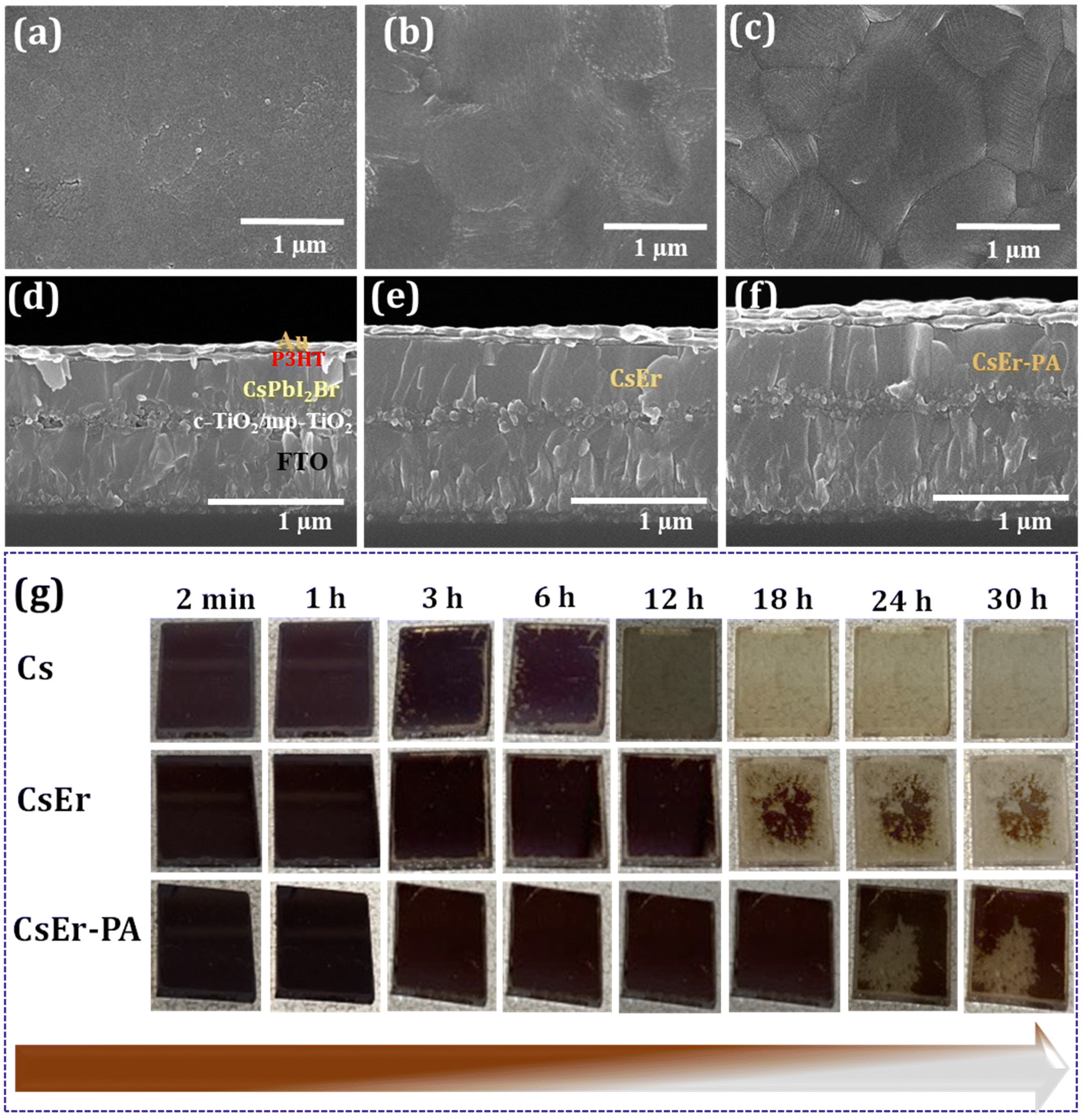 | ||
| Fig. 1 SEM top view images. (a) CsPbI2Br (Cs), (b) CsPb0.97Er0.03I2BrCl0.09 (CsEr), (c) CsPb0.97Er0.03I2BrCl0.09 + PABr-2 mg ml−1 (CsEr-PA) perovskite thin films. SEM cross-sectional view of (d) Cs, (e) CsEr, (f) CsEr-PA-based whole IPVSC devices and (g) different time exposure dependent photographic images of the Cs, CsEr and CsEr-PA perovskite thin films (Corresponding devices stored in ambient conditions at ∼25% RH without encapsulation). | ||
This will probably increase the charge carrier transport and decrease the charge recombination, which can facilitate improving the device's performance. Furthermore, we checked the phase stability of the Cs, CsEr, and CsEr-PA-based perovskite thin films under ambient conditions, as shown in Fig. 1(g). Remarkably, the initial photoactive black phase transition into the yellow phase was observed after 3 h for the Cs-based film, which is quite faster than that for the CsEr-based perovskite film (12 h). Nonetheless, no visible phase transition signs were observed up to 22 h for the CsEr-PA-based perovskite film, which is attributed to increased phase stability. This increment of structural stability is attributed to the contraction of the perovskite crystal brought about by Er3+ doping and the PABr additive. Corresponding perovskite devices were stored in ambient conditions without encapsulation at ∼25% relative humidity (RH).
Further, Fig. 2(a) shows the probable growth mechanism of an increased grain size of the CsEr-PA-based perovskite film. Here, we added PABr additives to the perovskite solution. The CsI-ErCl3-PABr-DMSO-PbX2 would originally be transformed into an intermediate phase by the evaporation of the DMSO solvent.16 The optimal amount of PABr additive will control the reaction among CsI, ErCl3, and PbX2, and the Cl− anions help intermediate crystallization and the formation process of the perovskite by the intermolecular exchange.16 As our films were annealed at 280 °C, the PABr would sublimate during annealing and the Cs+ cation enter their suitable crystal lattice position. The time-dependent photographs of the Cs, CsEr and CsEr-PA-based films show the retarded crystal growth for the CsEr-PA-based film compared to Cs and CsEr-based films, Fig. S1(b).† This retarded crystal growth will help enlarge the grain size and crystallinity of perovskite films due to the addition of the PABr additive. Next, we checked the elemental analysis of the Cs, CsEr, and CsEr-PA perovskite films by X-ray photoelectron spectroscopy (XPS) analysis in order to get clear information about Er3+ doping and PABr sublimation, as shown in Fig. 2(b–g). Notably, the Cs 3d, I 3d, Br 3d and Pb 4f peaks for CsEr and CsEr-PA-based films shifted to higher binding energy (BE) compared with the Cs-based film (Fig. 2(b–e)). The XPS core-level peak positions of the Cs and CsEr perovskite films are summarized in Table S1.†Fig. 2(f) shows single BE peaks at 169.45 and 169.86 eV, which matched with Er 3d core level for the CsEr and CsEr-PA-based perovskite films, respectively, which suggests the presence of Er3+ doping. Due to the Er3+ doping, the XPS peaks slightly shifted to higher energy, which may benefit to hold the phase of the CsPbI2Br perovskite. Besides, no visible peak signal or shift was detected in the N 1s spectra of the CsEr-PA films or other films, as shown in Fig. 2(g). From the above results, it is confirmed that the chemical state has not drastically changed via a small addition in the stoichiometric ratio between Br and I in the perovskites.53 Thus, it is determined that the addition of the PABr additive did not make compositional changes in the Cs and CsEr perovskite films. Further, to check the distribution of Er3+ doped in the CsPbI2Br perovskite, we performed high-angle annular dark-field scanning transmission electron microscopy (HAADF-STEM) measurements, Fig. S5(a).† The Cs, Pb, I, Br, Er, and Cl elements were homogeneously distributed in the perovskite, suggesting that the Er3+ was successfully doped in the CsPbI2Br perovskite at the atomic level (Fig. S5(b–g)†). As per our previous report, we conclude that the Cl− anions-based additives support stabilizing the perovskite phase and they are located at the grain boundaries (Fig. S6†).40
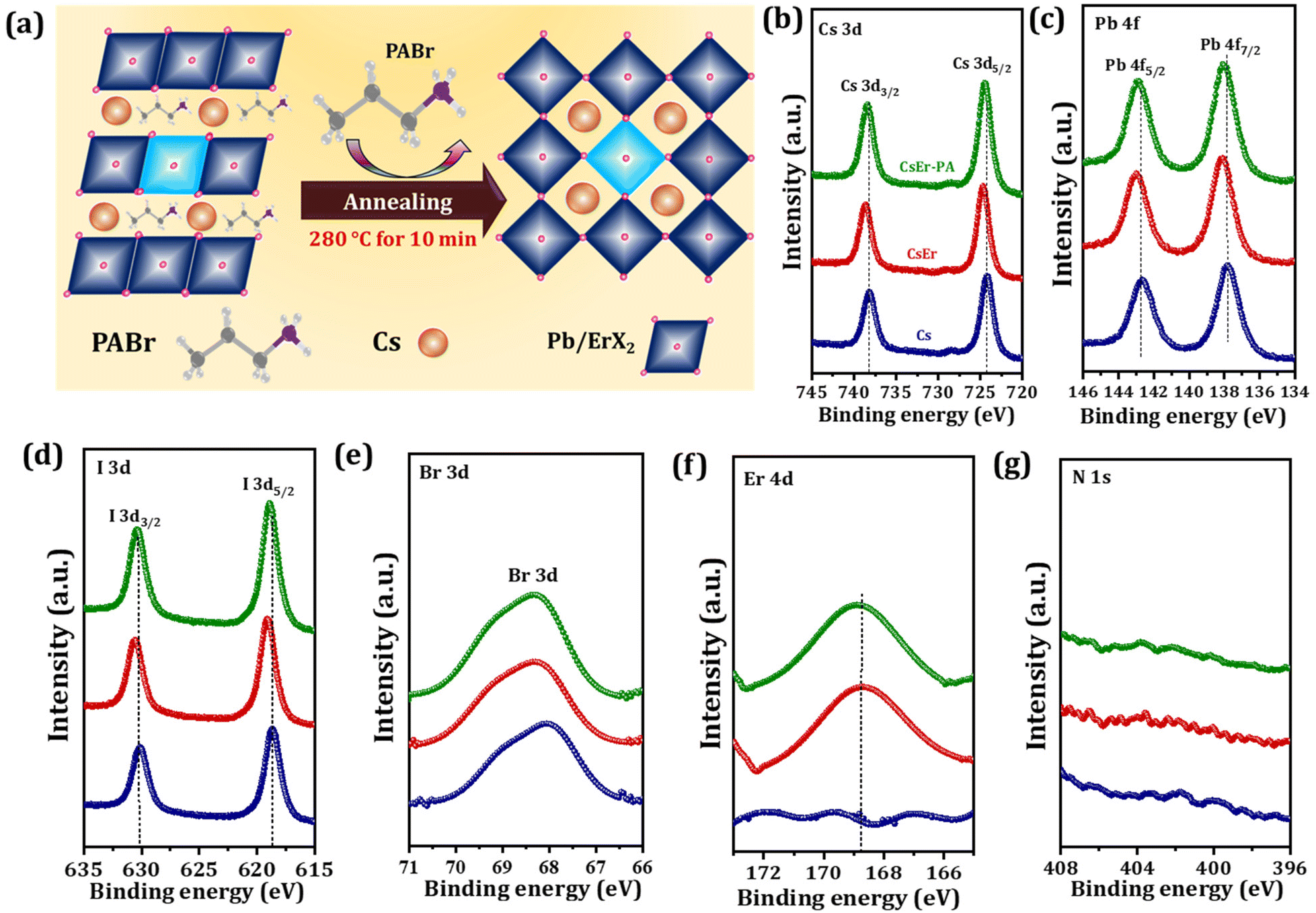 | ||
| Fig. 2 Growth mechanism and chemical composition. (a) Possible growth mechanism. (b–g) XPS spectra of the (b) Cs 3d, (c) Pb 4f, (d) I 3d, (e) Br 3d, (f) Er 4d and (g) N 1s core levels of the Cs, CsEr and CsEr-PA perovskite thin films. | ||
To evaluate the crystal structure phase, optical properties, charge carrier lifetime, and electronic structure, we recorded X-ray diffraction patterns (XRD), time-resolved photoluminescence (TRPL) spectroscopy, UV-Visible spectra, and photoemission spectroscopy (UPS) measurements on Cs, CsEr and CsEr-PA-based perovskite films. Fig. 3(a) displays the XRD patterns of FTO, Cs, CsEr, and CsEr-PA-based perovskite thin films. All corresponding perovskite films exhibited the orthorhombic γ-phase perovskite, which is consistent with our previous reports.17,40,52 Remarkably, the intensity of all peaks of the CsPbI2Br perovskite increased after 3% Er3+ doping and the addition of the PABr additive. In addition, the main peaks of the CsEr and CsEr-PA perovskite films negligibly shifted to a higher angle. Here, due to the close radius of the Er3+ ion (89 pm), it is easy to replace the Pb2+ site (119 pm).27 Fig. S7† shows the magnified peaks of the Cs, CsEr, and CsEr-PA perovskite thin films between 2θ = 12–18° diffraction angle. The highly intense peak shows a highly crystallized CsEr-PA-based perovskite film. Table S2† shows the detailed different structural parameters calculated from the XRD of the corresponding perovskite films. Further, the photoluminescence (PL) (Fig. 3(b)) and TRPL spectroscopy (Fig. 3(c)) of the Cs, CsEr, and CsEr-PA perovskite films were recorded to study the effect of the Er3+ doping and PABr additive on the charge recombination performance. The CsEr-PA film exhibited a higher intensity than the Cs and CsEr perovskite films, proving the effective passivation and decreasing the trap density of the CsEr precursor solution by the addition of the PABr additive. Additionally, the TRPL decay measurements were carried out to check the charge dynamics of the perovskite film after Er3+ doping and PABr additive, as shown in Fig. 3(c). The TRPL decay data were fitted with the tri-exponential decay function from eqn (S1)†54 and detailed parameters are mentioned in Table S3.† The average lifetime of the Cs, CsEr, and CsEr-PA perovskite films was calculated from eqn (S2).† The highest lifetime of τavg = 30 ns was observed for the CsEr-PA-based perovskite film than Cs (τavg = 4.19 ns) and CsEr (τavg = 11 ns) perovskite films. This extended lifetime is achieved due to reduced charge recombination. The band gap values were calculated from the UV-Visible absorption spectra. Fig. 3(d) shows the slight blue shift in the absorption edge for CsEr and CsEr-PA films, resulting in a broadening of the band gap from 1.90 to 1.91 eV (Fig. S8†). Further, we checked the electronic structures in the Cs, CsEr, and CsEr-PA-based films by UPS measurements, as shown in Fig. 3(e). The work function (WF) and valence band maximum (VBM) were calculated by the binding energy cutoff (Ecutoff) and onset (Eonset) (Fig. S9†) and Table S4.† The WF values are 4.19 eV and 4.15 eV and 4.11 eV for the Cs, CsEr, and CsEr-PA perovskite films, respectively. After the Er3+ doping and the addition of the PABr additive in CsPbI2Br, the VBM and conduction band minimum (CBM) places did not change significantly, whereas the WF shifted towards CBM. These outcomes specify the existence of additional negative charge carriers after Er3+ doping and the addition of the PABr additive. Moreover, Er3+ doping and the addition of the PABr additive enlarged the energy level of the CBM (Fig. 3(f)). Notably, the interface charge accumulation loss may be reduced due to Er3+ doping and PABr additive in the CsPbI2Br perovskite and this will benefit enhancing the device performance of IPVSCs.17
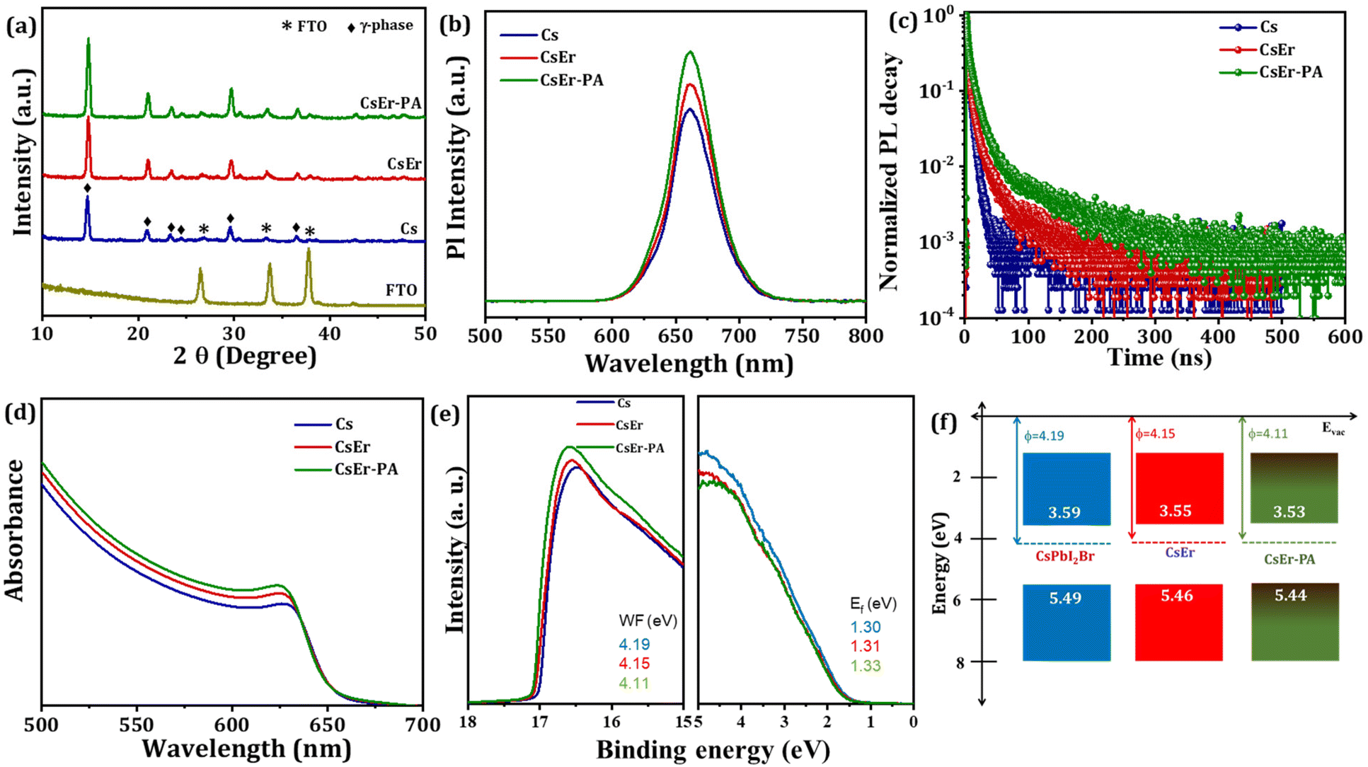 | ||
| Fig. 3 (a) XRD patterns, (b) photoluminescence, (c) time resolved photoluminescence, (d) UV-Vis spectra, (e) UPS analysis (f) energy-level diagram from UV–Vis and UPS measurements of the Cs, CsEr and CsEr-PA perovskite thin films. | ||
To evaluate the photovoltaic performance of different amounts of Er3+ doping and various quantities of PABr additives in the CsPbI2Br perovskite, we fabricated IPVSC devices and recorded their current–voltage (J–V) curves. Fig. S10† shows the J–V curve of the different amounts of PABr (1–3 mg ml−1) additive-added CsPbI2Br (Cs-1 mg ml−1 PABr, Cs-2 mg ml−1 PABr and Cs-3 mg ml−1 PABr) perovskites-based IPVSC and corresponding photovoltaic parameters mentioned in Table S5.† The CsPbI2Br-based perovskite device showed a PCE of 13.20% with an FF of 74.18%, a JSC of 14.45 mAcm−2, and a VOC of 1.235 V. Once we added PABr in the CsPbI2Br perovskite, an increase in photovoltaic performance was observed for 2 mg ml−1 PABr (PCE of 14.72% with a FF of 74.42%, a JSC of 15.69 mAcm−2 and a VOC of 1.261 V). Fig. S11† shows J–V curves of different amounts of Er3+ doping in the CsPbI2Br (CsPb0.99Er0.01I2BrCl0.03, CsPb0.98Er0.02I2BrCl0.06, CsPb0.97Er0.03I2BrCl0.09, and CsPb0.96Er0.04I2BrCl0.12)-based perovskite devices. The related parameters are summarized in Table S6.† When we varied different amounts of Er3+ (x = 0 to 4%) doping in the CsPb1−nErnI2BrXn (X = Cl; 0 ≤ n < 1) perovskite, the highest PCE of 15.73% with FF of 76.79%, JSC of 16.01 mAcm−2 and VOC of 1.280 V were achieved for the CsEr (CsPb0.97Er0.03I2BrCl0.09)-based perovskite device. Furthermore, we varied various concentrations of PABr additives in the optimized CsEr (CsPb0.97Er0.03I2BrCl0.09)-based perovskite. Fig. S12† shows the J–V curves of the CsEr-1 mg ml−1 PABr, CsEr-2 mg ml−1 PABr, CsEr-3 mg ml−1 PABr and CsEr-4 mg ml−1 PABr perovskites-based IPVSC devices and related photovoltaic parameters mentioned in Table S7.† The CsEr-2 mg ml−1 PABr-based device showed a higher PCE than other devices. Fig. 4(a) shows the J–V measurements of the Cs, CsEr, and CsEr-PA-based perovskite devices. Particularly, the CsEr-PA-based device showed a considerable increment in a VOC of 1.304 V, a JSC of 16.16 mAcm−2, a FF of 79.44%, and a PCE of 16.74%, Table 1. This increment is ascribed to the reduced trap density, charge recombination, series resistance, and high-quality thin film by the addition of the PABr additive in the CsEr-based perovskite. Fig. 4(b) shows the external quantum efficiency (EQE) spectra of the Cs, CsEr, and CsEr-PA-based perovskite devices. The EQE values reached were 83%, 88%, and 90% for the Cs, CsEr, and CsEr-PA-based perovskite devices and the corresponding integrated JSC values were 14.23 mAcm−2, 15.38 mA cm−2, and 15.83 mA cm−2, respectively. The resultant integrated JSC values are in good agreement with the JSC extracted from J–V curves. Fig. 4(c) displays the J–V analysis of the champion CsEr-PA-based perovskite device scanned under reverse and forward scans. The corresponding device showed 16.74% PCE for reverse scans and 15.91% PCE for the forward scan, indicating negligible hysteresis. In addition, we investigated the interfacial charge transport performance of the corresponding perovskite devices via the electrochemical impedance spectroscopy (EIS) study. The Nyquist plots of the Cs, CsEr, and CsEr-PA-based perovskite devices and the equivalent circuit model are shown in Fig. 4(d). The EIS-fitted parameters are mentioned in Table S8.† It was found that the CsEr-PA-based perovskite device exhibited a high Rrec of 7857 Ω than the Cs (Rrec = 5337 Ω) and CsEr (Rrec = 6544 Ω)-based perovskite devices, which indicated that the charge recombination was remarkably suppressed in the CsEr-PA-based perovskite device.19
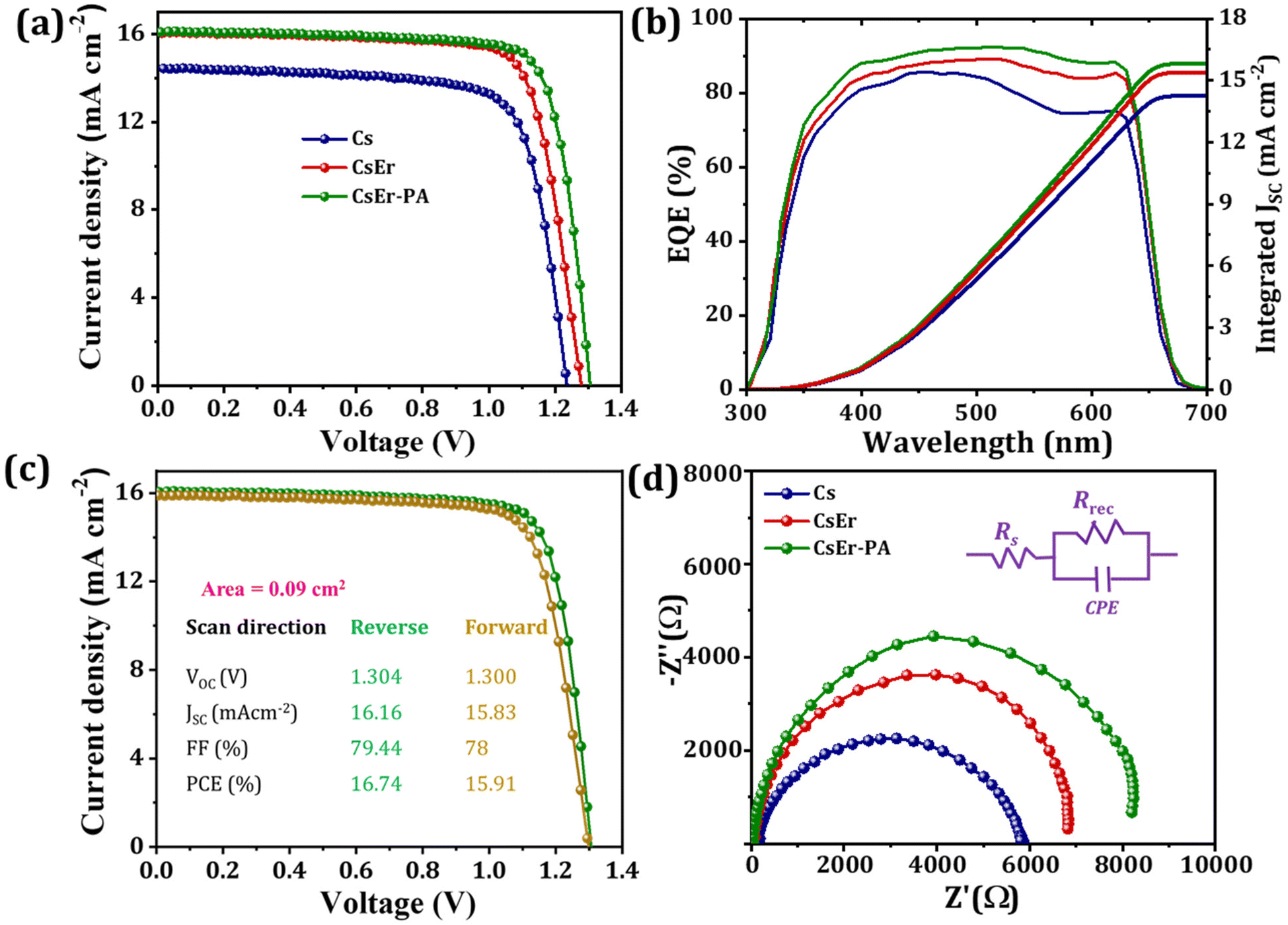 | ||
| Fig. 4 (a) J–V measurements, (b) external quantum efficiency (EQE) of Cs, CsEr and CsEr-PA-based perovskite devices, (c) hysteresis of the champion CsEr-PA-based device, (d) EIS analysis of the Cs, CsEr, CsEr-PA-based perovskite devices. | ||
| Perovskites | V OC (V) | J SC (mA cm−2) | FF (%) | PCE (%) |
|---|---|---|---|---|
| Cs | 1.235 | 14.45 | 74.18 | 13.20 |
| CsEr | 1.280 | 16.01 | 76.79 | 15.73 |
| CsEr-PA | 1.304 | 16.16 | 79.44 | 16.74 |
To study the internal relation between the charge transport and PCE of the device, the charge carrier dynamics of the perovskite devices were measured. Fig. 5(a) shows the ideality factor (η) yielded by the slope of the fitted data, which was calculated using eqn (S3) and (S4).†55,56 Our reference Cs-based device showed η of 1.98 kT q−1 that further decreased to 1.78 kT q−1 and 1.52 kT q−1 for CsEr and CsEr-PA-based devices, respectively, demonstrating the reduction of the charge recombination. Furthermore, to confirm the trap states of the electron-only devices with FTO/mp-TiO2/perovskite/PCBM/Au device configuration, the J–V analysis was carried out under dark conditions, Fig. 5(b). The trap density (Nt) can be calculated according to eqn (S5)†via the trap-filled limit voltage (VTFL).57,58 The trap densities of the Cs, CsEr, and CsEr-PA-based perovskite device are 2.920 × 1016 cm−3, 1.779 × 1016 cm−3 and 1.248 × 1016 cm−3, respectively. This indicates proof of the decreased trap density after the PABr additive, which benefits to reduce the charge recombination and, therefore, results in higher photovoltaic performance observed for the CsEr-PA-based device. The steady-state current density of the CsEr-PA-based IPVSC was measured at a biasing voltage of 1.02 V. Fig. 5(c) exhibited a constant current of 15.72 mAcm−2 with stabilized PCE of 16.03% at over 600 s. Furthermore, the reproducibility of the Cs, CsEr and CsEr-PA-based 15 independent devices was recorded, as shown in Fig. 5(d). Table S9† displays the resultant photovoltaic parameters of the IPVSC devices. We found that the CsEr-PA-based devices exhibited more than 16% average PCE, which was much higher than other Cs and CsEr-based perovskite devices. In addition, the long-term thermal stability of all the Cs, CsEr, and CsEr-PA-based perovskite devices was checked under ambient conditions at ∼25% RH. Fig. 5 shows the thermal long-term stability behavior of the Cs, CsEr, and CsEr-PA-based devices, which were monitored at 65 °C with RH ∼30% without any encapsulation. The CsEr-PA-based perovskite device revealed more stability and retained 90% of its initial PCE of over 400 h. Besides, the CsEr-based devices exhibited lower thermal stability than the champion device. In addition, the thermal stability of the Cs-based devices was lower and the devices started to degrade within 150 h. From the thermal long-term stability investigation, we can confirm that the Er3+-doped and PABr additive-assisted CsPbI2Br perovskite (CsEr-PA)-based device exhibited quite higher long-term stability compared to Cs and CsEr-based perovskite devices. These results were achieved due to the synergistic effect of the optimum amount of Er3+ doping (3% Er3+) and the PABr (2 mg ml−1) additive along with the hot air deposition method. This work delivered a good opportunity to increase the further photovoltaic performance of IPVSC devices.
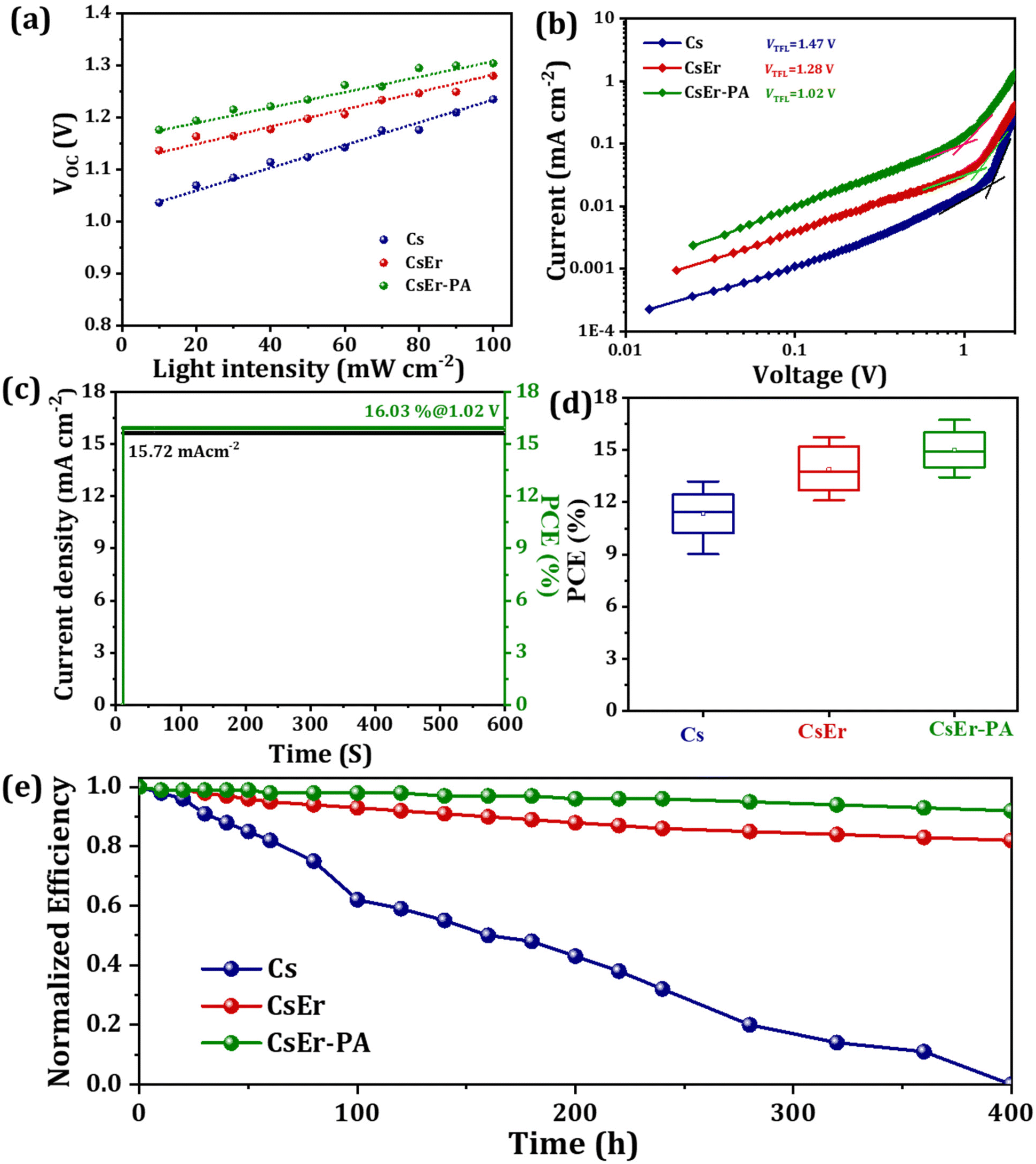 | ||
| Fig. 5 (a) VOC as a function of light intensity, (b) dark current–voltage curves of electron-only devices, (c) steady-state output at the maximum power point tracking (MPPT) of the CsEr-PA-based on the IPVSC, (d) reproducibility of the Cs, CsEr and CsEr-PA-based IPVSC devices and (e) thermal long term stability of Cs, CsEr and CsEr-PA-based IPVSCs without any encapsulation under a ∼25% relative humidity (RH). | ||
3. Conclusions
In conclusion, we developed an effective approach to achieving a high PCE and stable device performance through Er3+ doping and PABr additive in CsPb1−nErnI2BrXn (X = Cl; 0 ≤ n < 1)-based perovskite films. These facile approaches resulted in the CsEr-PA film exhibiting a dense and uniform morphology with a grain size of 1.6 μm. Our champion device containing 3% of Er3+ and 4 mg ml−1 PABr (CsEr-PA) exhibited the highest 16.74%PCE. These optimistic results were achieved due to the reduced trap density, high charge carrier lifetime, and reduced recombination rate. However, Cs (13.20%) and CsEr (15.73%)-based devices showed lower PCE than the champion device. Moreover, the CsEr-PA-based IPVSC device retained 90% of its initial PCE at 400 h for long-term stability.4. Experimental details
Fluorine-doped tin oxide (FTO) substrates were ultrasonically cleaned following the sequence of detergent, distilled water, and ethanol for 15 min for each step and treated with UV plasma for 10 min. The compact-TiO2 (c-TiO2), mesoporous TiO2 (mp-TiO2), TiCl4 treatment, and the CsPbI2Br perovskite precursor solution (1.2 M of CsI, 0.6 M of PbI2 and 0.6 M of PbBr2 in 1 ml of dimethyl sulfoxide (DMSO)) were prepared following a similar process that we reported earlier.12,16,20,42 Furthermore, the stock solution of erbium(III) chloride (ErCl3) was prepared in mixed solvents of DMSO and dimethyl formamide (DMF) (1:2). The CsPb1−nErnI2BrXn (X = Cl; 0 ≤ n < 1) films were synthesized via the addition of the various amounts of the ErCl3 from 0 to 4% into the CsPbI2Br perovskite precursor solution. The prepared films were named as CsPbI2Br, CsPb0.99Er0.01I2BrCl0.03, CsPb0.98Er0.02I2BrCl0.06, CsPb0.97Er0.03I2BrCl0.09, and CsPb0.96Er0.04I2BrCl0.12. In order to balance the perovskite composition, we added exactly an identical amount of CsBr (1.2 M in formamide) to the precursor solution. Further, we added propylammonium bromide (PABr) additive with different amounts from 1 to 4 mg ml−1 in the optimized CsPb1−nErnI2BrXn (X = Br or Cl; 0 ≤ n < 1) perovskite precursor solution. Later, this perovskite solution was spun first at 1000 rpm for 10 s and then at 3000 rpm for 30 s. The hot air was blown over the spinning substrate for 10 s after spinning at 3000 rpm. All Cs (CsPbI2Br), CsEr (CsPb0.97Er0.03I2BrCl0.09), and CsEr-PA (CsPb0.97Er0.03I2BrCl0.09 − 2 mg ml−1 PABr)-based films were annealed at 280 °C for 10 min. To prepare a hole-transporting layer (HTL) (P3HT solution) and a gold (Au) by thermal evaporation to complete the IPVSC, we followed our previous reports.12,16,20
Conflicts of interest
The authors declare no competing financial interests.Acknowledgements
This work was supported by Priority Research Centre Program through the National Research Foundation of Korea (NRF) funded by the Ministry of Education, Science, and Technology (NRF-2018R1A6A1A03024334) and (2020R1A2C2004880).References
- M. H. Kumar, S. Dharani, W. L. Leong, P. P. Boix, R. R. Prabhakar, T. Baikie, C. Shi, H. Ding, R. Ramesh, M. Asta, M. Gratzel, S. G. Mhaisalkar and N. Mathews, Lead-free halide perovskite solar cells with high photocurrents realized through vacancy modulation, Adv. Mater., 2014, 26, 7122 CrossRef CAS PubMed.
- Y. Wang, M. I. Dar, L. K. Ono, T. Zhang, M. Kan, Y. Li, L. Zhang, X. Wang, Y. Yang, X. Gao, Y. Qi, M. Gratzel and Y. Zhao, Thermodynamically stabilized β-CsPbI3-based perovskite solar cells with efficiencies >18, Science, 2019, 365, 591–595 CrossRef CAS PubMed.
- J. Duan, Y. Zhao, X. Yang, Y. Wang, B. He and Q. Tang, Lanthanide ions doped CsPbBr3 halides for HTM-free 10.14%-efficiency inorganic perovskite solar cell with an ultrahigh open-circuit voltage of 1.594 V, Adv. Energy Mater., 2018, 8, 1802346 CrossRef.
- J. Zhang, G. Hodes, Z. Jin and S. Liu, All-inorganic CsPbX3 perovskite solar cells: progress and prospects, Angew. Chem., Int. Ed., 2018, 58, 15618 Search PubMed.
- X. Gong, L. Guan, H. Pan, Q. Sun, X. Zhao, H. Li, H. Pan, Y. Shen, Y. Shao, L. Sun, Z. Cui, L. Ding and M. Wang, Highly efficient perovskite solar cells via nickel passivation, Adv. Funct. Mater., 2018, 28, 1804286 CrossRef.
- L. Zhou, X. Guo, Z. Lin, J. Ma, J. Su, Z. Hu, C. Zhang, S. F. Liu, J. Chang and Y. Hao, Interface engineering of low temperature processed all-inorganic CsPbI2Br perovskite solar cells toward PCE exceeding 14%, Nano Energy, 2019, 60, 590 Search PubMed.
- J. Xue, R. Wang, K. L. Wang, Z. K. Wang, I. Yavuz, Y. Wang, Y. Yang, X. Gao, T. Huang, S. Nuryyeva, J. W. Lee, Y. Duan, L. S. Liao, R. Kaner and Y. Yang, Crystalline liquid-like behavior: surface-induced secondary grain growth of photovoltaic perovskite thin film, J. Am. Chem. Soc., 2019, 141, 13948–13953 CrossRef CAS PubMed.
- H. Zhao, J. Xu, S. Zhou, Z. Li, B. Zhang, X. Xia, X. Liu, S. Dai and J. Yao, Preparation of tortuous 3D γ-CsPbI3 films at low temperature by CaI2 as dopant for highly efficient perovskite solar cells, Adv. Funct. Mater., 2018, 29, 1808986 Search PubMed.
- S. M. Yoon, H. Min, J. B. Kim, G. Kim, K. S. Lee and S. I. Seok, Surface engineering of ambient-air-processed cesium lead triiodide layers for efficient solar cells, Joule, 2021, 5, 196 CrossRef.
- Y. Wang, T. Zhang, M. Kan and Y. Zhao, Bifunctional Stabilization of all-inorganic α-CsPbI3 perovskite for 17% efficiency photovoltaics, J. Am. Chem. Soc., 2018, 140, 12345–12348 CrossRef CAS PubMed.
- R. J. Sutton, G. E. Eperon, L. Miranda, E. S. Parrott, B. A. Kamino, J. B. Patel, M. T. Horantner, M. B. Johnston, A. A. Haghighirad, D. T. Moore and H. J. Snaith, Bandgap- tunable cesium lead halide perovskites with high thermal stability for efficient solar cells, Adv. Energy Mater., 2016, 6, 1502458 CrossRef.
- J. V. Patil, S. S. Mali and C. K. Hong, A-Site rubidium cation-incorporated CsPbI2Br all- inorganic perovskite solar cells exceeding 17% efficiency, Sol. RRL, 2020, 2000164 CrossRef CAS.
- Y. Guo, F. Zhao, J. Tao, J. Jiang, J. Zhang, J. Yang, Z. Hu and J. Chu, Efficient and hole- transporting-layer-free CsPbI2Br planar heterojunction perovskite solar cells through rubidium passivation, ChemSusChem, 2019, 12, 983 CrossRef CAS PubMed.
- J. K. Nam, S. U. Chai, W. Cha, Y. J. Choi, W. Kim, M. S. Jung, J. Kwon, D. Kim and J. H. Park, Potassium incorporation for enhanced performance and stability of fully inorganic cesium lead halide perovskite solar cells, Nano Lett., 2017, 17, 2033 CrossRef PubMed.
- A. Kausar, A. Sattar, C. Xu, S. Zhang, Z. Kang and Y. Zhang, Advent of alkali metal doping: a roadmap for the evolution of perovskite solar cells, Chem. Soc. Rev., 2021, 50, 2736 RSC.
- S. S. Mali, J. V. Patil, S. R. Rondiya, N. Y. Dzade, J. A. Steele, M. K. Nazeerudin, P. S. Patil and C. K. Hong, Terbium-doped and dual-passivated γ-CsPb(I1−xBrx)3 inorganic perovskite solar cells with improved air thermal stability and high efficiency, Adv. Mater., 2022, 34, 2203204 CrossRef CAS PubMed.
- S. S. Mali, J. V. Patil, J. A. Steele, S. R. Rondiya, N. Y. Dzade and C. K. Hong, Implementing dopant-free hole-transporting layers and metal-incorporated CsPbI2Br for stable all-inorganic perovskite solar cells, ACS Energy Lett., 2021, 6, 788 Search PubMed.
- J. V. Patil, S. S. Mali and C. K. Hong, Boosting the stability of fully-inorganic perovskite solar cells through samarium doped CsPbI2Br perovskite, ACS Sustainable Chem. Eng., 2020, 8, 16371 Search PubMed.
- J. V. Patil, S. S. Mali and C. K. Hong, Hot-air-assisted fully air-processed barium incorporated CsPbI2Br perovskite thin films for highly efficient and stable all-inorganic perovskite solar cells, Nano Lett., 2019, 19, 6213–6220 CrossRef PubMed.
- J. V. Patil, S. S. Mali and C. K. Hong, Efficient and stable all-inorganic niobium-incorporated CsPbI2Br-based perovskite solar cells, ACS Appl. Mater. Interfaces, 2020, 12, 27183 Search PubMed.
- Z. Zeng, Y. Xu, Z. Zhang, Z. Gao, M. Luo, Z. Yin, C. Zhang, J. Xu, B. Huang, F. Luo, Y. Du and C. Yan, Rare-earth-containing perovskite nanomaterials: design, synthesis, properties and applications, Chem. Soc. Rev., 2020, 49, 1109–1143 RSC.
- J. V. Patil, S. S. Mali and C. K. Hong, Fully-inorganic strontium incorporated CsPbI2Br perovskite solar cells with promoted efficiency and stability, J. Energy Chem., 2021, 62, 458 Search PubMed.
- S. Xiang, W. Li, Y. Wei, J. Liu, H. Liu, L. Zhu, S. Yang and H. Chen, Natrium noping pushes the efficiency of carbon-based CsPbI3 perovskite solar cells to 10.7%, iScience, 2019, 15, 156 CrossRef CAS PubMed.
- G. Pan, X. Bai, D. Yang, X. Chen, P. Jing, S. Qu, L. Zhang, D. Zhou, J. Zhu, W. Xu, B. Dong and H. Song, Doping lanthanide into perovskite nanocrystals: highly improved and expanded optical properties, Nano Lett., 2017, 17, 8005 CrossRef CAS PubMed.
- X. Zhang, X. Ren, B. Liu, R. Munir, X. Zhu, D. Yang, J. Li, Y. Liu, D.-M. Smilgies, R. Li, Z. Yang, T. Niu, X. Wang, A. Amassian, K. Zhao and S. Liu, Stable high efficiency two-dimensional perovskite solar cells via cesium doping, Energy Environ. Sci., 2017, 10, 2095 RSC.
- Z. Zeng, B. Huang, X. Wang, L. Lu, Q. Lu, M. Sun, T. Wu, T. Ma, J. Xu, Y. Xu, S. Wang, Y. Du and C. H. Yan, Multimodal luminescent Yb3+/Er3+/Bi3+-doped perovskite single crystals for X-ray detection and anti-counterfeiting, Adv. Mater., 2020, 32, 2004506 CrossRef CAS PubMed.
- J. Duan, Y. Zhao, X. Yang, Y. Wang, B. He and Q. Tang, Lanthanide ions doped CsPbBr3 halides for HTM-Free 10.14%-efficiency inorganic perovskite solar cell with an ultrahigh open-circuit voltage of 1.594 V, Adv. Energy Mater., 2018, 8, 1802346 CrossRef.
- T. Cai, J. Wang, W. Li, K. Hills-Kimball, H. Yang, Y. Nagaoka, Y. Yuan, R. Zia and O. Chen, Mn2+/Yb3+ Codoped CsPbCl3 perovskite nanocrystals with triple-wavelength emission for luminescent solar concentrators, Adv. Sci., 2020, 7, 2001317 CrossRef CAS PubMed.
- R. Sun, D. Zhou and H. Song, Rare earth doping in perovskite luminescent nanocrystals and photoelectric devices, Nano Sel., 2022, 3, 531–554 CrossRef CAS.
- W. Zhao, Z. Yao, F. Yu, D. Yang, S. Liu, X. Chen, J. Xu, Y. Xu, F. Luo and Y. Du, Rare earth double perovskites: a fertile soil in the field of perovskite oxides, Inorg. Chem. Front., 2019, 6, 2226–2238 RSC.
- M. Que, W. Que, X. Yin, P. Chen, Y. Yang, J. Hu, B. Yub and Y. Du, Enhanced conversion efficiency in perovskite solar cells by effectively utilizing near infrared light, Nanoscale, 2016, 8, 14432–14437 RSC.
- J. Shi, F. Li, J. Yuan, X. Ling, S. Zhou, Y. Qian and W. Ma, Efficient and stable CsPbI3 perovskite quantum dots enabled by in situ ytterbium doping for photovoltaic applications, J. Mater. Chem. A, 2019, 7, 20936 RSC.
- Z. Song, W. Xu, Y. Wu, S. Liu, W. Bi, X. Chen and H. Song, Incorporating of lanthanides ions into perovskite film for efficient and stable perovskite solar cells, Small, 2020, 16, 2001770 CrossRef CAS PubMed.
- S. Rong, Y. Xiao, J. Jiang, Q. Zeng and Y. Li, Strongly enhanced photoluminescence and photoconductivity in erbium-doped MAPbBr3 single crystals, J. Phys. Chem. C, 2020, 124, 8992 CrossRef CAS.
- A. Polman, Erbium implanted thin film photonic materials, J. Appl. Phys., 1997, 82, 1–39 CrossRef CAS.
- Z. Zeng, Y. Xu, Z. Zhang, Z. Gao, M. Luo, Z. Yin, C. Zhang, J. Xu, B. Huang, F. Luo, Y. Du and C. Yan, Rare-earth-containing perovskite nanomaterials :design, synthesis, properties and applications, Chem. Soc. Rev., 2020, 49, 1109–1143 RSC.
- X. Chen, J. Xu, Y. Xu, F. Luo and Y. Du, Rare earth double perovskites: a fertile soil in the field of perovskite oxides, Inorg. Chem. Front., 2019, 6, 2226–2238 RSC.
- Y. Cheng and K. Sun, Color modification of ZnGa2O4:Yb33+, Er3+,Tm3+ upconversion phosphors with the doping of Sn4+ and Ge4+ ions, Appl. Opt., 2020, 59, 7313–7320 CrossRef CAS PubMed.
- L. Liu, S. Wang, B. Zhao, P. Pei, Y. Fan, X. Li and F. Zhang, Er3+ Sensitized 1530 nm to 1180 nm second near-infrared window upconversion nanocrystals for in vivo biosensing, Angew. Chem., Int. Ed., 2018, 57, 7518–7522 CrossRef CAS PubMed.
- J. V. Patil, S. S. Mali and C. K. Hong, Grain size enlargement and controlled crystal growth by formamidinium chloride added γ-CsPbI2Br-based stable inorganic perovskite solar cells, Mater. Today Chem., 2022, 26, 101118 CrossRef CAS.
- J. Ma, M. Qin, Y. Li, T. Zhang, J. Xu, G. Fang and X. Lu, Guanidinium doping enabled low-temperature fabrication of high-efficiency all-inorganic CsPbI2Br perovskite solar cells, J. Mater. Chem. A, 2019, 7, 27647 Search PubMed.
- J. V. Patil, S. S. Mali and C. K. Hong, Reducing defects of all-inorganic γ-CsPbI2Br thin films by ethylammonium bromide additives for efficient perovskite solar cells, ACS Appl. Mater. Interfaces, 2022, 14, 25583 Search PubMed.
- Y. Lin, Y. Bai, Y. Fang, Z. Chen, S. Yang, X. Zheng, S. Tang, Y. Liu, J. Zhao and J. Huang, Enhanced thermal stability in perovskite solar cells by assembling 2D/3D stacking Structures, J. Phys. Chem. Lett., 2018, 9, 658 Search PubMed.
- K. Wang, J. Zhou, X. Li, N. Ahmad, H. Xia, G. Wu, X. Zhang, B. Wang, D. Zhang, Y. Zou, H. Zhou and Y. Zhang, A surface modifier enhances the performance of the all- inorganic CsPbI2Br perovskite solar cells with efficiencies approaching 15%, Phys. Chem. Chem. Phys., 2020, 22, 17856 Search PubMed.
- S. Fu, X. Li, L. Wan, W. Zhang, W. Song and J. Fang, Effective surface treatment for high- performance inverted CsPbI2Br perovskite solar cells with efficiency of 15.92%, Nano-Micro Lett., 2020, 12, 170 CrossRef CAS PubMed.
- K. S. Kim, I. S. Jin, S. H. Park, S. J. Lim and J. W. Jung, Methylammonium iodide- Mediated controlled crystal growth of CsPbI2Br films for efficient and stable all- inorganic perovskite solar cells, ACS Appl. Mater. Interfaces, 2020, 12, 36236 Search PubMed.
- J. V. Patil, S. S. Mali and C. K. Hong, A thioacetamide additive-based hybrid (MA0.5FA0.5)PbI3 perovskite solar cells crossing 21% efficiency with excellent long term stability, Mater. Today Chem., 2020, 25, 100950 CrossRef.
- X. Hou, Y. Hu, H. Liu, A. Mei, X. Li, M. Duan, G. Zhang, Y. Rong and H. Han, Effect of guanidinium on mesoscopic perovskite solar cells, J. Mater. Chem. A, 2017, 5, 78 Search PubMed.
- K. L. Wang, R. Wang, Z. K. Wang, M. Li, Y. Zhang, H. Ma, L. S. Liao and Y. Yang, Tailored phase transformation of CsPbI2Br films by copper(II) bromide for high- performance all-inorganic perovskite solar cells, Nano Lett., 2019, 19, 5184 Search PubMed.
- Y. Han, H. Zhao, C. Duan, S. Yang, Z. Yang, Z. Liu and S. (Frank) Liu, Controlled n- doping in air-stable CsPbI2Br perovskite solar cells with a record efficiency of 16.79%, Adv. Funct. Mater., 2020, 30, 1909972 CrossRef CAS.
- T. Li, Y. Pan, Z. Wang, Y. Xia, Y. Chen and W. Huang, Additive engineering for highly efficient organic–inorganic halide perovskite solar cells: recent advances and perspectives, J. Mater. Chem. A, 2017, 5, 12652 Search PubMed.
- J. V. Patil, S. S. Mali, D. W. Park and C. K. Hong, Novel ytterbium-doped CsPbI2Br thin- films–based inorganic perovskite solar cells toward improved phase stability, Mater. Today Chem., 2021, 22, 100557 CrossRef CAS.
- C. Yi, J. Luo, S. Meloni, A. Boziki, N. Ashari-Astani, C. Gratzel, S. M. Zakeeruddin, U. Rothlisberger and M. Gratzel, Entropic stabilization of mixed A-cation ABX3 metal halide perovskites for high performance perovskite solar cells, Energy Environ. Sci., 2016, 9, 656 RSC.
- S. S. Mali, J. V. Patil, H. J. Kim and C. K. Hong, Gallium cationic incorporated compact TiO2 as an efficient electron-transporting layer for stable perovskite solar cells, Matter, 2019, 1, 464 CrossRef.
- C. G. Shuttle, B. O. Regan, A. M. Ballantyne, J. Nelson, D. D. Bradley and J. R. Durrant, Bimolecular recombination losses in polythiophene: fullerene solar cells, Phys. Rev. B: Condens. Matter Mater. Phys., 2008, 78, 113201 CrossRef.
- H. Wang, J. H. Hsu, G. Yang and C. Yu, Novel organic schottky barrier diode created in a single planar polymer film, Adv. Mater., 2016, 28, 9549 Search PubMed.
- H. Y. Park, D. C. Lim, K. D. Kim and S. Y. Jang, Performance optimization of low-temperature- annealed solution-processable ZnO buffer layers for inverted polymer solar cells, J. Mater. Chem. A, 2013, 1, 6334 Search PubMed.
- J. Zhu, B. He, Z. Gong, Y. Ding, W. Zhang, X. Li, Z. Zong, H. Chen and Q. Tang, Grain enlargement and defect passivation with melamine additives for high efficiency and stable CsPbBr3 perovskite solar cells, ChemSusChem, 2020, 13, 1843 Search PubMed.
Footnote |
| † Electronic supplementary information (ESI) available: The detailed procedures for all characterization techniques are given in the supporting information. See DOI: https://doi.org/10.1039/d2qi02448a |
| This journal is © the Partner Organisations 2023 |