
 Open Access Article
 This Open Access Article is licensed under a Creative Commons Attribution-Non Commercial 3.0 Unported Licence
Potential of AlP and GaN as barriers in magnetic tunnel junctions
Gokaran
Shukla
*,
Hasan M.
Abdullah
and
Udo
Schwingenschlögl
 *
*
King Abdullah University of Science and Technology (KAUST), Physical Science and Engineering Division (PSE), Thuwal 23955-6900, Saudi Arabia. E-mail: gokaran.shukla@kaust.edu.sa; udo.schwingenschlogl@kaust.edu.sa
First published on 13th September 2023
Abstract
AlP and GaN are wide band gap semiconductors used industrially in light emitting diodes. We investigate their potential as tunnel barriers in magnetic tunnel junctions, employing density functional theory and the non-equilibrium Green's function method for ground state and quantum transport calculations, respectively. We show that the valence band edges are dominated by pz orbitals and the conduction band edges are dominated by s orbitals. Both materials filter Bloch states of Δ1 symmetry at the Γ-point of the Brillouin zone. In the zero bias limit, we find for the Co/AlP/Co junction a high tunnel magnetoresistance of ∼200% at the Fermi energy and for the Co/GaN/Co junction a tunnel magnetoresistance of even ∼300% about 1.4 eV below the Fermi energy.
I. Introduction
While the first evidence of anisotropic magnetoresistance was established by Lord Kelvin in Fe,1 in the early seventies of the last century tunneling magnetoresistance (TMR) was reported for the Fe/Ge/Co junction at 4 K.2 However, mainly the discovery of giant magnetoresistance3,4 expedited the field of spintronics and now is one of its backbones. In giant magnetoresistance devices a non-magnetic metal, such as Cu or Pt, is sandwiched between ferromagnetic electrodes, offering two resistance states depending on the spin alignment of the electrodes. In TMR devices the non-magnetic metal is replaced with an insulator.5 An electron tunneling through the barrier encounters different resistance depending on the Bloch state symmetry and spin alignment of the electrodes.In the case of incoherent transport the TMR depends on the spin-polarizations P1/2 = (D↑ − D↓)/(D↑ + D↓) of the electrodes (1) and (2) as
| TMR = 2P1P2/(1 − P1P2), | (1) |
In the case of coherent transport the TMR depends on the tunnel currents IP and IAP under parallel (P) and antiparallel (AP) spin alignments of the electrodes as
| TMR = (IP − IAP)/IAP. | (2) |
After a TMR of ∼230% was found at room temperature,11,12 Fe/MgO/Fe junctions were adopted for applications such as spin-transfer torque devices,13,14 microwave generators,15 non-volatile full adders,16 non-volatile field programming gate arrays,17 non-volatile flip-flops,18–20 static random access memories,21 comparators,22 neuromorphic computers,23–26 magnetic read heads,27 non-uniform clock generators,28 sensors,29,30 analog-to-digital converters,31–33 not-and gates,34 embedded memories,35 radio-frequency spectrum optimizers,36 and oscillators.37
While symmetry filtering is a general concept applicable to a variety of interfaces such as Co2MnSi/MgO,38 SrTiO3/BaTiO3,39 Cu/EuO,40 Co/h-BN,41 Fe/HfO2,42 and Co/SiO2,42 only the FeCoB/MgO interface is currently used in main-stream applications. This is partially due to the possibility of B-assisted epitaxial growth of the Fe/MgO/Fe junction, which enables high transmission of spin-polarized current. The generation and detection of spin-polarized current are principal prerequisites for any spintronics device. While the Fe/MgO/Fe junction plays a central role on this front, it suffers from disadvantages in fabrication, as the four-fold rotationally symmetric MgO must be grown on the six-fold rotationally symmetric face centered cubic [111] plane of the Ir–Mn/Co–Fe/Ru/Fe stack. Both Co and Ni provide the required six-fold rotation symmetry.43 Moreover, the rather large Gilbert damping of the ferromagnets Fe and Co (ref. 44) impedes the magnetic quantum bit flipping by spin transfer torque in magnetoresistive random-access memories and the microwave generation by precession of the magnetic moment, for example.
Semiconductor junctions, on the other hand, offer new functionalities for optoelectronics and magnetic quantum bit devices to be potentially integrated with the current complementary metal–oxide semiconductor technology, bring memory elements close to logic elements, and help to realize spin-based displays.45 In valleytronics the valley dependence of a spin-polarized current, mostly due to the broken inversion symmetry in crystal structures such as wurzite, is exploited.46 It is therefore vital to explore new tunnel barrier materials to achieve junctions that can operate at or above room temperature with high TMR and provide high spin-polarized current. For this reason, we present here a detailed theoretical analysis of junctions based on the wurzite crystal structure using AlP or GaN as tunnel barrier and Co, Ni, or Fe as ferromagnetic electrodes. AlP and GaN are wide band gap semiconductors that are extensively used in the optoelectronics industry in light emitting diodes, whereas Co, Ni, and Fe are strong ferromagnets with high Curie temperatures. Analyzing such junctions has the potential to open new avenues in spintronics.
The paper is organized as follows: we first introduce our methodology and the technical details of our calculations. Then we discuss the real and complex band structures of the tunnel barriers and electrodes. Afterwards, we analyze the TMR and present our conclusions.
II. Computational details
We employ Kohn–Sham density functional theory for performing ground state electronic structure calculations. The exchange–correlation potential is treated in the local density approximation as parameterized by Ceperley and Alder.47 The Siesta engine is used with norm-conserving non-relativistic Troullier–Martins pseudopotentials48 and a localized atomic-orbital basis set. The s, p, and d orbitals of Co, Ni, and Fe are expanded in a double-ζ basis set, while the s and p orbitals of Al, P, Ga, and N are expanded in a double-ζ plus polarization basis set. The band gaps of AlP and GaN are improved by the atomic self-interaction correction.49,50 We use a grid spacing equivalent to a plane wave cutoff of 400 Ryd and a Monkhorst–Pack 8 × 8 × 8 k-mesh. The complex band structure along the z-direction is derived from the secular equation with k‖ = 0, i.e., sampling is not required along this direction.We study the
• Co[0001]/AlP[0001]/Co[0001],
• Ni[0001]/AlP[0001]/Ni[0001],
• Co[111]/GaN[0001]/Co[111], and
• Fe[001]/GaN[001]/Fe[001]
junctions seen in Fig. 1. The Co/AlP/Co and Ni/AlP/Ni junctions are constructed from hexagonal close packed (hcp) AlP with the in-plane lattice constant compressed by 2.8% from 3.86 Å (optimized value in the local density approximation) to 3.75 Å to achieve epitaxy between 2 × 2 AlP[0001] and 3 × 3 hcp-Co[0001] (lattice constant 2.50 Å (ref. 51)) or hcp-Ni[0001] (lattice constant 2.50 Å in the local density approximation). The Co/GaN/Co junction is constructed from wurzite GaN with the in-plane lattice constant stretched by 4.9% from 3.19 Å (ref. 52) to 3.34 Å to achieve epitaxy between 2 × 2 GaN[0001] and 3 × 3 body centered cubic (bcc) Co[111] with the in-plane lattice constant compressed by 4.5% from 2.86 Å (ref. 53) to 2.73 Å. The Fe/GaN/Fe junction is constructed from zinc blende GaN (lattice constant 4.50 Å (ref. 54)) by achieving epitaxy between 2 × 2 GaN[001] and 3 × 3 bcc-Fe[001] with the in-plane lattice constant stretched by 4.8% from 2.86 Å (ref. 53) to 3.00 Å. The thicknesses of the AlP[0001], GaN[0001], and GaN[001] tunnel barriers are chosen as 22.5, 16.1, and 24.8 Å, respectively (four unit cells). By structural relaxation using the conjugate gradient method, we reduce the forces acting on the atoms in the junctions to less than 0.01 eV Å−1. The junctions are asymmetric with broken inversion symmetry, which lifts the spin transmission degeneracy for AP spin alignment of the electrodes.
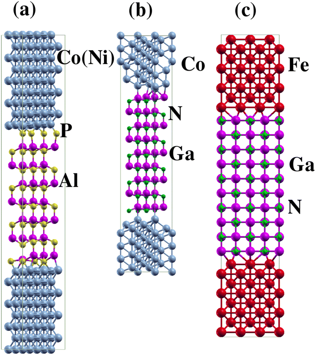 | ||
| Fig. 1 Structures of the (a) Co/AlP/Co and Ni/AlP/Ni, (b) Co/GaN/Co, and (c) Fe/GaN/Fe junctions. The junctions are asymmetric with broken inversion symmetry, resulting in different chemical environments at the two ends of the tunnel barrier. | ||
For performing transport calculations, we employ the Smeagol engine,55–57 which is interfaced with the Siesta engine and adopts the non-equilibrium Green's function method. In this formalism the left/right (L/R) electrode is described by a complex self-energy  , where σ = ↑ or ↓ is the spin and E is the energy. The effective Green's function of the central scattering region then is given by
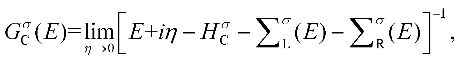 | (3) |
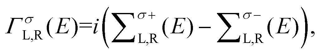 | (4) |
| Tσ(E) = Tr[ΓσL(E)Gσ†C(E)ΓσR(E)GσC(E)]. | (5) |
As the junction is translationally invariant in the transverse plane, we can write:
 | (6) |
 is the k‖-dependent transmission coefficient. From the transmission coefficients TP(E) and TAP(E) under P and AP spin alignments of the electrodes, we obtain
| TMR = (TP(E) − TAP(E))/TAP(E), | (7) |
| TP/AP(E) = T↑P/AP(E) + T↓P/AP(E). | (8) |
The transport calculations are performed with a density matrix converged to a tolerance of 10–4. Tσ(E) is then calculated using a 50 × 50 × 1 k-mesh. We notice no significant change in Tσ(E) or the TMR for a 100 × 100 × 1 k-mesh.
III. Results and discussion
A. AlP and GaN as tunnel barriers
The band gaps of 1.5 eV (indirect) for AlP and 0.8 eV (direct) for GaN obtained in the local density approximation strongly underestimate the experimental values of 2.5 eV (ref. 58) and 3.3 eV,59 respectively, while the atomic self-interaction correction improves them to 2.2 and 2.6 eV. These values are reduced to 1.5 and 2.0 eV, respectively, under the applied strains, while the band dispersions at the valence and conduction band edges remain similar (and are not critical in the tunneling regime) and the symmetries of the Bloch states are preserved. The symmetries of the Bloch states are also preserved for bcc-Fe and bcc-Co under the applied strains. The complex wave vector in the tunnel barrier is given by (kz = iκ):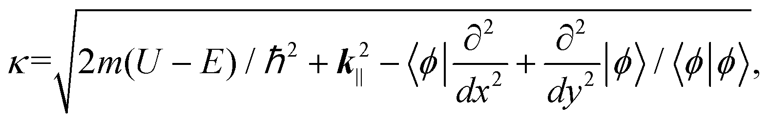 | (9) |
We plot κ(EF, k‖) in Fig. 2 to establish the high transmission regions dominating the tunnel current. Minima at the Γ-point correspond to the situation that the tunneling electrons approach the barrier in normal direction, i.e., the effective barrier thickness is minimal. While Γ-point driven transport is neither a necessary nor a sufficient condition for a high TMR, the typical parabolic energy dispersions around the Γ-point often result in Δ1 symmetry of the Bloch states along the transport direction. Complying with this symmetry condition severely constrains the selection of ferromagnets. The decay of the evanescent states is similar in AlP and GaN due to the similar band gaps and electronic couplings, with the valence band edges dominated by pz orbitals and the conduction band edges dominated by s orbitals. Note that the size of the band gap affects the magnitude of κ(EF, k‖) but not the distribution in the BZ. Therefore, it affects the magnitude of T(E) but not the underlying physics.
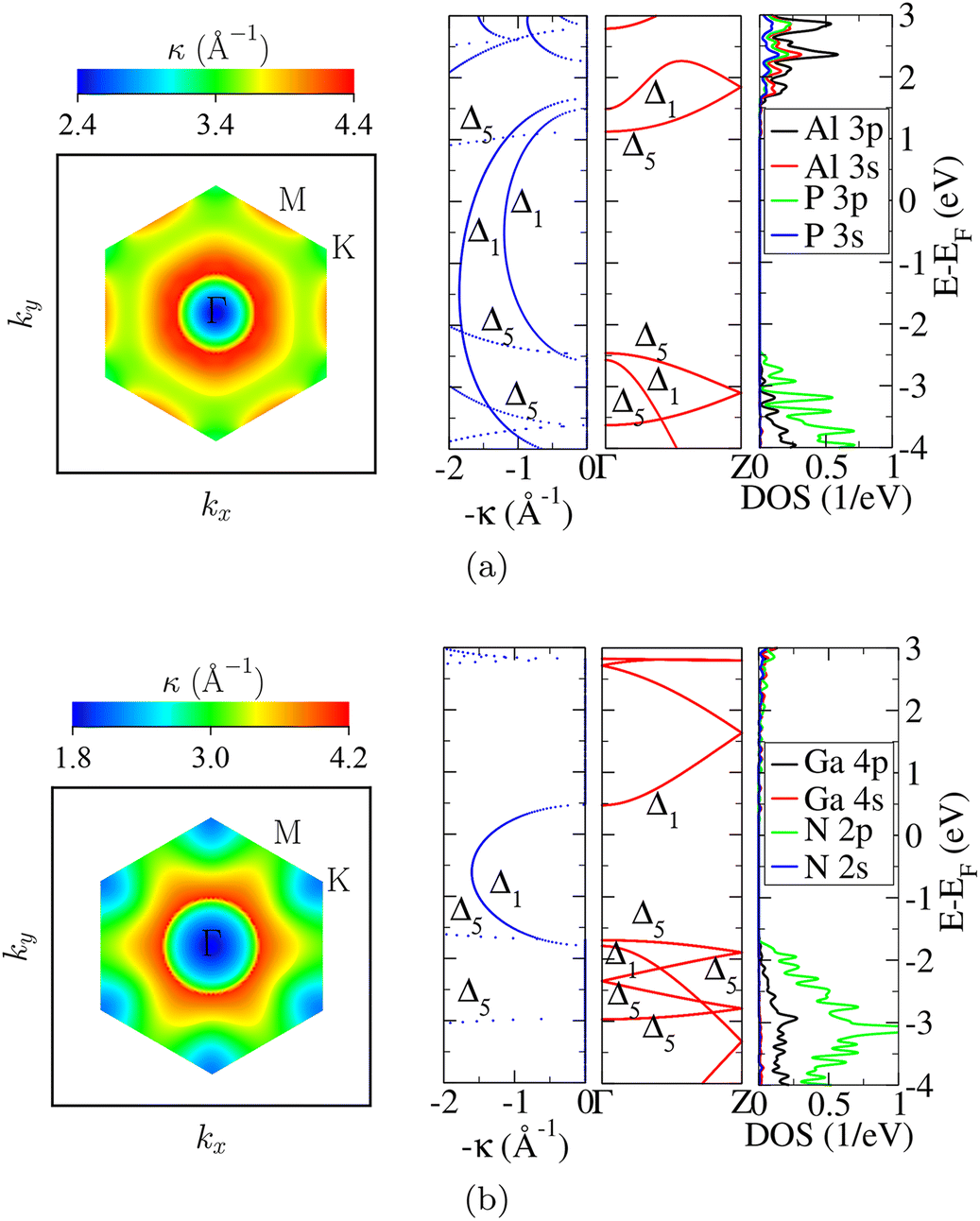 | ||
| Fig. 2 Electronic structure analyses of (a) AlP and (b) GaN. The left panel shows a heat map of κ(EF, k‖) in the BZ, reaching from the minimal to the maximal value. The right panels show the real (red) and complex (blue) band structures along the [0001] direction as well as partial densities of states. | ||
Next we analyze the real and complex band structures along the transport direction to relate them later with those of the electrodes. Generally, in epitaxial junctions the spin–flip and interband scatterings are minimal. As the same symmetry of the Bloch states is required to tunnel through the barrier, a strong coupling of the electrodes with the valence and conduction band edges of the semiconductor results in a high current. If only one spin channel of the ferromagnet is present at EF then a highly spin-polarized current is expected. Note that our analysis of T(E) in terms of the electronic bands and their symmetry at the Γ-point is only qualitative, because the entire BZ contributes to T(E). However, the main contribution is due to the region around the Γ-point, since there κ(EF, k‖) is minimal.
The symmetry of a Bloch state is assigned by analyzing its orbital composition after projecting it into the xy-plane (perpendicular to the transport direction). In particular, Δ1 symmetry corresponds to s, pz, and d3z2−r2 orbitals with zero angular momentum in the transport direction, Δ5 symmetry to px, py, dxz, and dyz orbitals, Δ2 symmetry to dx2−y2 orbitals, and Δ2′ symmetry to dxy orbitals. The symmetries of the different bands at the Γ-point are shown in the real and complex band structures of AlP and GaN in Fig. 2. We find no ghost states in the complex band structures, which can appear for a non-orthogonal basis set.60 Both semiconductors filter Δ1 symmetry at the Γ-point. In the case of AlP, a valence band of Δ1 symmetry with weak decay in the tunnel barrier connects to close to the conduction band edge. A valence band of Δ5 symmetry connects directly to the conduction band edge, but, due to its strong decay, hardly contributes to T(E) unless EF of the junction is pinned close to the valence band edge. In the case of GaN, a valence band of Δ1 symmetry with weak decay connects to the conduction band edge.
B. Ferromagnetic electrodes
We consider hcp-Co, hcp-Ni, bcc-Co, and bcc-Fe as ferromagnetic electrodes. To achieve a high TMR, the ferromagnet should have only one spin channel at EF (behave as half-metal) with the symmetry of the wavefunction matching that of the tunnel barrier. Then the junction exhibits an exponential thickness dependence of the TMR. An example of this situation is the Fe/MgO/Fe junction, in which Fe supplies in the [001] transport direction majority spin Δ1 Bloch states and both majority and minority spin Δ5 Bloch states. MgO filters the Δ1 symmetry at the Γ-point, resulting in an enormous TMR of ∼10![[thin space (1/6-em)]](https://www.rsc.org/images/entities/char_2009.gif) 000%.9,10
000%.9,10
The real band structures of the four considered electrode materials are plotted in Fig. 3 along the transport directions. We find for both hcp-Co and hcp-Ni at EF a majority spin band of Δ1 symmetry and minority spin bands of Δ1 and Δ5 symmetries. For bcc-Co both majority and minority spin bands of Δ1 symmetry are present at EF, shifted in energy due to the exchange field. The different band dispersions (effective masses) will manifest in different contributions to T(E). As the bands of Δ5 symmetry show limited dispersions, the bands of Δ1 and Δ2 symmetries are expected to dominate T(E). For bcc-Fe we find at EF majority spin bands of Δ1 symmetry. There are also both majority and minority spin bands of Δ5 symmetry present at EF, but they show limited dispersions. Due to the dispersive majority and minority spin bands of Δ2 symmetry, however, it is expected that both spin channels are relevant for T(E).
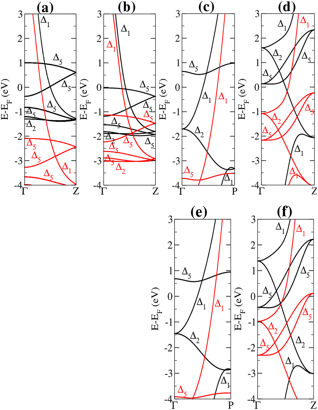 | ||
| Fig. 3 Real band structures of (a) hcp-Co, (b) hcp-Ni, (c) bcc-Co, and (d) bcc-Fe along the [0001], [0001], [111], and [001] directions, respectively. The majority spin bands are shown in red color and the minority spin bands are shown in black color. The Bloch state symmetry is indicated. Panels (e) and (f) show results analogous to panels (c) and (d), respectively, but without strain. | ||
C. Tunnel magnetoresistance
The momentum-dependence of the number of majority and minority spin transport channels at EF is addressed in Fig. 4. For hcp-Co (six-fold rotation symmetry) we find an increased concentration of majority spin transport channels in a circular region around the Γ-point, while the minority spin transport channels are spread across the entire BZ. For hcp-Ni (six-fold rotation symmetry) both the majority and minority spin transport channels are concentrated in a ring around the Γ-point. For bcc-Co (six-fold rotation symmetry) the majority and minority spin transport channels are concentrated inside and outside a circular region around the Γ-point, respectively. Finally, for bcc-Fe (four-fold rotation symmetry) increased concentrations of both majority and minority spin transport channels appear along the symmetry axes.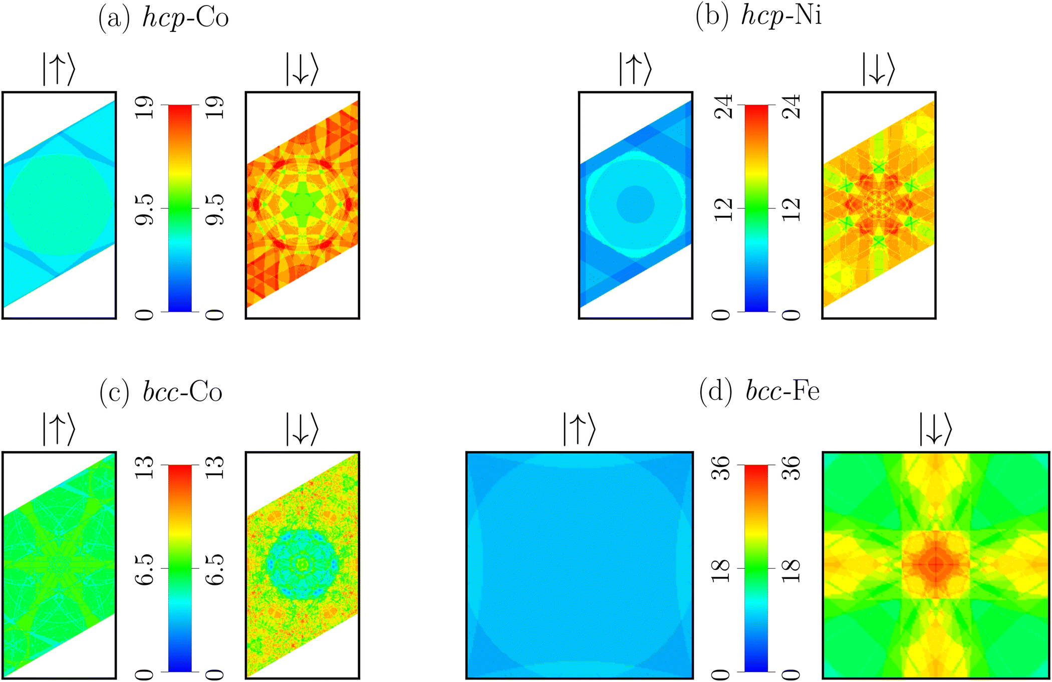 | ||
| Fig. 4 Momentum-dependence of the number of majority and minority spin transport channels (along the [0001], [0001], [111], and [001] directions, respectively) at EF in (a) hcp-Co, (b) hcp-Ni, (c) bcc-Co, and (d) bcc-Fe. The color range reaches up to the maximum of available transport channels. The results refer to simulation cells of 36 atoms. | ||
Fig. 5 shows the resultant TP(EF) and TAP(EF) in the BZ. For the Co/AlP/Co junction, TP(EF) is high in a broad circular region around the Γ-point in the spin majority channel and in narrow regions in the spin minority channel, while TAP(EF) is high only in narrow regions in both spin channels. For the Ni/AlP/Ni junction, both TP(EF) and TAP(EF) are high in circular regions around the Γ-point, and TAP(EF) is additionally high in circular regions close to the ends of the longer diagonal of the BZ in the spin minority channel. For the Co/GaN/Co junction, both TP(EF) and TAP(EF) are high in circular regions around the Γ-point in both spin channels. Finally, for the Fe/GaN/Fe junction, high values of both TP(EF) and TAP(EF) are found in large parts of the BZ in both spin channels.
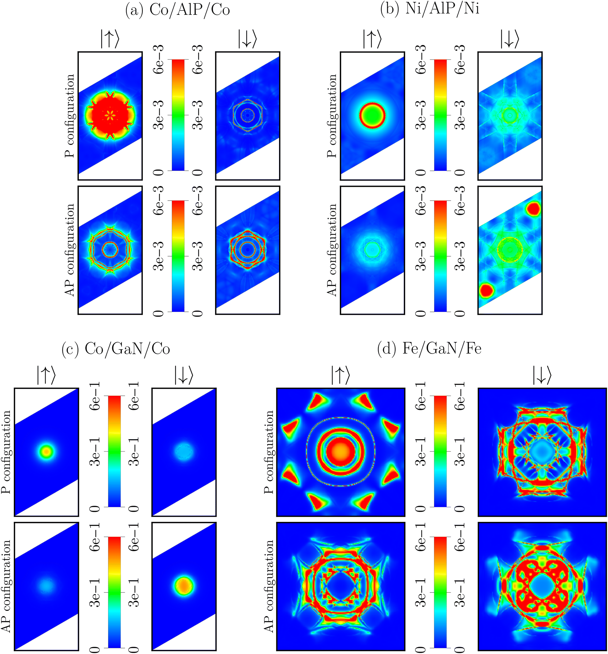 | ||
| Fig. 5 T P(EF) and TAP(EF) for the (a) Co/AlP/Co, (b) Ni/AlP/Ni, (c) Co/GaN/Co, and (d) Fe/GaN/Fe junctions. | ||
Fig. 6(a and b) shows for the AlP-based junctions that TP/AP(E) drops around EF by about three orders of magnitude. For the Co/AlP/Co junction, the majority spin channel contribution to TP(E) with Δ1 symmetry dominates over the minority spin channel contributions to TP(E) with Δ1 and Δ5 symmetries in the range −1 ≲ E − EF ≲ 0.5 eV and the minority spin channel contributions to TAP(E) with Δ1 and Δ5 symmetries dominate over the majority spin channel contribution to TAP(E) with Δ1 symmetry in the range 0 ≲ E − EF ≲ 1 eV. The low TAP(E) gives rise to a maximal TMR of ∼200% at EF. For the Ni/AlP/Ni junction, the minority spin channel contributions to TP(E) with Δ1 and Δ5 symmetries dominate over the majority spin channel contribution to TP(E) with Δ1 symmetry in the range −1 ≲ E − EF ≲ −0.5 eV and the minority spin channel contributions to TAP(E) with Δ1 and Δ5 symmetries dominate over the majority spin channel contribution to TAP(E) with Δ1 symmetry in the range −0.5 ≲ E − EF ≲ 0 eV, giving rise to a maximal TMR of ∼120% at E − EF = −0.8 eV.
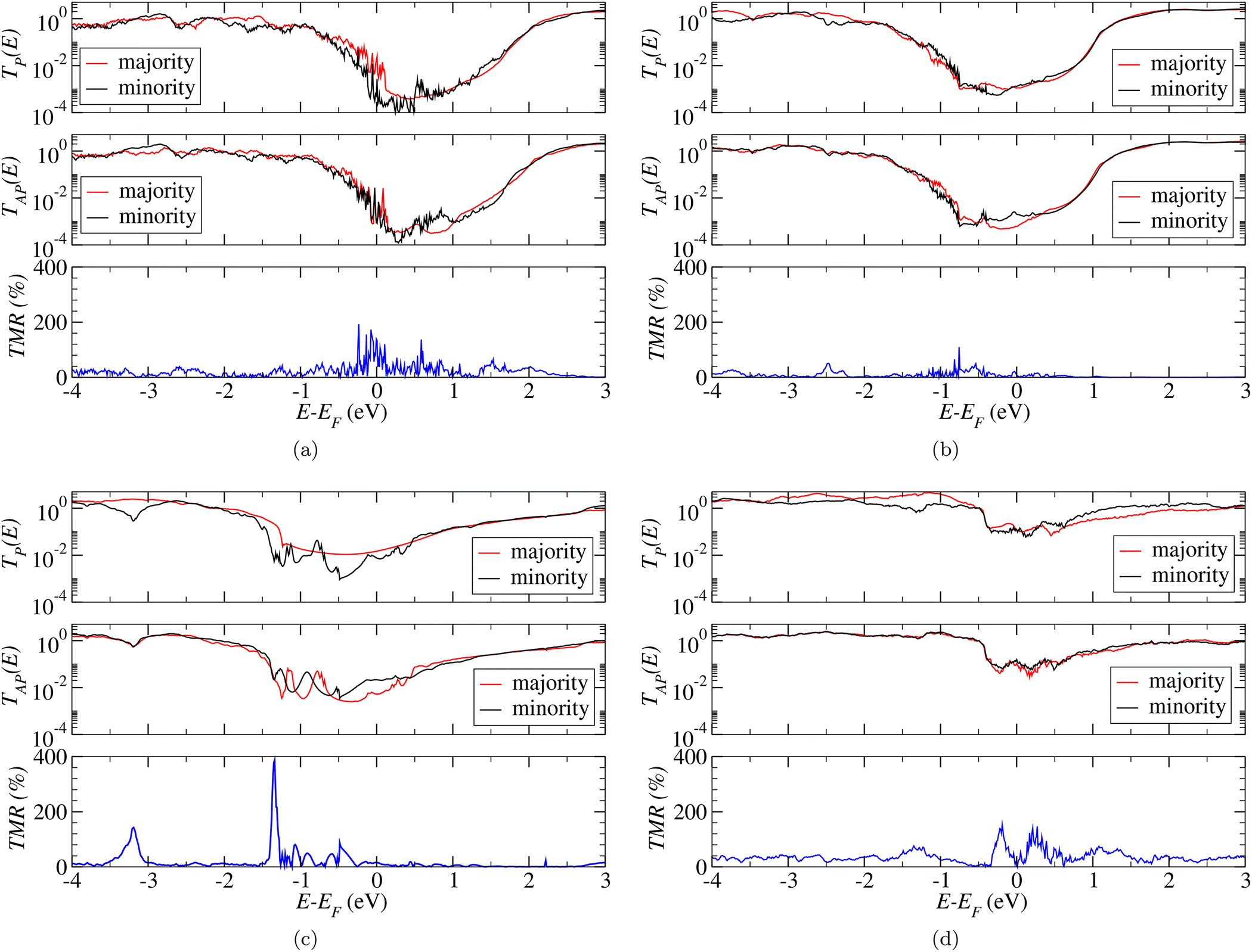 | ||
| Fig. 6 Transmission coefficients under P (top panels) and AP (middle panels) spin alignments of the electrodes as well as resultant zero bias TMR (bottom panels) as functions of the energy for the (a) Co/AlP/Co, (b) Ni/AlP/Ni, (c) Co/GaN/Co, and (d) Fe/GaN/Fe junctions. The AP spin alignment is obtained by flipping the spin direction in the right hand electrode. | ||
Fig. 6(c and d) shows for the GaN-based junctions that TP/AP(E) drops around EF by about two orders of magnitude. For the Co/GaN/Co junction, the majority spin channel contribution to TP(E) with Δ1 symmetry dominates over the minority spin channel contribution to TP(E) with Δ1 symmetry in the range −2 ≲ E − EF ≲ 1 eV and the minority spin channel contribution to TAP(E) with Δ1 symmetry dominates over the majority spin channel contribution TAP(E) with Δ1 symmetry in the range −0.5 ≲ E − EF ≲ 0.5 eV. The low TAP(E) gives rise to a maximal TMR of ∼300% at E − EF = −1.4 eV. For the Fe/GaN/Fe junction, the majority spin channel contributions to TP(E) with Δ2 and Δ5 symmetries dominate over the minority spin channel contributions to TP(E) with Δ1 and Δ2 symmetries in the range −3 ≲ E − EF ≲ −1 eV, the majority spin channel contributions to TP(E) with Δ1 and Δ5 symmetries dominate over the minority spin channel contributions to TP(E) with Δ2 and Δ5 symmetries in the range −1 ≲ E − EF ≲ 0 eV, and the minority spin channel contributions to TP(E) with Δ1 and Δ5 symmetries dominate over the majority spin channel contribution to TP(E) with Δ1 symmetry in the range 0 ≲ E − EF ≲ 2 eV. Moreover, the majority spin channel contributions to TAP(E) with Δ2 and Δ5 symmetries dominate over the minority spin channel contributions to TAP(E) with Δ1 and Δ2 symmetries in the range −3 ≲ E − EF ≲ −1 eV, the minority spin channel contributions to TAP(E) with Δ2 and Δ5 symmetries dominate over the majority spin channel contributions to TAP(E) with Δ1 and Δ5 symmetries in the range −1 ≲ E − EF ≲ 0 eV, the minority spin channel contributions to TAP(E) with Δ1, Δ2, and Δ5 symmetries dominate over the majority spin channel contribution to TAP(E) with Δ1 symmetry in the range 0 ≲ E − EF ≲ 2 eV, and the majority spin channel contribution to TAP(E) with Δ1 symmetry dominates over the minority spin channel contribution to TAP(E) with Δ1 symmetry in the range 2 ≲ E − EF ≲ 3 eV. As a result, we obtain a maximal TMR of ∼150% at both E − EF = −0.2 and 0.3 eV.
IV. Conclusion
We have explored the possibility of using the optoelectronic materials AlP and GaN as tunnel barriers in the next generation of magnetic tunnel junctions, which would enable the design of hybrid memory/logic components and spin-based displays. As ferromagnetic electrodes, we have considered hcp-Co, hcp-Ni, bcc-Co, and bcc-Fe. Analysis of the complex wave vectors of AlP and GaN has enabled us to establish the high transmission regions of the BZ and analysis of the complex band structures has provided us with the symmetries of the Bloch states dominating the transmission. For both semiconductors, both the valence band edge (dominated by pz orbitals) and the conduction band edge (dominated by s orbitals) are located at the Γ-point. The transmission probability turns out to be high for Bloch states of Δ1 symmetry. The Co/AlP/Co, Ni/AlP/Ni, Co/GaN/Co, and Fe/GaN/Fe junctions achieve at zero bias maximal TMRs of ∼200% (at EF), ∼120% (at E − EF = −0.8 eV), ∼300% (at E − EF = −1.4 eV), and ∼150% (at E − EF = −0.2 and 0.3 eV), respectively, which demonstrates that they are viable candidates particularly for low power applications.Conflicts of interest
There are no conflicts to declare.Acknowledgements
The research reported in this publication was supported by funding from King Abdullah University of Science and Technology.References
- Magnetoresistance in metals, ed. A. B. Pippard, Cambridge University Press, Cambridge, 1989 Search PubMed.
- M. Julliere, Tunneling between ferromagnetic films, Phys. Lett. A, 1975, 54, 225 CrossRef.
- M. N. Baibich, J. M. Broto, A. Fert, F. N. Van Dau, F. Petroff, P. Eitene, G. Greuzet, A. Friederich and J. Chazelas, Giant magnetoresistance of (001)Fe/(001)Cr magnetic superlattices, Phys. Rev. Lett., 1988, 64, 2472 CrossRef PubMed.
- G. Binasch, P. Grünberg, F. Saurenbach and W. Zinn, Enhanced magnetoresistance in layered magnetic structures with antiferromagnetic interlayer exchange, Phys. Rev. B: Condens. Matter Mater. Phys., 1989, 39, 4828 CrossRef CAS PubMed.
- F. J. Gregg, I. Petej, E. Jouguelet and C. Dennis, Spin electronics – A review, J. Phys. D: Appl. Phys., 2002, 35, R121 CrossRef.
- T. Miyazaki, N. Tezuka and S. Kumagai, Spin-polarized tunneling magnetoresistive effect in ferromagnet/insulator/ferromagnet junctions, Physica B Condens. Matter, 1997, 237–238, 256 CrossRef CAS.
- J. S. Moodera, L. R. Kinder, T. M. Wong and R. Meservey, Large magnetoresistance at room temperature in ferromagnetic thin film tunnel junctions, Phys. Rev. Lett., 1995, 74, 3273 CrossRef CAS PubMed.
- I. I. Mazin, How to define and calculate the degree of spin polarization in ferromagnets, Phys. Rev. Lett., 1999, 83, 1427 CrossRef CAS.
- W. H. Butler, X. G. Zhang, T. C. Schulthess and J. M. Maclaren, Spin-dependent tunneling conductance of Fe/MgO/Fe sandwiches, Phys. Rev. B: Condens. Matter Mater. Phys., 2001, 63, 054416 CrossRef.
- J. Mathon and A. Umerski, Theory of tunneling magnetoresistance of an epitaxial Fe/MgO/Fe(001) junction, Phys. Rev. B: Condens. Matter Mater. Phys., 2001, 63, 220403 CrossRef.
- S. S. P. Parkin, C. Kaiser, A. Panchula, P. M. Rice, B. Hughes, M. Samant and S. H. Yang, Giant tunnelling magnetoresistance at room temperature with MgO (100) tunnel barriers, Nat. Mater., 2004, 3, 862 CrossRef CAS PubMed.
- S. Yuasa, T. Nagahama, A. Fukushima, Y. Suzuki and K. Ando, Nat. Mater., 2004, 3, 868 CrossRef CAS PubMed.
- L. Berger, Emission of spin waves by a magnetic multilayer traversed by a current, Phys. Rev. B: Condens. Matter Mater. Phys., 1996, 54, 9353 CrossRef CAS PubMed.
- D. C. Ralph and M. D. Stiles, Spin transfer torques, J. Magn. Magn. Mater., 2008, 320, 1190 CrossRef CAS.
- S. I. Kiselev, J. C. Sankey, I. N. Krivorotov, N. C. Emley, R. J. Schoelkopf, R. A. Buhrman and D. C. Ralph, Microwave oscillations of a nanomagnet driven by a spin polarized current, Nature, 2003, 425, 380 CrossRef CAS PubMed.
- H. Meng, G. J. Wang and J. P. Wang, A spintronics full adder for magnetic CPU, IEEE Electron Device Lett., 2005, 26, 360 Search PubMed.
- W. Zhao, E. Belhaire and C. Chappert, Spin-MTJ based non-volatile flip-flop, Proceedings of the 7th IEEE Conference on Nanotechnology, Hong Kong, China, 2007, pp. 399.
- L. Montesi, Z. Zilic, T. Hanyu and D. Suzuki, Building blocks to use in innovative non-volatile FPGA architecture based on MTJs, Proceedings of the 2012 IEEE Computer Society Annual Symposium on VLSI, Amherst, USA, 2012, pp. 302.
- S. A. Iyengar, S. Ghosh and J. Jang, MTJ-based state retentive flip-flop with enhanced-scan capability to sustain sudden power failure, IEEE Trans. Circuits Syst. Regul. Pap., 2015, 62, 2062 Search PubMed.
- H. Cai, Y. Wang, L. Alves De Barros Naviner and W. Zhao, Low power magnetic flip-flop optimization with FDSOI technology boost, IEEE Trans. Magn., 2016, 52, 3401807 Search PubMed.
- J. S. Friedman and A. V. Sahakian, Complementary magnetic tunnel junction logic, IEEE Trans. Electron Devices, 2014, 61, 1207 Search PubMed.
- Y. Jiang, Y. Lv, M. Jamali and J. Wang, Spin analog-to-digital converter using magnetic tunnel junction and spin Hall effect, IEEE Electron Device Lett., 2015, 36, 511 Search PubMed.
- F. A. Vincent, J. Larroque, N. Locatelli, N. R. Ben, O. Bichler, C. Gamrat, S. W. Zhao, J. Klein, S. R. Galdin and D. Querlioz, Spin-transfer torque magnetic memory as a stochastic memristive synapse for neuromorphic systems, IEEE Trans. Biomed. Circuits Syst., 2015, 9, 166 Search PubMed.
- G. Srinivasan, A. Sengupta and K. Roy, Magnetic tunnel junction based long-term short-term stochastic synapse for a spiking neural network with on-chip STDP learning, Sci. Rep., 2016, 6, 29545 CrossRef CAS PubMed.
- J. Toreejon, M. Riou, F. A. Arauujo, S. Tsunegi, G. Khalsa, D. Querlioz, P. Bortolotti, V. Cros, K. Yakushiji, A. Fukushima, H. Kubota, S. Yuasa, M. D. Stiles and J. Grollier, Neuromorphic computing with nanoscale spintronic oscillators, Nature, 2017, 547, 428 CrossRef PubMed.
- H. Cai, H. Y. Wang, L. Alves De Barros Naviner and W. Zhao, Robust ultra-low power non-volatile logic-in-memory circuits in FD-SOI technology, IEEE Trans. Circuits Syst. Regul. Pap., 2017, 64, 847 Search PubMed.
- S. Bhatti, R. Sbiaa, A. Hirohata, H. Ohno, S. Fukami and S. N. Piramanayagam, Spintronics based random access memory: A review, Mater. Today, 2017, 20, 530 CrossRef.
- H. Lee, C. Grezes, A. Lee, F. Ebrahimi, P. A. Khalili and L. K. Wang, A spintronic voltage-controlled stochastic oscillator for event-driven random sampling, IEEE Electron Device Lett., 2017, 38, 281 Search PubMed.
- A. Sengupta, M. C. Liyanagedera, B. Jung and K. Roy, Magnetic tunnel junction as an on-chip temperature sensor, Sci. Rep., 2017, 7, 11764 CrossRef.
- K. Fujiwara, M. Oogane, A. Kanno, M. Imada, J. Jono, T. Terauchi, T. Okuno, Y. Aritomi, M. Morikawa, M. Tsuchida, N. Nakasato and Y. Ando, Magnetocardigraphy and magnetoencephalography measurements at room temperature using tunnel magneto-resistance sensors, Appl. Phys. Express, 2018, 11, 023001 CrossRef.
- I. Chakraborty, A. Agrawal and K. Roy, Design of a low-voltage analog-to-digital converter using voltage-controlled stochastic switching of low barrier nanomagnets, IEEE Magn. Lett., 2018, 9, 3103905 Search PubMed.
- S. Salehi, B. M. Mashhadi, A. Zaeemzadeh, N. Rahnavard and F. R. DeMara, Energy-aware adaptive rate and resolution sampling of spectrally sparse signals leveraging VCMA-MTJ devices, IEEE J. Emerging Sel. Top. Circuits Syst., 2018, 8, 679 Search PubMed.
- S. Salehi and F. R. DeMara, SLIM-ADC: Spin-based logic-in-memory analog to digital converter leveraging SHE-enabled domain wall motion devices, Microelectron. J., 2018, 81, 137 CrossRef.
- Z. Wang, L. Zhang, M. Wang, Z. Wang, D. Zhu, Y. Zhang and W. Zhao, High-density NAND-like spin transfer torque memory with spin orbit torque erase operation, IEEE Electron Device Lett., 2018, 39, 343 CAS.
- K. Garello, F. Yasin and S. G. Kar, Spin-orbit torque MRAM for ultrafast embedded memories: From fundamentals to large scale technology integration. Proceedings of the 11th IEEE International Memory Workshop, Monterey, USA, 2019.
- C. E. Marques, N. Maciel, L. Naviner, H. Cai and J. Yang, A review of sparse recovery algorithms, IEEE Access, 2019, 7, 1300 Search PubMed.
- J. Kaiser, W. A. Borders, K. Y. Camsari, S. Fukami, H. Ohno and S. Datta, Hardware-aware in situ Boltzmann machine learning using stochastic magnetic tunnel junctions, Phys. Rev. Appl., 2022, 17, 014016 CrossRef CAS.
- H. X. Liu, Y. Honda, T. Taira, K. I. Matsuda, M. Arita, T. Uemura and M. Yamamoto, Giant tunneling magnetoresistance in epitaxial Co2MnSi/MgO/Co2MnSi magnetic tunnel junctions by half-metallicity of Co2MnSi and coherent tunneling, Appl. Phys. Lett., 2012, 101, 132418 CrossRef.
- N. M. Caffrey, T. Archer, I. Rungger and S. Sanvito, Coexistance of giant tunneling electroresistance and magnetoresistance in an all-oxide composite magnetic tunnel junction, Phys. Rev. Lett., 2012, 109, 226803 CrossRef PubMed.
- N. Jutong, I. Rungger, C. Schuster, U. Eckern, S. Sanvito and U. Schwingenschlögl, Electronic transport through EuO spin-filter tunnel junctions, Phys. Rev. B: Condens. Matter Mater. Phys., 2012, 86, 205310 CrossRef.
- S. V. Faleev, S. S. P. Parkin and O. N. Mryasov, Brillouin zone spin filtering mechanism of enhanced tunneling magnetoresistance and correlation effects in a Co(0001)/h-BN/Co(0001) magnetic tunnel junction, Phys. Rev. B: Condens. Matter Mater. Phys., 2015, 92, 235118 CrossRef.
- G. Shukla, T. Archer and S. Sanvito, HfO2 and SiO2 as barriers in magnetic tunneling junctions, Phys. Rev. B, 2017, 95, 184410 CrossRef.
- R. Stearrett, W. G. Wang, X. Kou, J. F. Feng, J. M. D. Coey, J. Q. Xiao and E. R. Nowak, Influence of exchange bias on magnetic losses in CoFeB/MgO/CoFeB tunnel junctions, Phys. Rev. B: Condens. Matter Mater. Phys., 2012, 86, 014415 CrossRef.
- S. M. Bhagat and P. Lubitz, Temperature variation of ferromagnetic relaxation in the 3d transition metals, Phys. Rev. B: Solid State, 1974, 10, 179 CrossRef CAS.
- R. Fiederling, M. Keim, G. Reuscher, W. Ossau, G. Schmidt, A. Waag and L. W. Molenkamp, Injection and detection of a spin polarized current in a light-emitting diode, Nature, 1999, 402, 787 CrossRef.
- J. R. Schaibley, H. Yu, G. Clark, P. Rivera, J. S. Ross, K. L. Seyler, W. Yao and X. Xu, Valleytronics in 2D materials, Nature, 1999, 402, 787 CrossRef.
- D. M. Ceperley and B. J. Alder, Ground state of the electron gas by a stochastic method, Phys. Rev. Lett., 1980, 45, 566 CrossRef CAS.
- N. Troullier and J. L. Martins, Efficient pseudopotentials for plane-wave calculations, Phys. Rev. B: Condens. Matter Mater. Phys., 1991, 43, 1993 CrossRef CAS PubMed.
- C. D. Pemmaraju, T. Archer, D. Sánchez-Portal and S. Sanvito, Atomic-orbital-based approximate self-interaction correction scheme for molecules and solids, Phys. Rev. B: Condens. Matter Mater. Phys., 2007, 75, 045101 CrossRef.
- A. Filippetti, C. D. Pemmaraju, S. Sanvito, P. Delugas, D. Puggioni and V. Fiorentini, Variational pseudo-self-interaction-corrected density functional approach to the ab initio description of correlated solids and molecules, Phys. Rev. B: Condens. Matter Mater. Phys., 2011, f84, 195127 CrossRef.
- E. A. Owen and D. M. Jones, Effect of grain size on the crystal structure of cobalt, Proc. Phys. Soc. B, 1954, 67, 456 CrossRef.
- V. Darakchieva, B. Monemar and A. Usui, On the lattice parameters of GaN, Appl. Phys. Lett., 2007, 91, 031911 CrossRef.
- Y. I. Petrov, E. A. Shafranovsky, Y. F. Krupyanskii and S. V. Essine, Structure and Mössbauer spectra for the Fe-Cr system: From bulk alloy to nanoparticles, J. Appl. Phys., 2002, 91, 352 CrossRef CAS.
- X. H. Zheng, Y. T. Wang, Z. H. Feng, H. Yang, H. Chen, J. M. Zhou and J. W. Liang, Method for measurement of lattice parameter of cubic GaN layers on GaAs (001), J. Cryst. Growth, 2003, 250, 345 CrossRef CAS.
- A. R. Rocha, V. M. Garcia Suarez, S. Bailey, C. J. Lambert, J. Ferrer and S. Sanvito, Towards molecular spintronics, Nat. Mater., 2005, 4, 335 CrossRef CAS PubMed.
- A. R. Rocha, V. M. Garcia-Suarez, S. Bailey, C. J. Lambert, J. Ferrer and S. Sanvito, Spin and molecular electronics in atomically generated orbital landscapes, Phys. Rev. B: Condens. Matter Mater. Phys., 2006, 73, 085414 CrossRef.
- I. Rungger and S. Sanvito, Algorithm for the construction of self-energies for electronic transport calculations based on singularity elimination and singular value decomposition, Phys. Rev. B: Condens. Matter Mater. Phys., 2008, 78, 035407 CrossRef.
- H. Cui, Y. Zhang, Q. Kang, H. M. Chang, X. B. Zhang, R. H. Zhai and G. Q. Wang, Bandgaps properties of III-phosphides (BP, AlP, GaP, InP) materials excited by ultrasonic, Optik, 2019, 177, 58 CrossRef CAS.
- P. Rinke, A. Qteish, J. Neugebauer, C. Freysoldt and M. Scheffler, Combining GW calculations with exact-exchange density-functional theory: An analysis of valence-band photoemission for compound semiconductors, New J. Phys., 2005, 7, 126 CrossRef.
- F. Sacconi, J. M. Jancu, M. Povolotskyi and A. Di Carlo, Full-band tunneling in high-κ oxide MOS structures, IEEE Trans. Electron Devices, 2007, 54, 3168 CAS.
| This journal is © The Royal Society of Chemistry 2023 |