
Impedance spectroscopy of Sb2Se3 photovoltaics consisting of (Sb4Se6)n nanoribbons under light illumination†
Jaemin
Park‡
a,
Thomas P.
Shalvey‡
b,
Thomas
Moehl
c,
Kyoohee
Woo
 d,
Jonathan D.
Major
b,
S. David
Tilley
c and
Wooseok
Yang
*ae
d,
Jonathan D.
Major
b,
S. David
Tilley
c and
Wooseok
Yang
*ae
aSchool of Chemical Engineering, Sungkyunkwan University (SKKU), 16419, Republic of Korea. E-mail: wooseok.yang@skku.edu
bStephenson Institute for Renewable Energy, Physics Department, University of Liverpool, Liverpool L69 7ZF, UK
cDepartment of Chemistry, University of Zurich, Winterthurerstrasse 190, 8057 Zurich, Switzerland
dDepartment of Printed Electronics, Korea Institute of Machinery & Materials, Daejeon 305-343, South Korea
eSKKU Institute of Energy Science and Technology (SIEST), Sungkyunkwan University, Suwon 16419, Republic of Korea
First published on 29th November 2023
Abstract
Sb2Se3, consisting of one-dimensional (Sb4Se6)n nanoribbons has drawn attention as an intriguing light absorber from the photovoltaics (PVs) research community. However, further research is required on the performance-limiting factors in Sb2Se3 PVs. In this study, we investigated the charge carrier behavior in Sb2Se3 PVs by impedance spectroscopy (IS) under light illumination. (Sb4Se6)n nanoribbons with two different orientations were used to investigate the effect of crystal orientation on the device performance. Regardless of the (Sb4Se6)n orientation, negative capacitance was observed at forward bias, representing a recombination pathway at the TiO2/Sb2Se3 interface. A comparison of the recombination resistances and lifetimes of two different Sb2Se3 PVs showed that a better interface could be formed by placing the (Sb4Se6)n ribbons parallel to the TiO2 layer. Based on these observations, an ideal structure of the Sb2Se3/TiO2 interface is proposed, which will enhance the performance of Sb2Se3 PVs toward its theoretical limit.
 Wooseok Yang | Prof. Wooseok Yang is an Assistant Professor at the School of Chemical Engineering at Sungkyunkwan University (SKKU) in Korea. He received his BS in 2012 from the Department of Ceramic Engineering and his PhD in 2018 from the Department of Materials Science and Engineering at Yonsei University in Korea. From 2019 to 2021, he worked as a postdoctoral researcher at the University of Zurich in Switzerland with Prof. David Tilley before joining SKKU in 2022. His research focuses on (photo-)electrochemical energy conversion, such as photoelectrochemical water splitting, electrochemical CO2 capture, and valorization of waste biomass. |
1. Introduction
Antimony selenide (Sb2Se3), owing to its unique properties, has recently captured considerable attention as a semiconductor material in thin-film photovoltaics (PVs). In addition to its inexpensive cost and simple composition, the fundamental properties of Sb2Se3, such as its band gap, light absorption coefficient, and mobilities, demonstrate the material's potential as a promising light absorber. The more intriguing nature of Sb2Se3 is its one-dimensional (1D) crystal structure comprising (Sb4Se6)n nanoribbons packed with weak van der Waals forces. The formation of nanoribbons can be predicted through first-principles simulations. Computational calculations indicate that the surface energies for the (hk0) surfaces are lower than (hk1).1 This suggests that the most prevalent surfaces in Sb2Se3 samples will be the (hk0) surfaces, which are parallel to the [001] direction, leading to the formation of nanoribbons. When the ribbons are placed parallel to the grain boundary (GB), contrary to other semiconductors in which the GBs are detrimental to the performance, the GB of Sb2Se3 is known to be electrically benign.1 Moreover, atomic relaxation—the so-called “self-healing” process—removes the deep trap states within the band gap of Sb2Se3 not only at the GBs but also at all crystallographic orientations of Sb2Se3.2 Owing to these interesting characteristics, efforts have been devoted to fabricate Sb2Se3-based high-performance devices in the solar cell3 and water splitting4 fields. Despite their increasing efficiencies, it is necessary to further enhance their performance, which requires deeper understanding of the performance-limiting factors.Impedance spectroscopy (IS) is a powerful characterization technique for optoelectronic devices. Its value lies in its ability to separate the contributions of different layers or regions of the device from the performance of the overall device.5 For instance, by analyzing frequency-based current–voltage responses with small amplitudes, IS can individually extract information such as resistances, capacitances, and time constants from each of the device regions.6 This comprehensive understanding can provide valuable insights for optimizing and improving the performance of various devices by identifying the performance-limiting sources. Consequently, the IS technique has been applied to various materials systems and devices, including (dye-sensitized) solar cells,7,8 water-splitting devices,9 batteries,10 fuel cells,11 and sensors.12
IS measurement is also widely used by the thin-film solar cells community to demonstrate various photo-physical processes. For instance, in halide perovskite-based solar cells, several models and mechanisms have been established, including charge transfer, recombination-related resistance and capacitance, and the presence of negative capacitance.13,14 However, systematic studies using IS of Sb2Se3 solar cells have not yet been reported. Most existing research have performed only limited comparisons among samples, while comprehensive exploration of IS data under various light and voltage conditions remains elusive.15–19 Notably, the crystallographic orientation of the Sb2Se3 thin film has a pivotal role in the solar cell performance because of its anisotropic properties.1 Electron mobility and GB characteristics can be altered by changing the orientation of the stacked 1D (Sb4Se6)n nanoribbons in Sb2Se3 film, which inevitably affects the device efficiencies.20 Therefore, IS characterization of Sb2Se3-based solar cells, including the TiO2-electron transport layers (ETL) with Sb2Se3 having different crystallographic orientations, is significantly important as it forms the fundamental basis for improving the overall performance of the device.
In this study, we first present the result of the in-depth IS characterization of Sb2Se3 solar cells. By examining the information obtained from analyzing the IS data of TiO2-ETL Sb2Se3 solar cells, we attained insights about the semiconductor and TiO2/Sb2Se3 interfaces, such as the recombination processes, lifetimes of carriers, and flat band potentials under different light intensities, and applied potentials. In addition, ‘negative capacitance’ was observed in Sb2Se3 solar cells; therefore, a recombination-related mechanism was proposed for the first time to explain this phenomenon. Furthermore, IS data was carefully investigated according to the crystallographic orientations, i.e., the orientation of (Sb4Se6)n nanoribbons. More favorable interface characteristics, a larger recombination resistance, and a longer lifetime were observed when the (Sb4Se6) ribbons were parallel to the TiO2 layer. Based on these findings, we have proposed a novel Sb2Se3 solar-cell configuration that shows promising potential for future advancements and development. Our results reveal the effectiveness of the IS technique in identifying the performance-limiting factors under operational conditions, paving the way for advancements of Sb2Se3-based solar cells.
2. Results and discussion
The compact film-type Sb2Se3-film-based PV with [hk1] oriented crystallographic orientation achieved higher efficiencies than the [hk0]-oriented devices because the carrier transport in Sb2Se3 along the [001] direction was more efficient than that along the other directions owing to its anisotropic crystallographic nature.1 A two-step close space sublimation (CSS) method was employed to avoid the formation of the thermodynamically favorable 1D structure and the rearrangement of (Sb4Se6)n nanoribbons along the [hk1] direction.21 A thin seed layer was pre-deposited at a relatively low substrate temperature (350 °C), which then recrystallized during the higher-temperature (450 °C) main growth step.22Fig. 1a depicts the microstructures of compact Sb2Se3 thin films deposited on fluorine-doped tin oxide (FTO) substrate with a TiO2-ETL by a two-step CSS deposition process. The cross-section scanning electron microscope (SEM) image of the corresponding Sb2Se3 film is presented in Fig. S1 (ESI†). The experimental details are described in the Experimental section. The orientation of the crystal can be anticipated by measuring the crystallographic planes, since the nanoribbons act as a fundamental building block of the Sb2Se3 structure if this basic repeat unit is not broken. In this regard, most of the literature used X-ray diffraction (XRD) analysis to predict the crystallographic orientation of the Sb2Se3 film. These findings align closely with the results obtained from the direct measurement of the orientation of (Sb4Se6)n ribbons through TEM imaging.1,23 The crystallographic orientations of the Sb2Se3 film were investigated by XRD analysis (Fig. 1b). The sample showed diffraction patterns corresponding to orthorhombic Sb2Se3 (Joint Committee on Powder Diffraction Standards, JCPDS 15-0861, space group Pbnm). In addition, the dominant [211] and [221] orientations of Sb2Se3 in the XRD patterns (Fig. 1c) confirm the success of the seed-derived growth strategy for preferred [hk1]-oriented film growth by using a kinetically controlled growth.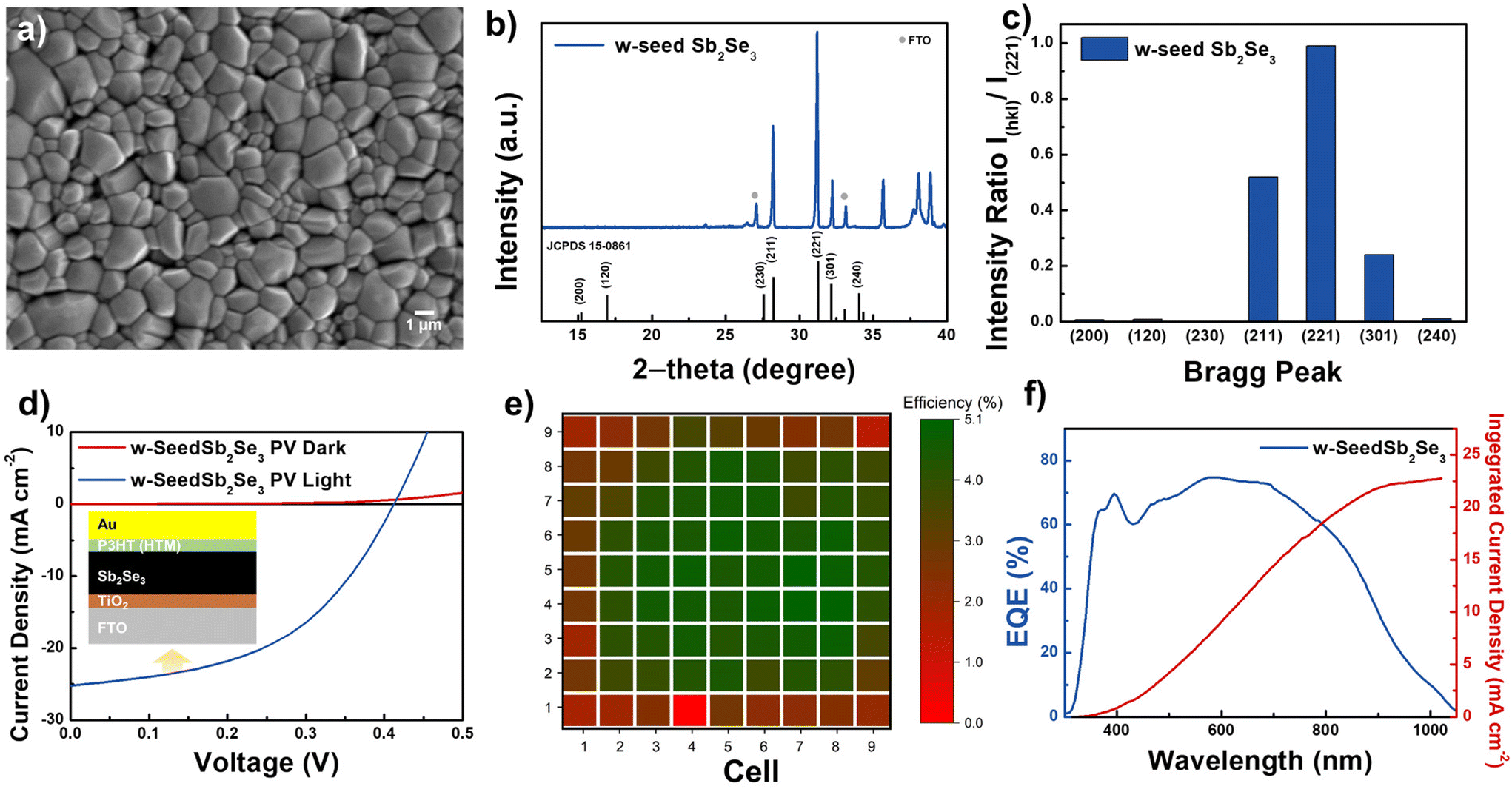 | ||
| Fig. 1 (a) Top-view SEM images of the w-seed Sb2Se3 films. (b) Diffraction patterns and (c) peak intensities ratio (I(hkl)/I(221)) of the obtained Sb2Se3 films. (d) J–V characteristics of champion Sb2Se3 PV. (e) 2D plot of the PCE values of the large area Sb2Se3 PV (25 cm2) for each sub cell. (f) External quantum efficiency (EQE) spectra of a w-seed Sb2Se3-based PV. | ||
Sb2Se3 PV devices were fabricated using Sb2Se3 film, a poly(3-hexylthiophene) (P3HT) hole transfer layer (HTL), and Au electrode (denoted w-seed Sb2Se3 PV, inset of Fig. 1d). Fig. 1d displays representative current density–voltage (J–V) curves of the Sb2Se3 PV. Typical J–V characterizations performed under 1 sun illumination yielded an optimal conversion efficiency of 5.01% for the Sb2Se3 PV with an open circuit voltage (VOC) of 0.41 V, short circuit current density (JSC) of 25.20 mA cm−2, and fill factor (FF) of 47.96%. To provide statistical information on the device performance, 81 individual devices in a 5 × 5 cm2 FTO glass were fabricated (Fig. S2, ESI†). To finalize fabrication of the subcells, HTL/Au layers were deposited on them. With optimal depositing condition, we achieved an average VOC of 0.40 ± 0.05 V, JSC of 20.53 ± 3.67 mA cm−2, and FF of 43.53 ± 6.48% from the 81 subcells (Fig. S3, ESI†), indicating the high uniformity of the device parameters in the w-seed Sb2Se3 PVs, except for the edges, which are more prone to pinholes (Fig. 1e). Measurement of the external quantum efficiency (EQE) showed that the photocurrent contribution extended to over 1000 nm, which was consistent with the measured optical bandgap.20 In addition, the photocurrent calculated by integrating the EQE over the light spectrum was nearly identical to the values determined via J–V characterizations.
IS analysis was performed with the w-seed Sb2Se3 PVs under white LED light illumination as a function of the applied potential. Fig. 2a shows the current density with 10% sun white LED, which was calibrated with a Si diode. It should be noted that the current density is not exactly 10% of the value measured under 1 sun illumination with the Xe lamp (Fig. 1d), owing to differences in the wavelength-dependent absorption of the Si diode and Sb2Se3. Fig. 2b–d show the Nyquist plots at each applied potential. When the applied potential was more positive than the VOC (∼0.32 V), an inductive response, which is mathematically equivalent to a “negative capacitance”, was observed at the very low frequency region (Fig. 2b, inset c). Considering the definition of capacitance (C), C = dQ/dV, a negative capacitance would mean a decreased charge (Q) when the applied voltage (V) is increased. This negative capacitance was observed in organic PV24 and hybrid perovskite PV14 devices. Mora-Sero et al. reported a negative capacitance in an inorganic CdSe-based device, which is not observed in a conventional monocrystalline Si solar cell.25 They attributed the negative capacitance to an additional recombination pathway that opens up at forward bias and decreases the charge accumulation ability of the solar cells. It was also reported that a negative capacitance can originate from a time-dependent trap-assisted recombination process.26 Note that a possible trap-mediated recombination process was proposed at the Sb2Se3/TiO2 interface in the previous IS study on Sb2Se3 photocathode for photoelectrochemical water splitting.9 Thus, the recombination at the Sb2Se3/TiO2 interface, which is activated at forward bias, could be one source of the negative capacitance. The photo-shunt, observed as the crossing point between dark and photocurrents after passing the VOC (Fig. 1d), indicates activation of an additional recombination pathway in the PV device at forward bias.
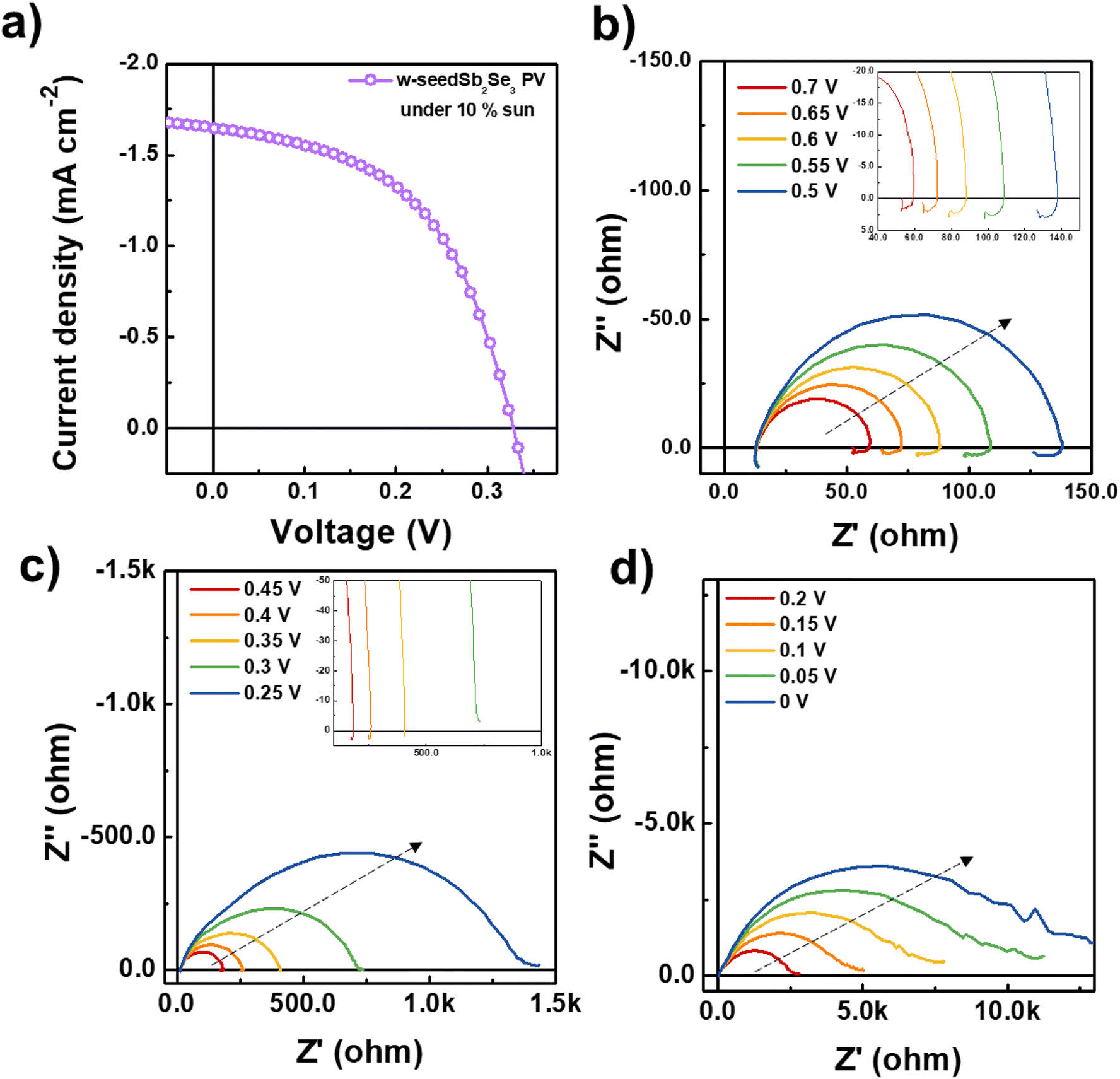 | ||
| Fig. 2 (a) J–V curve of the w-seed Sb2Se3 PV under 10% sun illumination. (b–d) Nyquist plots of the w-seed Sb2Se3 PV at the designated applied potential. | ||
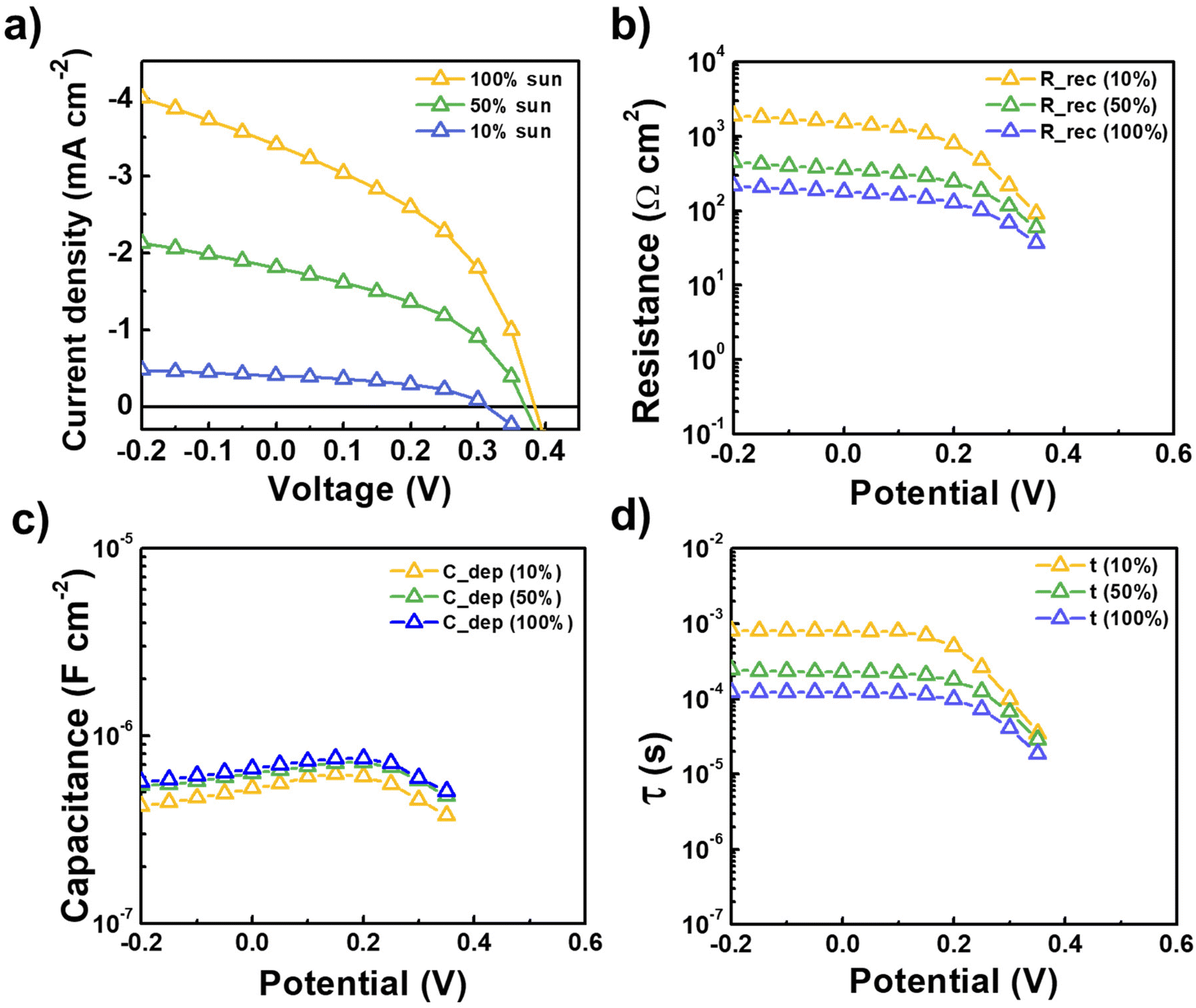
Another evident feature in the IS spectra of the Sb2Se3 PVs is the increasing size of the semicircle as the applied potential approaches the short circuit (Fig. 2b–d). The fact that higher resistance was observed at higher photocurrent regions implies that the resistance originates from a recombination process. In order to elucidate the nature of this resistance, IS spectra with higher light intensities were measured. Fig. 3a shows the current densities with 10, 50, and 100% sun LED light illumination. A small semicircle was observed at higher light intensities, indicating decreasing resistance as the light intensity increases (Fig. S4, ESI†). We fitted the Nyquist plots with the simple Voight circuit with three or two RC elements (Fig. S5, ESI†). The high frequency resistance, RHF, which is almost constant over potentials (Fig. S6†), is considered an artifact and not attributed to real physical phenomena, as we demonstrated in our previous study.9 Thus, we focused on the resistance, capacitance, and RC time constant from the low-frequency semicircle, as shown in Fig. 3b–d. As the low-frequency resistance is related to the recombination process, we denoted it as Rrec. The light intensity dependency indicates that the resistance to recombination decreases (i.e., the more chance to recombine) at a higher light intensity, providing further support that the resistance originates from the recombination process. The corresponding capacitance exhibited a different trend: a higher capacitance was observed in relation to the light intensity near the VOC region (Fig. 3c). The capacitance originated from the depletion region at the TiO2/Sb2Se3 interface, as evidenced by Mott–Schottky plots representing doping densities close to that of Sb2Se3 (Fig. S7 and ESI Note 1, ESI†). The higher doping density under higher light intensity may reflect the contribution of the photo-generated charges. The RC time constant can be obtained by multiplying the resistance and capacitance, as shown in Fig. 3d. The time constant, which represents the lifetime of the photo-generated charge carriers, was higher under lower light intensity, proving that faster recombination occurs when the population of the photo-generated carrier is high.
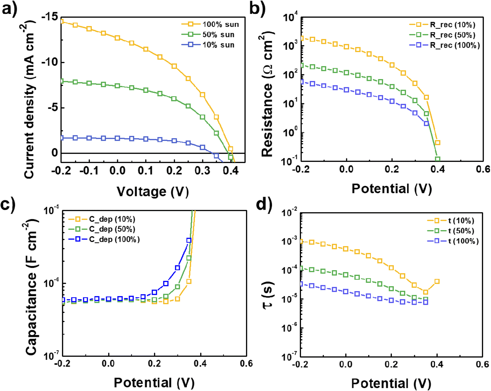 | ||
| Fig. 3 (a) Steady-state photocurrent densities obtained by the w-seed Sb2Se3 PV during IS measurement under 10%, 50%, and 100% sun illumination. (b) Resistances (c) capacitance, and (d) time constants for charge transfer of the w-seed Sb2Se3 PV from the IS fitting procedure. | ||
To investigate the carrier dynamics depending on the crystallographic orientation of the Sb2Se3 film, we prepared a reference Sb2Se3 film that was deposited quickly at lower substrate temperature and did not contain a seed layer (denoted w/o-seed Sb2Se3 film) for a comparative study. As shown in Fig. 4a and b, the values of the XRD peak intensities of the (hk0) planes/peak intensities of (221) planes were higher than those of the w-seed Sb2Se3 film, indicating that the more (Sb4Se6)n nanoribbons that grew along the [001] direction were horizontally laid on the superstrate. As shown in Fig. S8 and S9 (ESI†), attempts to use the w/o-seed Sb2Se3 film for PVs resulted in low efficiencies compared to the w-seed Sb2Se3 PV, especially for the photocurrent density. It seems that carriers are required to hop across (Sb4Se6) ribbons held by van der Waals forces in w/o-seed Sb2Se3 containing horizontally laid (Sb4Se6) ribbons. Moreover, as shown in the Fig. S10 (ESI†), the w/o-seed Sb2Se3 film contains more pin-holes than the w-seed Sb2Se3 film owing to its narrow thickness. The exposure of the superstrate can result in direct contact between the n-type TiO2 and p-type P3HT, which acts as a recombination center. Therefore, poor photocurrent arose from the recombination of the photogenerated charge carriers in the w/o-seed Sb2Se3 film, owing to its inefficient carrier-transport behavior and decreased shunt resistance. It is crucial to note that the deposition method for the w/o-seed Sb2Se3 film was also optimized in our previous study to achieve a planar film-type morphology aiming at attaining a planar film-type morphology.27 This optimization involved meticulous control of the source and substrate temperatures, preventing the formation of 1D structures. The resultant film demonstrated surface morphology and XRD patterns are determined by the source and substrate temperatures, while thickness is a separated parameter.27 As shown in Fig. 4c, current densities with 10% white light intensities were measured, and IS analysis was conducted with the w/o-seed Sb2Se3 PVs under 10% sun light illumination as a function of the applied potential (Fig. 4d–f). When the applied potential was more positive than the VOC (∼0.3 V), a similar propensity was exhibited that inductive negative capacitance was observed at the very low frequency region (Fig. 4d and e inset). Thus, it is believed that trap-mediated recombination at the Sb2Se3/TiO2 interface is also activated in w/o-seed Sb2Se3 at forward bias. Moreover, an increasing size of the main semicircle as the applied potential approached the short circuit was also observed in the IS spectra of the w/o-seed Sb2Se3 PVs, implying that the resistance originated from the recombination process, as in the w-seed Sb2Se3 PVs.
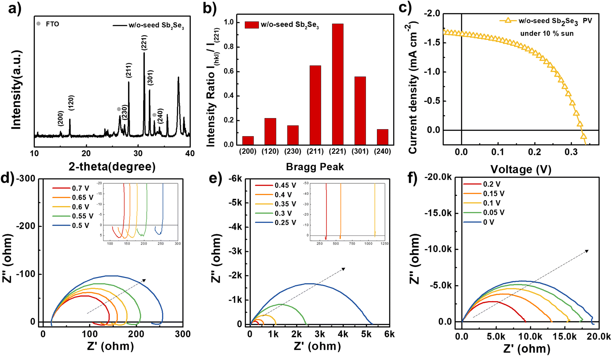 | ||
| Fig. 4 (a) Diffraction patterns and (b) peak intensities ratio (I(hkl)/I(221)) of the obtained w/o-seed Sb2Se3 films (c) J–V behavior exhibited by the w/o-seed Sb2Se3 PV under 10% sun illumination. (d–f) Nyquist plots of the w/o-seed Sb2Se3 PV at the designated applied potential. | ||
As shown in Fig. 5a, current densities with various LED light intensities were measured, and IS spectra with higher light intensities were measured for the w/o-seed Sb2Se3 PV. Increased resistance was observed as the applied potential moved toward the short circuit for all light conditions. Identical Voight circuits (Fig. S5†) were used to fit the Nyquist plots, and the resulting resistance, RC time constants, and capacitance are displayed in Fig. 5b–d, respectively. The resistance and time constant also decreased as the light intensity increased, which confirms that similar recombination-related mechanisms may exist in w/o-seed Sb2Se3 PVs. Divergent capacitance profiles are evident around the VOC in the two devices. However, the photo-physical processes significantly change near the VOC. Some R–C elements (e.g., negative capacitance) disappear while a new R–C element (e.g., depletion region and recombination) appears as the applied potential passes the VOC, making it challenging to fit and interpret the Nyquist plots. Thus, there can be some ambiguity and care must be taken to interpret the EIS data near this “transition condition”. In the VOC region, an observation of increasing capacitance with increasing applied voltage was observed for the w-seed Sb2Se3-based device. In contrast, the w/o-seed Sb2Se3-based device exhibited a lower capacitance that did not exhibit an increase. We have validated that this capacitance is associated with the depletion region through Mott–Schottky plots (Fig. S7 and ESI Note 1, ESI†). In an ideal semiconductor junction, an increase in applied voltage leads to a reduction in the depletion region and a consequent rise in capacitance originated from the depletion region (eqn (1) and (2))
 | (1) |
 | (2) |
 | ||
| Fig. 5 (a) Steady-state photocurrent densities of the w/o-seed Sb2Se3-based PV during IS measurement under 10%, 50%, and 100% sun illumination. (b) Resistances, (c) capacitance, and (d) time constants for the charge transfer of w/o-seed Sb2Se3 PV from the IS fitting procedure. | ||
A possible explanation for the longer lifetime in the w/o-seed Sb2Se3 sample is in its TiO2/Sb2Se3 interface. As the time constant can be obtained by multiplying the resistance and capacitance originating from the depletion region at the TiO2/Sb2Se3, it is reasonable to assume that the calculated time constant represents the lifetime of the photo-generated charge carriers at the TiO2/Sb2Se3 interfaces at the given applied potential. In the w/o-seed Sb2Se3 film, containing an (hk0) plane, the (Sb4Se6) ribbons lie parallel to the TiO2 layer. Hence, a high-quality Sb2Se3/TiO2 interface with Wan der Waals planes that has fewer trap sites can be formed. On the contrary, more recombination centers can be created at the interface of the w-seed Sb2Se3 film and TiO2 owing to the dangling bond at the (hk1) planes. As a result, the photo-generated carriers in the interfaces have a shorter lifetime, even though they are readily collected in a vertical direction within the covalently bonded (Sb4Se6) ribbons along the [001] direction within the Sb2Se3 film that only contains (hk1) planes. In other words, the interface of the w/o-seed Sb2Se3 film and TiO2 itself is superior, as the nanoribbons are combined with TiO2 horizontally. However, a lower performance is observed because of the decreased shunt resistance and severe bulk recombination derived from the pin-holes and inefficient charge transport due to the carrier hoping among the ribbons. The decreased shunt resistance of the w-seed Sb2Se3 PV is in accordance with the decreased dark current (Fig. S11†). Therefore, a bilayer structure is the most suitable.
A bilayer structure comprises a bottom thin layer of (Sb4Se6) ribbons arranged horizontally to the TiO2 layer and a top film with vertically aligned (Sb4Se6) ribbons. This design ensures efficient charge transport through covalent bonds and provides sufficient thickness to prevent pinholes. Such a configuration can effectively transport the charge carriers without recombination and also passivate the interface defect (Fig. 6). However, there will be an interface between the two layers, which can possibly affect the charge transport. The practical feasibility of having vertically aligned ribbons coexist with 100% parallel-oriented nanoribbons presents a significant challenge. Consequently, there is a notable likelihood of additional film growth within certain existing vertically aligned nanoribbons through the formation of new covalent bonds at dangling sites. Furthermore, the Sb2Se3/Sb2Se3 interface is anticipated to exhibit relative freedom from defects attributed to differences in lattice parameters. Therefore, we believe that this interface would have a comparatively lesser adverse impact on charge transport than the interface between Sb2Se3 and TiO2. Nevertheless, a more in-depth analysis is required to comprehend the implications of the additional interface and the improved Sb2Se3/TiO2 interface on performance once the device is implemented.
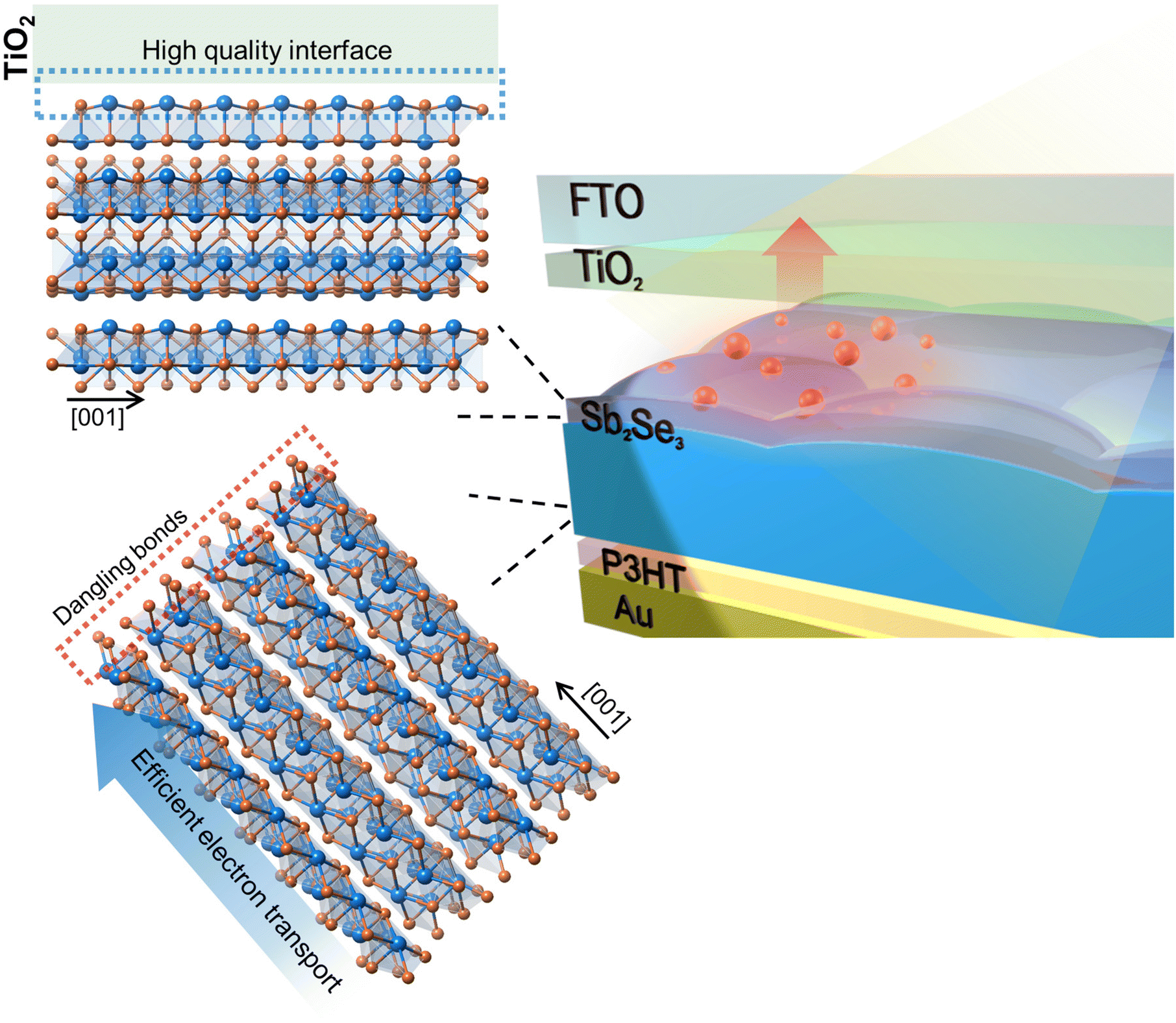 | ||
| Fig. 6 Schematic illustration of the proposed novel bilayer Sb2Se3 configuration that can effectively transport the charge carriers without recombination and also form a high quality interface with the TiO2 layer. | ||
3. Conclusions
In summary, we performed IS characterization of Sb2Se3 PVs with two different (Sb4Se6) ribbon orientations under illumination. The w-seed Sb2Se3, with the [hk1] orientations, exhibited a better uniformity and performance, particularly with regard to JSC and efficiency. Both samples exhibited negative capacitance behaviors at large forward bias, indicating that a trap mediated recombination pathway can be activated at the Sb2Se3/TiO2 interface regardless of the crystallographic orientation. Additionally, both samples exhibited a recombination-related resistance, manifested by the potential and light intensity dependencies. The w-seed Sb2Se3 revealed a smaller recombination resistance and shorter lifetime, presumably owing to the terminated covalent bonds at the Sb2Se3/TiO2 interface. Based on these observations, we have proposed an ideal Sb2Se3/TiO2 interface comprising two successive layers with different ribbon directions—parallel to the TiO2 layer for a longer lifetime and vertical to the TiO2 layer for better charge separation.4. Experimental section
Fabrication of the Sb2Se3 PV
The TiO2 layer was deposited on the FTO substrate using CSS. The preparation method for the Sb2Se3 thin films is identical to that provided in a previous report.21 w-seed Sb2Se3 was deposited in a two-step process, whereby an initial seed layer (∼100 nm) was deposited with Tsource = 400 °C and Tsub = 350 °C followed by a higher temperature growth step with Tsource = 480 °C and Tsub = 400 °C. w/o-seed Sb2Se3 was deposited without a seed layer. In this case, the source tray was quickly heated to Tsource = 480 °C without intentional heating of the substrate; however, due to the close proximity of the source tray to the substrate (∼10 mm), the substrate typically reaches ∼350 °C during deposition. Poly(3-hexylthiophene-2,5-diyl) (P3HT) hole transport layer (HTL) was deposited on Sb2Se3 film by dynamically spin coating 100 μl of a 10 mg ml−1 solution in chlorobenzene at 3000 rpm for 30 s. Finally, an Au electrode with a thickness of 50 nm was deposited onto the HTL by thermal evaporation through a mask to define individual 0.1 cm2 contacts. The resulting phase evolution of the Sb2Se3 films was examined using a Rigaku SmartLab diffractometer with a rotating Cu anode and Ge (220) two-bounce monochromator. The surface morphology and cross section image of the samples was obtained via field emission SEM (JEOL 7001F).Device characterization
The photovoltaic performance of the Sb2Se3 PV was measured under simulated AM 1.5G illumination using a TS space systems class AAA solar simulator. A standard Si reference cell was used to calibrate the 1-sun intensity. Current density–voltage (J–V) scanning was performed with a dwell time of 200 ms at each point over a range from −1 to 1 V at a rate of 0.28 V s−1. The EQE was measured without an additional light bias using a Bentham PVE300 system in the wavelength range 300–1100 nm.Impedance measurements for Sb2Se3 PV
IS measurements were performed with a BioLogic SP-300. The peak-to-peak AC voltage amplitude was Vpp = 15 mV (which gave a root mean square voltage Vrms = 5.3 mV), the bias potential steps were approximately 50 mV, and the equilibrium time at each bias potential step was 17 s. A frequency range of 7 MHz to 0.1 Hz was used. In addition, a white light bias by LEDs (SP-12-W5, cool white Luxeon Rebel) was used for the IS measurements under illumination. The IS spectra were fitted with Zview software from Scribner.Author contributions
J. Park analyzed the data, conducted experiment, and wrote the manuscript. T. P. Shalvey optimized and prepared Sb2Se3 PVs. T. Moehl helped analyze impedance data and manuscript preparation. K. Woo assisted data analysis. J. D. Major contributed to prepared Sb2Se3 PV. S. D. Tilley helped contributed to the data analysis and manuscript preparation. W. Yang designed and supervised the project, directed the research, and contributed to the writing of the manuscript.Conflicts of interest
The authors declare no competing financial interests.Acknowledgements
This work was supported by the National R&D Program through the National Research Foundation of Korea (NRF) funded by the Ministry of Science and ICT (grant no. RS-2023-0025177) and Korea Institute of Machinery and Materials (grant no. NK242B, NK243H). JDM and TS acknowledge funding provided by EPSRC (grant no. EP/N014057/1, EP/T006188/1, and EP/W03445X/1).References
- Y. Zhou, L. Wang, S. Y. Chen, S. K. Qin, X. S. Liu, J. Chen, D. J. Xue, M. Luo, Y. Z. Cao, Y. B. Cheng, E. H. Sargent and J. Tang, Nat. Photonics, 2015, 9, 409 CrossRef CAS.
- K. P. McKenna, Adv. Electron. Mater., 2021, 7, 2000908 CrossRef CAS.
- R. F. Tang, X. M. Wang, W. T. Lian, J. L. Huang, Q. Wei, M. L. Huang, Y. W. Yin, C. H. Jiang, S. F. Yang, G. C. Xing, S. Y. Chen, C. F. Zhu, X. J. Hao, M. A. Green and T. Chen, Nat. Energy, 2020, 5, 587 CrossRef CAS.
- W. Yang, J. Park, H. C. Kwon, O. S. Hutter, L. J. Phillips, J. Tan, H. Lee, J. Lee, S. D. Tilley, J. D. Major and J. Moon, Energy Environ. Sci., 2020, 13, 4362 RSC.
- Y. Y. Proskuryakov, K. Durose, M. K. Al Turkestani, I. Mora-Sero, G. Garcia-Belmonte, F. Fabregat-Santiago, J. Bisquert, V. Barrioz, D. Lamb, S. J. C. Irvine and E. W. Jones, J. Appl. Phys., 2009, 106, 044507 CrossRef.
- I. Mora-Sero, G. A. Garcia-Belmonte, P. P. Boix, M. A. Vazquez and J. Bisquert, Energy Environ. Sci., 2009, 2, 678 RSC.
- F. Fabregat-Santiago, J. Bisquert, G. Garcia-Belmonte, G. Boschloo and A. Hagfeldt, Sol. Energy Mater. Sol. Cells, 2005, 87, 117 CrossRef CAS.
- E. von Hauff, J. Phys. Chem. C, 2019, 123, 11329 CrossRef CAS.
- W. Yang, T. Moehl, E. Service and S. D. Tilley, Adv. Energy Mater., 2021, 11, 2003569 CrossRef CAS.
- D. Andre, M. Meiler, K. Steiner, C. Wimmer, T. Soczka-Guth and D. U. Sauer, J. Power Sources, 2011, 196, 5334 CrossRef CAS.
- S. M. R. Niya and M. Hoorfar, J. Power Sources, 2013, 240, 281 CrossRef.
- B. Pejcic and R. De Marco, Electrochim. Acta, 2006, 51, 6217 CrossRef CAS.
- H. C. Kwon, W. Yang, D. Lee, J. Ahn, E. Lee, S. Ma, K. Kim, S. C. Yun and J. Moon, ACS Nano, 2018, 12, 4233 CrossRef CAS PubMed.
- F. Ebadi, N. Taghavinia, R. Mohammadpour, A. Hagfeldt and W. Tress, Nat. Commun., 2019, 10, 1574 CrossRef PubMed.
- J. Zhou, D. Meng, T. H. Yang, X. T. Zhang, Z. Q. Tang, Y. Cao, J. Ni, J. J. Zhang, Z. Y. Hu and J. B. Pang, Appl. Surf. Sci., 2022, 591, 153169 CrossRef CAS.
- L. P. Guo, S. N. Vijayaraghavan, X. M. Duan, H. G. Menon, J. Wall, L. Y. Kong, S. Gupta, L. Li and F. Yan, Sol. Energy, 2021, 218, 525 CrossRef CAS.
- C. Liu, K. Shen, D. X. Lin, Y. Cao, S. D. Qiu, J. Z. Zheng, F. X. Bao, Y. Y. Gao, H. B. Zhu, Z. Q. Li and Y. H. Mai, ACS Appl. Mater. Interfaces, 2020, 12, 38397 CrossRef CAS PubMed.
- Y. F. Liu, B. Li, X. Y. Liang, T. Liu, S. F. Wang and Z. Q. Li, J. Alloys Compd., 2023, 932, 167313 CrossRef CAS.
- G. Li, Z. Q. Li, X. Y. Liang, C. S. Guo, K. Shen and Y. H. Mai, ACS Appl. Mater. Interfaces, 2019, 11, 828 CrossRef CAS PubMed.
- C. Chen, D. C. Bobela, Y. Yang, S. Lu, K. Zeng, C. Ge, B. Yang, L. Gao, Y. Zhao, M. C. Beard and J. Tang, Front. Optoelectron., 2017, 10, 18 CrossRef.
- L. J. Phillips, C. N. Savory, O. S. Hutter, P. J. Yates, H. Shiel, S. Mariotti, L. Bowen, M. Birkett, K. Durose, D. O. Scanlon and J. D. Major, IEEE J. Photovolt., 2019, 9, 544 Search PubMed.
- W. Yang, J. H. Kim, O. S. Hutter, L. J. Phillips, J. Tan, J. Park, H. Lee, J. D. Major, J. S. Lee and J. Moon, Nat. Commun., 2020, 11, 861 CrossRef CAS PubMed.
- R. E. Williams, Q. M. Ramasse, K. P. McKenna, L. J. Phillips, P. J. Yates, O. S. Hutter, K. Durose, J. D. Major and B. G. Mendis, ACS Appl. Mater. Interfaces, 2020, 12(19), 21730 CrossRef CAS PubMed.
- K. Shimizu, Y. Tanaka, Y. Noguchi and H. Ishii, J. Phys.: Conf. Ser., 2017, 924, 012012 CrossRef.
- I. Mora-Sero, J. Bisquert, F. Fabregat-Santiago, G. Garcia-Belmonte, G. Zoppi, K. Durose, Y. Proskuryakov, I. Oja, A. Belaidi, T. Dittrich, R. Tena-Zaera, A. Katty, C. Levy-Clement, V. Barrioz and S. J. C. Irvine, Nano Lett., 2006, 6, 640 CrossRef CAS PubMed.
- E. Ehrenfreund, C. Lungenschmied, G. Dennler, H. Neugebauer and N. S. Sariciftci, Appl. Phys. Lett., 2007, 91, 012112 CrossRef.
- O. S. Hutter, L. J. Phillips, P. J. Yates, J. D. Major and K. Durose, 2018 IEEE 7th World Conf. Photovolt. Energy Conversion, 2018, 0027.
Footnotes |
| † Electronic supplementary information (ESI) available. See DOI: https://doi.org/10.1039/d3nr04082h |
| ‡ These authors contributed equally. |
| This journal is © The Royal Society of Chemistry 2023 |