
 Open Access Article
 This Open Access Article is licensed under a
 Creative Commons Attribution 3.0 Unported Licence
Template-free generation and integration of functional 1D magnetic nanostructures†
Mehran
Sedrpooshan
 ab,
Claudiu
Bulbucan
c,
Pau
Ternero
ad,
Pierfrancesco
Maltoni
e,
Calle
Preger
cf,
Simone
Finizio
g,
Benjamin
Watts
g,
Davide
Peddis
hi,
Adam M.
Burke
ad,
Maria E.
Messing
abd and
Rasmus
Westerström
*ab
ab,
Claudiu
Bulbucan
c,
Pau
Ternero
ad,
Pierfrancesco
Maltoni
e,
Calle
Preger
cf,
Simone
Finizio
g,
Benjamin
Watts
g,
Davide
Peddis
hi,
Adam M.
Burke
ad,
Maria E.
Messing
abd and
Rasmus
Westerström
*ab
aNanoLund, Lund University, Box 118, 221 00 Lund, Sweden. E-mail: rasmus.westerstrom@sljus.lu.se
bSynchrotron Radiation Research, Lund University, Box 118, 221 00 Lund, Sweden
cMAX IV Laboratory, Lund University, Lund, SE-22100, Sweden
dSolid State Physics, Lund University, Box 118, 221 00 Lund, Sweden
eDepartment of Materials Science and Engineering, Uppsala University, Box 35, 751 03 Uppsala, Sweden
fErgonomics and Aerosol Technology, Lund University, Lund, SE-22100, Sweden
gPaul Scherrer Institut, 5232 Villigen PSI, Switzerland
hInstitute of Structure of Matter, National Research Council (CNR), Monterotondo Scalo, 00015 Rome, Italy
iDepartment of Chemistry and Industrial Chemistry, University of Genova, 16146 Genova, Italy
First published on 9th November 2023
Abstract
The direct integration of 1D magnetic nanostructures into electronic circuits is crucial for realizing their great potential as components in magnetic storage, logical devices, and spintronic applications. Here, we present a novel template-free technique for producing magnetic nanochains and nanowires using directed self-assembly of gas-phase-generated metallic nanoparticles. The 1D nanostructures can be self-assembled along most substrate surfaces and can be freely suspended over micrometer distances, allowing for direct incorporation into different device architectures. The latter is demonstrated by a one-step integration of nanochains onto a pre-patterned Si chip and the fabrication of devices exhibiting magnetoresistance. Moreover, fusing the nanochains into nanowires by post-annealing significantly enhances the magnetic properties, with a 35% increase in the coercivity. Using magnetometry, X-ray microscopy, and micromagnetic simulations, we demonstrate how variations in the orientation of the magnetocrystalline anisotropy and the presence of larger multi-domain particles along the nanochains play a key role in the domain formation and magnetization reversal. Furthermore, it is shown that the increased coercivity in the nanowires can be attributed to the formation of a uniform magnetocrystalline anisotropy along the wires and the onset of exchange interactions.
1. Introduction
Cylindrical 1D magnetic nanowires (NWs) exhibit large axial shape anisotropy due to the high aspect ratio and can host novel magnetization configurations resulting from the curved geometry and absence of lateral confinement.1,2 Owing to their unique properties, magnetic NWs have attracted significant interest, not only because of the promise of new physical phenomena but also due to their great potential as components in magnetic storage and logic devices,3–5 spintronic applications,6–9 and novel permanent magnets.10,11 Magnetic NWs are commonly generated using template-assisted electrochemical deposition, which offers great versatility in terms of size, geometry, and composition12–14 but relies on templates that have to be dissolved and require additional transfer steps to deposit the NWs onto substrates for characterization or integration into devices. Direct-write fabrication of 3D magnetic nanostructures,15,16 including NWs,17–19 can be achieved by focused electron beam-induced deposition (FEBID). However, while providing large flexibility with respect to available geometries that can be produced, the technique typically suffers from impurities and poor crystallinity.15,17Linear 1D arrangement of self-assembled nanoparticles (NPs) has structural similarities to NWs in that they possess a large aspect ratio and curved geometry. These so-called nanochains (NCs) have applications in bio-medicine,20,21 as contrast agents,22 microwave absorption,23,24 catalysis,25,26 plasmonics,27,28 memory applications,29 and magnetic field and gas sensing.30,31 Self-assembly of functional magnetic NPs onto electric circuits offers a scalable and low-cost approach for producing novel devices.32–36 However, studies have mainly focused on 2D particle films requiring multi-stage device fabrication that can suffer from low uniformity and cracks of the particle layer, which are the major drawbacks for large-scale applications.37–39 Most self-assembly techniques are based on NPs suspended in a solution where they organize into 1D structures via interparticle interactions mediated by attached ligand molecules, templates, or external fields.40,41 The latter approach is commonly used to form NCs of magnetic NPs by applying a magnetic field directly to the suspension or during drop-casting onto a substrate.42–49 This strategy is simple, cheap, and scalable but generally offers poor control of the spatial distribution of the 1D structures when transferred to a substrate where chain aggregation leads to densely packed assemblies along the surface as the solvent evaporates. An alternative route is to use magnetic fields to form NCs from gas-phase-generated NPs.25,26,50,51 Similar to most solution-based methods, these approaches typically result in large bundles of NCs with limited control of the final geometry. Future applications will require precise control of the self-assembly and, ideally, direct integration of the NCs into devices. However, positioning NPs into separated NCs along pre-defined directions onto substrates has proven to be a great challenge,40 and recent progress relies on functionalizing the NPs to avoid aggregation,42 top-down lithography to spatially confine the suspension,27,30,52,53 or 3D nanoprinting combining charged aerosol NPs and electric fields.54,55
We have developed a template-free technique for directed self-assembly of magnetic NPs into parallel NCs with controllable average length directly onto most substrates.56 The method employs an aerosol technique based on spark ablation56 to produce charged NPs suspended in a carrier gas. The NPs are attracted to a substrate using an electric field, where they are self-assembled, one by one, into 1D NCs along the direction of an applied magnetic field. Since the magnetic field is applied independently of the electric field capturing the NPs, the self-assembly can be controlled by varying the direction of the applied magnetic field to generate NCs oriented vertically or along the substrate surface. Furthermore, by varying the external magnetic field direction during the particle deposition, complex vertical and in-plane structures made up of interconnected perpendicular NCs can be generated.56 The approach is highly versatile as it relies on charged aerosolized NPs, which various methods can produce including, using precursors, atomizing particles from a chemical solution, flame spray synthesis, or evaporation methods.57 In particular, the generation techniques based on spark ablation, used in this work, offer a large selection of building blocks to self-assemble, ranging from single-element56 and alloyed58,59 NPs to bimagnetic systems.60,61
Here, we demonstrate how the approach can be extended to template-free generation of magnetic Co NWs directly along surfaces by post-annealing the NCs. With increasing annealing temperature, the NPs start to fuse and gradually transform into diameter-modulated NWs and, finally, continuous cylindrical-like wires. The method is not limited to assembling NPs along solid surfaces but also provides template-free generation of free-standing 1D nanostructures. Moreover, the technique allows for the direct integration of NCs and NWs onto substrates relevant to applications and different device architectures. The latter is demonstrated by self-assembling Co NCs directly onto a pre-patterned Si chip to produce devices exhibiting magnetoresistance (MR). Similar to 2D particle films,34,62–64 the observed MR is attributed to the nanogranular structures of the NCs, where particles along the chains can adopt different magnetization configurations depending on the strength and directions of the applied field, resulting in changes in the conductance due to spin-dependent scattering. To the best of our knowledge, this is the first time NCs have been used as sensing elements in devices exhibiting magnetoresistance (MR). These results demonstrate the potential for future facile on-chip integration of 1D nano-granular MR sensors with integrated circuits.
Furthermore, the generation technique allows for studying the effect on the magnetic properties as the NPs are arranged into parallel NCs and fused into NWs. Previous studies have revealed enhanced magnetic properties as the NPs are arranged into NCs.42,44,46 However, these studies have focused on Fe–oxide systems where the magnetization reversal is mainly determined by the shape anisotropy resulting from the high aspect ratio of the NCs. We show that arranging the NPs into parallel 1D linear assemblies leads to highly anisotropic systems with an almost 100% increase in the remanent magnetization compared to 3D networks of randomly oriented and interconnected chains. Moreover, fusing the NCs into NWs results in a 35% increase in the coercivity which cannot be explained by shape anisotropy alone. Combining magnetometry, X-ray microscopy, and micromagnetic simulations, we show that the magnetocrystalline anisotropy (MCA) of the individual NPs and the local geometry plays a decisive role in the magnetization reversal and the formation of magnetic domains.
2. Experimental and Simulations
Nanoparticle generation started from the evaporation of materials by repetitive sparks (≈80 Hz) between two high-purity metallic Co rods under the flow of carrier gas.65 In this work, a carrier gas composed of 95% N2 and 5% H2 (1.68 lpm) was used to avoid oxidation, and the pressure in the system was set to 1015 mbar and kept constant during the generation process.59 The evaporated material condenses into sub-10 nm primary particles that collide forming larger irregular agglomerates which are then passed through a Ni63 bipolar diffusion charger to obtain an even charge distribution, needed for the size selection of the produced NPs. The agglomerates are then transported through a tube furnace where they are compacted into faceted single-crystalline NPs at ≈1473 K before being size-selected to electrical mobility diameters of 40 nm using a differential mobility analyzer. In this work, the particle concentration was monitored online with a TSI Electrometer Model 3068B, and the desired coverage was calculated from here.66The deposition takes place in an electrostatic precipitator,67 where a 750 kV m−1 electric field attracts the charged NPs to the substrate. The directed self-assembly occurs when an external magnetic field is applied during the deposition. Directed self-assembly occurs as an external magnetic field magnetizes the NPs along a specific direction, leading to attractive anisotropic magnetic dipole–dipole interactions between the already deposited NPs and the NPs arriving from the carrier gas and the formation of NCs along the field direction, as described in detail here,56 and schematically illustrated in Fig. 1(a). In the present study, 1D NCs were generated by applying a magnetic field of 300 mT along the substrate surface. The post-annealing of NCs was carried out at 773 K for 2 min with the same gas composition as the carrier gas.
 | ||
Fig. 1 (a) Schematic illustration of NC formation by attracting negatively charged particles using an electric field  from the gas phase and self-assembling them by employing an external magnetic field from the gas phase and self-assembling them by employing an external magnetic field  . (b) SEM images of an as-prepared NC, and post-annealed NWs at (c) 673 and (d) 773 K. (e) Free-standing NCs deposited on a TEM grid. . (b) SEM images of an as-prepared NC, and post-annealed NWs at (c) 673 and (d) 773 K. (e) Free-standing NCs deposited on a TEM grid. | ||
Crystal structure of the as-prepared and annealed particles was evaluated by X-ray diffraction in transmission geometry using Stoe Stadi MP, Mythen 1k detector, Cu–K alpha radiation, λ = 1.54178 Å. Electron microscopy was performed using transmission electron microscopy (TEM) Jeol JEM-3000F, and scanning electron microscopy (SEM), Hitachi-SU8010 Cold Field Emission. To study the magnetic behavior of the structures, they were prepared directly on single crystalline SiO2 stripes and the measurements were done using a superconducting quantum interference device vibrating sample magnetometer (SQUID-VSM, MPMS 3, Quantum Design), and a commercial vector vibrating sample magnetometer (MicroSense Model 10 VSM) equipped with a rotating electromagnet generating a maximum field of 2 T. The scanning transmission X-ray microscopy measurements were performed at the PolLux beamline68 of the Swiss Light Source and the SoftiMAX beamline69,70 of the MAX IV laboratory.
Micromagnetic simulations were conducted by Ubermag with OOMMF micromagnetic calculator.71,72 The designed structures were discretized into cubic cells with a 2 nm side length well below the exchange length of face-centered cubic (fcc) Co (≈3.25 nm). An exchange constant of 1.3 × 10⁻¹¹ J m−1, cubic anisotropy of 2.7 × 10⁵ J m−3, and saturation magnetization of 1.4 × 10⁶ A m−1 were used corresponding to Co-fcc phase. The cubic anisotropy was introduced in the nanochain system in random orientation for each particle and also in a uniform manner with an easy axis along the chain. In the nanowire system, this anisotropy was considered with the same orientation throughout the structure with an easy axis along the wire axis.
Magnetoresistive devices are fabricated by the magnetic-field directed self-assembly of ≈40 nm Co NPs on metallic leads with 1 μm and 500 nm gap distances. The leads with 5 μm width are fabricated on SiO2/Si wafers via electron beam lithography (EBL, Raith-150), and evaporation of a 15 nm Ti adhesion layer followed by 85 nm Au using a Temescal e-beam evaporator. Producing seven devices on the same Si chip required about 90 min of EBL processing and 20 min for self-assembling nanoparticles across the gaps separating the source and drain. Subsequently, the measurements are carried out in a dilution refrigerator equipped with a superconducting magnet. Yokogawa GS200 is utilized as DC voltage source and the current is measured through a Femto DLPCA-200 I/V converter at a 1 nA V−1 gain connected to an HP 34401A multimeter.
3. Results and discussion
Directed self-assembly of aerosolized magnetic NPs suspended in a carrier gas is achieved by combining electric and magnetic fields. The role of the electric field is to attract the charged particles to the substrate, whereas the magnetic field magnetizes the NPs along a specific direction. As the NPs approach the surface, they are attracted to the already deposited NPs via magnetic dipole–dipole interactions to form NCs along the magnetization direction. It should be stressed that the electric field is solely responsible for collecting the aerosolized NPs onto the surface. Consequently, the magnetic field can be applied independently to guide the self-assembly vertically or along any horizontal direction.56 Note that the self-assembly is not limited to one direction, but also more complicated 3D vertical structures and tailored 2D interconnected networks can be generated by varying the external magnetic field direction during the deposition.56Herein, we will focus on metallic Co NCs self-assembled along the substrate surface and transformed into NWs by post-annealing. The NCs are generated from Co NPs with an average diameter of 40 nm deposited onto a Si wafer while applying an in-plane magnetic field. The process is schematically illustrated in Fig. 1(a), together with SEM images showing as-produced NCs and NWs post-annealed at different temperatures (Fig. 1(b)–(d)). After annealing the NCs at 673 K for 2 min, the NPs start to fuse at the interparticle boundaries to form what can be described as strongly diameter-modulated NWs. The NPs continue to merge with increasing temperature, resulting in a more uniform cylindrical-like NW at 773 K. The length of the NWs is approximately determined by that of the NCs, which in turn is governed by the particle coverage. However, there is a large tendency to form chain bundles with increasing coverage, and the length of single-particle-wide NCs is limited to about 1 μm. Furthermore, the technique can generate free-standing 1D structures, as can be seen in Fig. 1(e), where NCs self-assembled along the surface of a TEM grid are transversing holes in the carbon film. Since the NCs are freely suspended, NPs extracted from the carrier gas will either pass straight through or contribute to the self-assembly, allowing for significantly more particles to be deposited onto the substrate without forming bundles and consequently the generation of longer chains that can extend several microns.
3.1. Structural characterization
The crystal structure of the nanoscale building blocks making up the 1D structures was determined from XRD measurements performed on a Co NP sample prepared without size selection to maximize the particle concentration and thus diffracted intensity. The diffractogram in Fig. 2(a) shows predominately Bragg peaks at 2θ positions corresponding to the metastable Co-fcc phase, with only weak intensity observed from hexagonal close-packed (hcp) Co at low angles. The stabilization of the Co-fcc phase can be understood from the high heating and cooling rates experienced by the particles as they are generated through a liquid-like coalescence of very fine particles at high temperatures and fast cooling to room temperature.73–75 The positions of the Bragg peaks do not change as the sample is heated to 773 K for 2 min, indicating that post-annealing does not affect the crystal structure. However, while the symmetry of the crystal structure appears to be unchanged, HRTEM measurements indicate that the interparticle crystallographic alignment along the NCs is affected as the NPs are merged into NWs. Fig. 2(b) displays an HRTEM image from a NC made up of NPs appearing single-crystalline with facets and average 0.208 Å interplanar distances corresponding to {111} (for more images and fast Fourier transform diffractogram see Fig. S1†). Moreover, it appears that there is no interparticle crystalographic alignment along the chain. In contrast, the HRTEM image from a NW (post-annealed NC at 773 K for 2 min), Fig. 2(c), reveals that the NPs have fused at the interparticle junction with a uniform crystal structure. These findings indicate that the post-annealing aligns the crystal lattices along the NCs, consistent with previous studies where polycrystalline Co NW generated by FEBID became single-crystalline after post-annealing at similar temperatures.18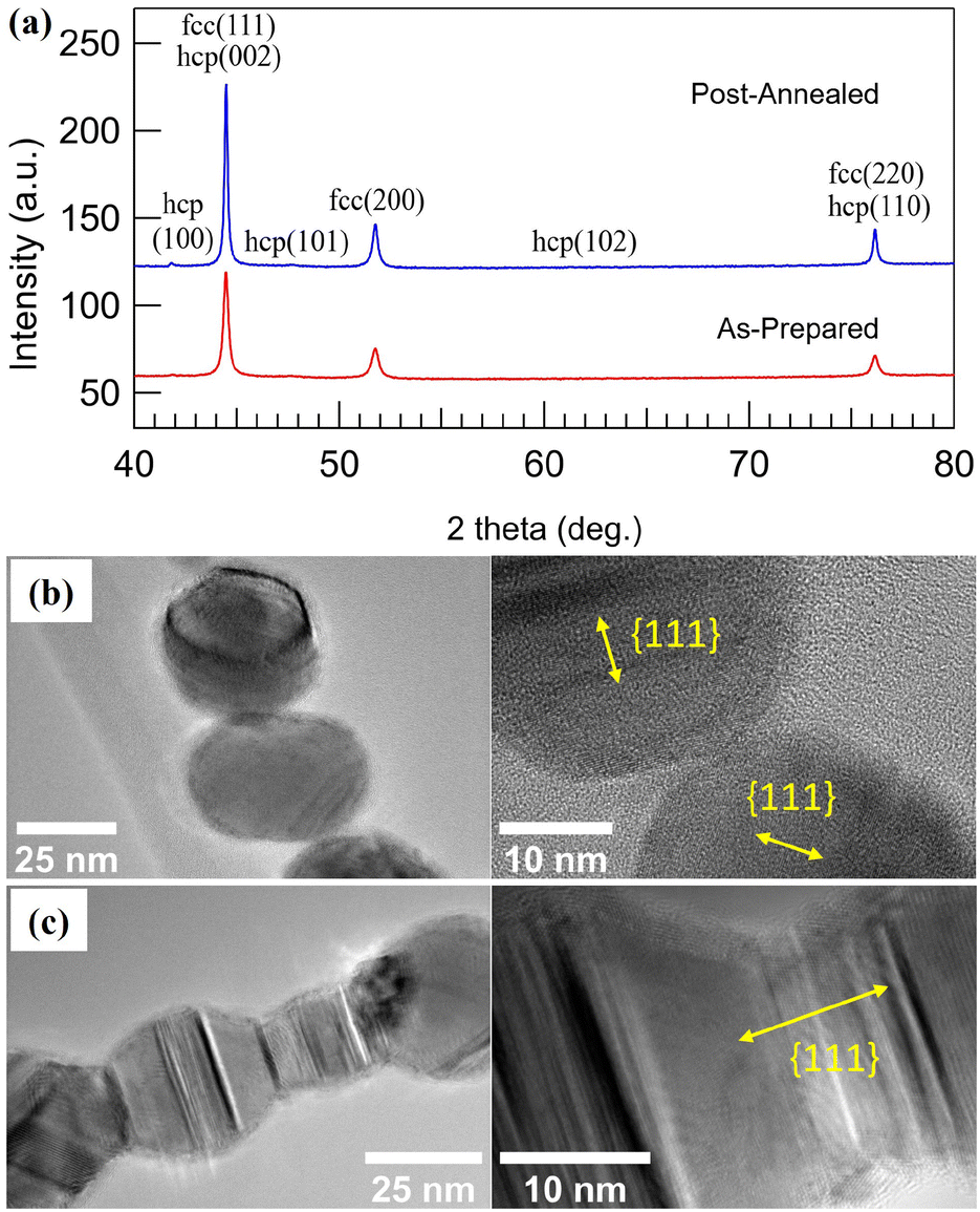 | ||
| Fig. 2 (a) XRD diffractograms of as-prepared, and post-annealed Co nanoparticles, HRTEM images of (b) NCs, and (c) NWs formed by post-anenaling at 773 K for 2 min. | ||
3.2. Magnetic properties
The generation technique offers a unique possibility of studying the effect on the magnetic properties as the NPs are arranged into linear 1D NCs and subsequently fused to form NWs. Fig. 3(a)–(c) shows three samples, from hereon referred to as S1, S2, and S3, composed of 3D networks of randomly oriented interconnected single chains and bundles (S1), parallel NCs generated via magnetic-field assisted self-assembly (S2), and NWs formed by post-annealing (S3). The particle coverage is the same for all three samples and was chosen to obtain a high density of 1D structures to maximize the signal for the magnetometry measurements while avoiding significant bundle formation. The NCs and NWs have large variations in lengths and co-exist with much smaller structures such as dimers, trimers, and single NPs. However, as will be demonstrated, the magnetization reversal becomes independent of length for relatively short NCs and NWs. Consequently, differences between the samples can be directly correlated with aligning the NPs into parallel NCs and forming NWs by post-annealing. Fig. 3(d)–(f) displays magnetization curves recorded from the three samples while applying a magnetic field along one of two orthogonal in-plane directions. Whereas the total magnetic moment at 1.8 T (m1.8 T) is almost identical for the three samples (Table 1), the remanence and coercivity are significantly different.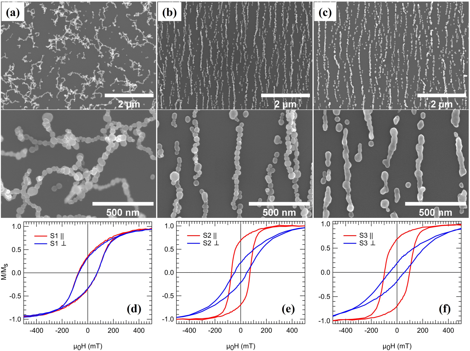 | ||
| Fig. 3 SEM images of (a) randomly oriented interconnected chains, S1, (b) ordered NCs, S2, and (c) continuous NWs, S3, on quartz substrates. Magnetic hysteresis loops of (d) S1, (e) S2, and (f) S3 measured with an in-plane magnetic field oriented parallel (∥) and perpendicular (⊥) to the longitudinal direction of the NCs and NWs. | ||
| Sample | μ 0 H c∥ (mT) | μ 0 H c⊥ (mT) | M r/Ms∥ | M r/Ms⊥ | m 1.8T (nA m2) | H c∥ (2 K) (mT) |
|---|---|---|---|---|---|---|
| S1 | 73.6 | 71.9 | 0.35 | 0.33 | 135 | 155.2 |
| S2 | 72.2 | 47.2 | 0.69 | 0.22 | 125 | 170.5 |
| S3 | 97.3 | 58.0 | 0.69 | 0.19 | 137 | 279.0 |
For S1, the NPs arrange in randomly oriented 3D interconnected chains and bundles. The average particle size is below the single-domain critical diameter for Co-fcc (Dc ≈ 80 nm), and the NPs can be spontaneously magnetized in the carrier gas as they are cooled down to room temperature. Consequently, they will be attracted to the already deposited NPs via magnetic dipole–dipole interactions when reaching the substrate. Since the particle magnetization has no preferential direction, the NPs self-assemble into 3D irregular structures56 as opposed to the ordered 1D NCs obtained when applying a magnetic field (S2). The random distribution of chain-like structures leads to an isotropic magnetic response, as demonstrated by the identical shapes of hysteresis loops recorded along two orthogonal in-plane directions, see Fig. 3(d). The high aspect ratio of the NCs in S1 leads to significant shape anisotropy with a magnetic easy-axis parallel to the long axis of the chains. In contrast, the cubic magnetocrystalline anisotropy of the individual Co-fcc NPs results in easy axes along the 〈111〉 directions, which according to HRTEM data in Fig. 2(b), can be randomly oriented along the chains. Consequently, applying an external field to the randomly oriented NCs and bundles in S1 leads to competition between the magnetocrystalline and shape anisotropy. The sample magnetization saturates for sufficiently large external fields as the individual particle moments align along the applied field direction. However, the shape anisotropy dominates at low external fields and rearranges the magnetization along the randomly oriented chains. The net remanent magnetization is thus significantly reduced with a value of Mr/Ms ≈ 0.34 at 300 K. The observed value is lower than that of Mr/Ms = 0.50 expected for an isotropic distribution of the magnetic easy axes defined here by the longitudinal direction of the chains, indicating that additional effects influence the remanent magnetization, such as local fields from the randomly oriented neighboring structures.
In contrast, arranging the NPs into parallel NCs (S2) results in a highly anisotropic system, as evident from the significantly different coercive fields Hc and reduced magnetization Mr/Ms along and perpendicular to the chain-axis, see Fig. 3(d) and (e) and Table 1. Measuring with the applied field along the chains results in an almost 100% increase in the remanent magnetization compared to S1. The increase can be understood again by the effect of the shape anisotropy, which is colinear with the NCs and the applied magnetic field. On the other hand, fusing the NPs to form NWs results in a ≈35% increase in the coercivity compared to S2. The increase in coercivity can not only be attributed to the shape anisotropy, as it scales with aspect ratio. Fig. 4(a) and (b) shows the size distribution of structures in S2 and S3 obtained by SEM image analysis over a large representing area (see the ESI†) and plotting the relative covered area by NCs or NWs with different sizes. It is observed that in the average size of the structures, the peak position in Fig. 4(a) and (b), does not vary considerably after the post-annealing to be accounted for the changes in coercivity and thus effects other than shape anisotropy must be responsible for the increased coercivity that is investigated by micromagnetic simulations. There is, however, a small decrease in the number 1D structures with length >1200 nm in Fig. 4(b) which can be attributed to the fragmentation of NWs during the post-annealing.76,77
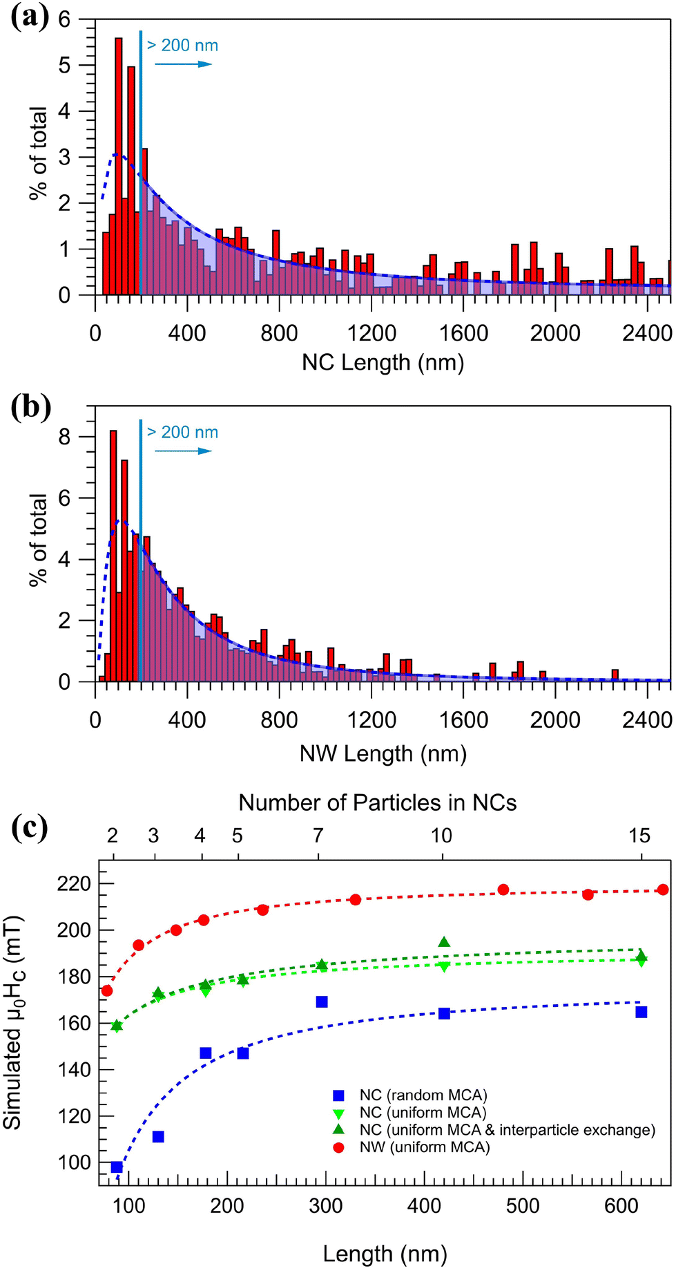 | ||
| Fig. 4 Histograms displaying the percentage of the total number of 1D structures (weighted by area) exhibiting a specific length for NCs (a) and NWs (b). The bottom axis shows calculated length assuming an average 40 nm diameter, the curves are guide to the eye. (c) Simulated coercivity values of NCs and NWs per length. | ||
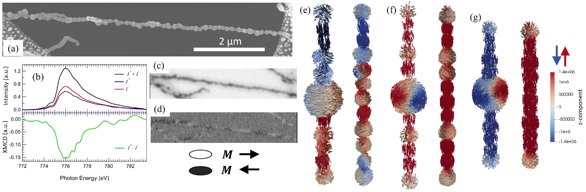 | ||
| Fig. 5 (a) SEM image of a freestanding NC, (b) nano-XAS and XMCD recorded from the NCs. (c) STXM, and (d) STXM-XMCD images of the NC. Simulated equilibrium magnetization configuration after perpendicularly magnetizing NCs with and without the inclusion of a multi-domain particle, with (e) random cubic anisotropy, and (f) uniform cubic anisotropy. (g) The simulated equilibrium state of a NC with fused particles and uniform cubic anisotropy. The red–blue color code represents the projection of the magnetization along the z-direction parallel to the chain axis. | ||
Fig. 5(a) and (c) display an SEM and an STXM image from a free-standing NC self-assembled directly along a TEM grid and post-annealed at 776 K for 2 min. While fusing has started at some of the interparticle boundaries, most NPs still maintain their original shape, and the structure can be expected to be more NC than NW-like. Before the measurement, the sample was magnetized perpendicular to the chain axis using a 7 T ex situ field. The remanent state, shown in Fig. 5(d), was imaged corresponding to the equilibrium magnetic configuration adopted by the system as it relaxes after the field have been removed. The appearance of bright and dark XMCD contrast demonstrates the presence of domains with the magnetization predominately lying along the chain axis but in different directions. Considering that the NC is far from uniform, it is likely that the emergence of magnetic domains originates from local structural variations along the chain. This is supported by the observation of domains placed at irregular distances from each other. Whereas the average particle size is below the single-domain critical diameter Dc ≈ 80 nm for Co-fcc, there are large multi-domain particles along the chain that could act as nucleation centers that initiate the domain formation as observed in diameter-modulated cylindrical NWs.79 Moreover, different directions of the MCA could be expected along the chain as the NPs have not fused to form a NW.
To gain insights into the mechanisms behind the domain formation, micromagnetic simulations were performed on NCs made up of NPs ranging from 30 to 50 nm, with and without the inclusion of a larger 100 nm multi-domain particle and also considering uniform and random MCA orientations. The magnetization configurations were obtained by minimizing the energy after saturating the NC perpendicular to the chain axis which is shown in Fig. 5(e) and (f). In addition, the equilibrium magnetization configuration for a NW, with fused particles, was simulated in the same way shown in Fig. 5(g). The simulations suggest that the randomly oriented MCA results in domain formation along the chains. Morover, when including a larger NP in the chain, the domain wall is preferably formed in the multi-domain particle in the form of a vortex. In contrast, domains are not formed in NCs or NWs when considering uniform MCA with longitudinal easy-axis (Fig. 5(f) and (g)), suggesting that the domain formation with irregular distances in Fig. 5(d) is governed by the randomness of the MCA, and local variations in the size of particles along a chain.
Furthermore, the magnetization reversal of individual NCs was studied using STXM and in situ magnetic fields applied along the chain-axis. Fig. 6(a) and (b) shows an SEM and STXM image from the same two NCs, one short composed of 4 NPs (NC1) and one much longer with a length of about 2 μm (NC2). The STXM image clearly reproduces the structural features with the larger NPs along the longer chain clearly visible. Fig. 6(c) displays the spatially resolved XMCD signal while applying an in-plane 140 mT in situ magnetic field along the positive z-direction. Note that the in situ field is parallel to the field applied during the self-assembly and thus also aligned with the remanent magnetization. As expected, the resulting magnetic contrast demonstrates a homogeneous magnetization along the NC parallel to the applied field and the remanent magnetization (bright contrast). Reversing the magnetic field results in the shorter chain (NC1) switching its magnetization (dark contrast), see Fig. 6(d). The switching can be explained by the small shape anisotropy of the shorter chain, allowing the weak in situ field of −140 mT to reverse the magnetization. Magnetization switching under the −140 mT field is also observed in a region along NC2 where switching occurs in the middle of the chain close to a significantly larger NP, indicated by arrows in Fig. 6(a) and (d).
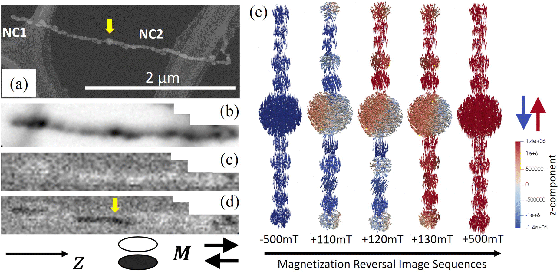 | ||
| Fig. 6 (a) SEM image of a short (NC1) and a long (NC2) chain. (b) STXM image from the same area. Magnetic contrast after magnetizing along (c) +z and (d) −z using in situ fields of ±140 mT. (e) Magnetization reversal sequences while sweeping the field from −500 to +500 mT along the chain axis. The red–blue color code represents the projection of the magnetization along the z-direction parallel to the chain axis. Note that the particle magnetization, given by the arrows, can also have x–y components during the reversal, which will be important for the magnetotransport properties of the NCs. | ||
To further study the impact of multi-domain particles during the magnetization reversal process in NCs, micromagnetic simulations were conducted on a chain with an inclusion of a 100 nm particle. Fig. 6(e) selectively illustrates the magnetization configuration of the NC as the magnetic field is swept from −500 mT to +500 mT along the chain (z-direction). The results reveal that the magnetization reversal starts from variations in the spin structure of the large particle shell and also particles located at the ends of the chain. The process continues with the formation of a vortex inside the larger particle, the emergence of transverse magnetization configurations in the NPs at 110 mT, and magnetization switching of the half of the NC at around 120 mT. By further increasing the field, the other half of the chain reverses its magnetization along the +z-direction, at +500 mT the system reaches saturation with the magnetization lying along the chain axis. The results are consistent with the STXM-XMCD measurements in Fig. 6 and emphasize the effect of multi-domain particles in the magnetization reversal.
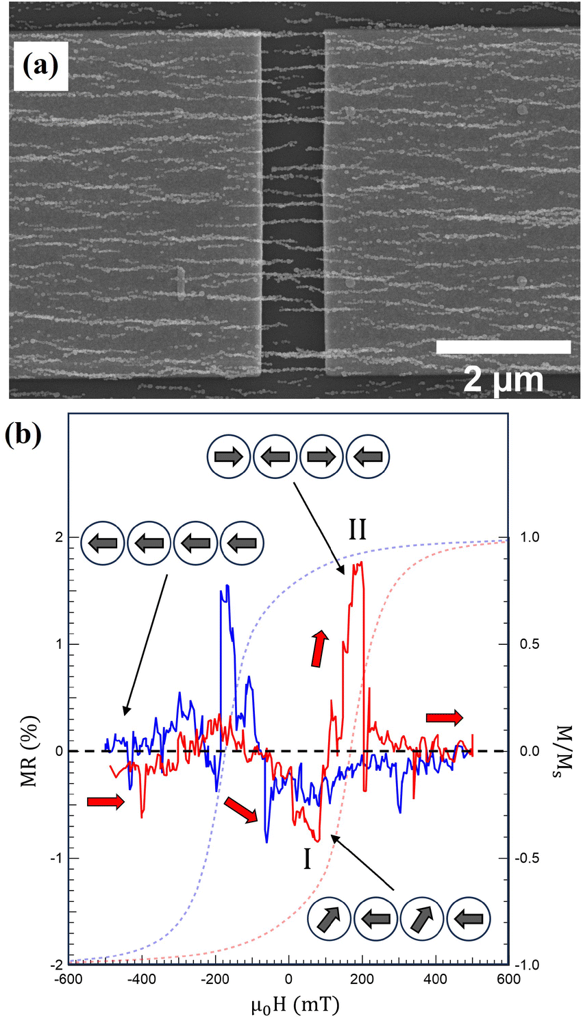 | ||
| Fig. 7 (a) SEM image of Co NCs directly self-assembled across a 1 μm gap between the source and drain. (b) MR behavior measured using a constant bias voltage of −0.5 V while varying a magnetic field along the chain axis at 25 mK. The arrows and schematic magnetization configurations correspond to sweeping the magnetic field from −500 mT in the positive direction. Similar behavior is observed when sweeping the field in the opposite direction (blue MR curve), but arrows and schematic magnetization configuration has been omitted for clarity. Also shown is a hysteresis loop recorded from S2 at 2 K. | ||
The device in Fig. 7 is one out of seven produced on the same Si chip, of which six exhibit MR behavior with changes in the resistivity around the nucleation and coercive fields, see Fig. S4.† It should be noted that the source and drain are contacted through a set of parallel unique NCs with different nanoscale structures. As demonstrated, variations in the MCA and the size of the NPs along the NCs influence the domain formation and magnetization reversal. Subsequently, the two MR contributions denoted I and II above can vary in magnitude between the devices. The main contribution for devices 1 and 4 comes from domain formation at Hc with an increase in MR, whereas a decrease due to transverse magnetization components dominates in devices 2 and 5. For device 3, both mechanisms contribute equally, and for device 6, a more complex MR behavior is observed.
4. Conclusions
This work presents the first magnetotransport study of metallic NCs integrated into devices. The magnetoresistive elements were directly integrated using a novel template-free approach with directed self-assembly of gas-phase generated NPs using a combination of electric and magnetic fields. Measuring the electric conductance reveals an MR of 0.5–1.8%, providing proof of principle for facile fabrication of magnetoresistive devices based on 1D nanogranular sensing elements. Furthermore, the study presents the first investigation into the effect on the magnetic properties as 1D nano-granular systems are transformed into single-crystalline NWs. By combining magnetometry, X-ray microscopy, and micromagnetic simulations, we demonstrate how interparticle interactions, local variations in the MCA, and the size of the individual NPs play a crucial role in domain formation and magnetization reversal.Author contributions
Mehran Sedrpooshan: Conceptualization, investigation, data curation, formal analysis, writing – original draft. Claudiu Bulbucan: Investigation, data curation, formal analysis, writing – review & editing. Pau Ternero: Investigation, data curation, writing – review & editing. Pierfrancesco Maltoni: Investigation, data curation, formal analysis, writing – review & editing. Calle Preger: Investigation, formal analysis, writing – review & editing. Simone Finizio: Data curation, writing – review & editing. Benjamin Watts: Data curation, writing – review & editing. Davide Peddis: Writing – review & editing, supervision, funding acquisition. Adam M. Burke: Investigation, formal analysis, writing – review & editing, supervision. Maria E. Messing: Conceptualization, writing – review & editing, supervision, funding acquisition. Rasmus Westerström: Conceptualization, formal analysis, writing – original draft, supervision, funding acquisition.Conflicts of interest
The authors declare no potential conflict of interest.Acknowledgements
This research received funding from the European Union's H2020 MSCA (Grant No. 945378) (GenerationNano), the Swedish Research Council (Grant No. 2019-04970), the Swedish Energy Agency (Grant No. 50689-1), the Crafoord Foundation, and NanoLund. Part of the experimental work was performed in Lund Nano Lab, part of Myfab research infrastructure. We acknowledge MAX IV Laboratory for time on Beamline SoftiMAX under Proposal 20200688. Research conducted at MAX IV, a Swedish national user facility, is supported by the Swedish Research Council under contract 2018-07152, the Swedish Governmental Agency for Innovation Systems under contract 2018-04969, and Formas under contract 2019-02496. Part of this work was performed at the PolLux (X07DA) beamline of the Swiss Light Source, Paul Scherrer Institut, Villigen PSI, Switzerland. The PolLux endstation was financed by the German Bundesministerium für Bildung und Forschung (BMBF) under contract numbers 05K16WED and 05K19WE2. We acknowledge Thomas Greber for providing access to the SQUID under Swiss National Science Foundation Grant No. 206021_150784 (Requip ASKUZI). DP and PM thank Gaspare Varvaro (CNR-ISM, Rome) for useful discussion and Enrico Patrizi (CNR-ISM) for technical assistance in magnetization measurements.References
- R. Streubel, P. Fischer, F. Kronast, V. P. Kravchuk, D. D. Sheka, Y. Gaididei, O. G. Schmidt and D. Makarov, J. Phys. D: Appl. Phys., 2016, 49, 363001 CrossRef.
- A. Fernández-Pacheco, R. Streubel, O. Fruchart, R. Hertel, P. Fischer and R. P. Cowburn, Nat. Commun., 2017, 8, 1–14 CrossRef PubMed.
- S. S. Parkin, M. Hayashi and L. Thomas, Science, 2008, 320, 190–194 CrossRef CAS PubMed.
- S. Parkin and S.-H. Yang, Nat. Nanotechnol., 2015, 10, 195–198 CrossRef CAS PubMed.
- Y. P. Ivanov, A. Chuvilin, S. Lopatin and J. Kosel, ACS Nano, 2016, 10, 5326–5332 CrossRef CAS PubMed.
- C. Bran, E. Berganza, J. A. Fernandez-Roldan, E. M. Palmero, J. Meier, E. Calle, M. Jaafar, M. Foerster, L. Aballe and A. Fraile Rodriguez, et al. , ACS Nano, 2018, 12, 5932–5939 CrossRef CAS PubMed.
- T. da Câmara Santa Clara Gomes, N. Marchal, F. Abreu Araujo and L. Piraux, Nanomaterials, 2020, 10, 2092 CrossRef PubMed.
- Z.-M. Liao, Y.-D. Li, J. Xu, J.-M. Zhang, K. Xia and D.-P. Yu, Nano Lett., 2006, 6, 1087–1091 CrossRef CAS PubMed.
- V. E. Demidov, S. Urazhdin, H. Ulrichs, V. Tiberkevich, A. Slavin, D. Baither, G. Schmitz and S. O. Demokritov, Nat. Mater., 2012, 11, 1028–1031 CrossRef CAS PubMed.
- J. Guzmán-Mínguez, S. Ruiz-Gómez, L. Vicente-Arche, C. Granados-Miralles, C. Fernández-González, F. Mompeán, M. García-Hernández, S. Erohkin, D. Berkov and D. Mishra, et al. , ACS Appl. Nano Mater., 2020, 3, 9842–9851 CrossRef.
- J. Mohapatra, M. Xing, J. Elkins, J. Beatty and J. P. Liu, Adv. Funct. Mater., 2021, 31, 2010157 CrossRef CAS.
- S. Raviolo, F. Tejo, N. Bajales and J. Escrig, Mater. Res. Express, 2018, 5, 015043 CrossRef.
- C. Bran, J. A. Fernandez-Roldan, R. P. Del Real, A. Asenjo, Y.-S. Chen, J. Zhang, X. Zhang, A. Fraile Rodríguez, M. Foerster and L. Aballe, et al. , ACS Nano, 2020, 14, 12819–12827 CrossRef CAS PubMed.
- M. Staňo and O. Fruchart, Handbook of magnetic materials, Elsevier, 2018, vol. 27, pp. 155–267 Search PubMed.
- J. M. De Teresa, Nanofabrication: Nanolithography techniques and their applications, IOP Publishing, 2020 Search PubMed.
- A. Fernández-Pacheco, L. Skoric, J. M. De Teresa, J. Pablo-Navarro, M. Huth and O. V. Dobrovolskiy, Materials, 2020, 13, 3774 CrossRef PubMed.
- A. Fernández-Pacheco, L. Serrano-Ramón, J. M. Michalik, M. R. Ibarra, J. M. De Teresa, L. O'Brien, D. Petit, J. Lee and R. P. Cowburn, Sci. Rep., 2013, 3, 1–5 Search PubMed.
- J. Pablo-Navarro, C. Magén and J. M. De Teresa, ACS Appl. Nano Mater., 2017, 1, 38–46 CrossRef.
- C. Magén, J. Pablo-Navarro and J. M. De Teresa, Nanomaterials, 2021, 11, 402 CrossRef PubMed.
- D. Liu, S. Li, T. Zhang, H. Jiang and Y. Lu, ACS Appl. Mater. Interfaces, 2021, 13, 36157–36170 CrossRef CAS PubMed.
- E. Alphandery, S. Faure, O. Seksek, F. Guyot and I. Chebbi, ACS Nano, 2011, 5, 6279–6296 CrossRef CAS PubMed.
- S. A. Corr, S. J. Byrne, R. Tekoriute, C. J. Meledandri, D. F. Brougham, M. Lynch, C. Kerskens, L. O'Dwyer and Y. K. Gun'ko, J. Am. Chem. Soc., 2008, 130, 4214–4215 CrossRef CAS PubMed.
- W. You, K. Pei, L. Yang, X. Li, X. Shi, X. Yu, H. Guo and R. Che, Nano Res., 2020, 13, 72–78 CrossRef CAS.
- J. Liu, M.-S. Cao, Q. Luo, H.-L. Shi, W.-Z. Wang and J. Yuan, ACS Appl. Mater. Interfaces, 2016, 8, 22615–22622 CrossRef CAS PubMed.
- S. Ekeroth, J. Ekspong, D. K. Perivoliotis, S. Sharma, R. Boyd, N. Brenning, E. Gracia-Espino, L. Edman, U. Helmersson and T. Wågberg, ACS Appl. Nano Mater., 2021, 4, 12957–12965 CrossRef CAS.
- S. Ekeroth, E. P. Münger, R. Boyd, J. Ekspong, T. Wågberg, L. Edman, N. Brenning and U. Helmersson, Nano Lett., 2018, 18, 3132–3137 CrossRef CAS PubMed.
- B. Su, Y. Wu, Y. Tang, Y. Chen, W. Cheng and L. Jiang, Adv. Mater., 2013, 25, 3968–3972 CrossRef CAS PubMed.
- M. Xiong, X. Jin and J. Ye, Nanoscale, 2016, 8, 4991–4999 RSC.
- R. J. Tseng, C. Tsai, L. Ma, J. Ouyang, C. S. Ozkan and Y. Yang, Nat. Nanotechnol., 2006, 1, 72–77 CrossRef CAS PubMed.
- X. Jiang, J. Feng, L. Huang, Y. Wu, B. Su, W. Yang, L. Mai and L. Jiang, Adv. Mater., 2016, 28, 6952–6958 CrossRef CAS PubMed.
- Y. Tang, B. Su, M. Liu, Y. Feng, X. Jiang, L. Jiang and A. Yu, Small, 2017, 13, 1601087 CrossRef PubMed.
- S. Singamaneni, V. N. Bliznyuk, C. Binek and E. Y. Tsymbal, J. Mater. Chem., 2011, 21, 16819–16845 RSC.
- B. H. Zhou and J. D. Rinehart, ACS Cent. Sci., 2018, 4, 1222–1227 CrossRef CAS PubMed.
- F. Fabris, E. Lima Jr., C. Quinteros, L. Nener, M. Granada, M. Sirena, R. D. Zysler, H. E. Troiani, V. Leborán and F. Rivadulla, et al. , Phys. Rev. Appl., 2019, 11, 054089 CrossRef CAS.
- C. Jiang, S. M. Ng, C. W. Leung and P. W. Pong, J. Mater. Chem. C, 2017, 5, 252–263 RSC.
- C. Jiang, P. H. Chan, C. W. Leung and P. W. Pong, J. Phys. Chem. C, 2017, 121, 22508–22516 CrossRef CAS.
- C. Black, C. Murray, R. Sandstrom and S. Sun, Science, 2000, 290, 1131–1134 CrossRef CAS PubMed.
- M. Pauly, J.-F. Dayen, D. Golubev, J.-B. Beaufrand, B. P. Pichon, B. Doudin and S. Bégin-Colin, Small, 2012, 8, 108–115 CrossRef CAS PubMed.
- C. Jiang, C. W. Leung and P. W. Pong, Appl. Surf. Sci., 2017, 419, 692–696 CrossRef CAS.
- L. Chen, B. Su and L. Jiang, Chem. Soc. Rev., 2019, 48, 8–21 RSC.
- A. McMullen, M. Holmes-Cerfon, F. Sciortino, A. Y. Grosberg and J. Brujic, Phys. Rev. Lett., 2018, 121, 138002 CrossRef CAS PubMed.
- D. Toulemon, M. V. Rastei, D. Schmool, J. S. Garitaonandia, L. Lezama, X. Cattoën, S. Bégin-Colin and B. P. Pichon, Adv. Funct. Mater., 2016, 26, 2454–2462 CrossRef CAS.
- J. Wang, Q. Chen, C. Zeng and B. Hou, Adv. Mater., 2004, 16, 137–140 CrossRef CAS.
- W. Zhang, P. K. J. Wong, D. Zhang, J. Yue, Z. Kou, G. van der Laan, A. Scholl, J.-G. Zheng, Z. Lu and Y. Zhai, Adv. Funct. Mater., 2017, 27, 1701265 CrossRef.
- Z. Kou, E. Liu, J. Yue, Y. Sui, Z. Huang, D. Zhang, Y. Wang, Y. Zhai, J. Du and H. Zhai, J. Appl. Phys., 2015, 117, 17E709 CrossRef.
- Y. Zhang, L. Sun, Y. Fu, Z. Huang, X. Bai, Y. Zhai, J. Du and H. Zhai, J. Phys. Chem. C, 2009, 113, 8152–8157 CrossRef CAS.
- G. Cheng, D. Romero, G. T. Fraser and A. Hight Walker, Langmuir, 2005, 21, 12055–12059 CrossRef CAS PubMed.
- Y. Chen and A. El-Ghazaly, Small, 2022, 2205079 Search PubMed.
- P. Liu, Z. Li, B. Zhao, B. Yadian and Y. Zhang, Mater. Lett., 2009, 63, 1650–1652 CrossRef CAS.
- G. Lee, S. Huh, J. Park, H.-C. Ri and J. Jeong, J. Phys. Chem. B, 2002, 106, 2123–2126 CrossRef CAS.
- E. Athanassiou, P. Grossmann, R. Grass and W. J. Stark, Nanotechnology, 2007, 18, 165606 CrossRef.
- T. Kraus, L. Malaquin, H. Schmid, W. Riess, N. D. Spencer and H. Wolf, Nat. Nanotechnol., 2007, 2, 570–576 CrossRef CAS PubMed.
- B. Su, C. Zhang, S. Chen, X. Zhang, L. Chen, Y. Wu, Y. Nie, X. Kan, Y. Song and L. Jiang, Adv. Mater., 2014, 26, 2501–2507 CrossRef CAS PubMed.
- W. Jung, Y.-H. Jung, P. V. Pikhitsa, J. Feng, Y. Yang, M. Kim, H.-Y. Tsai, T. Tanaka, J. Shin and K.-Y. Kim, et al. , Nature, 2021, 592, 54–59 CrossRef CAS PubMed.
- B. Liu, S. Liu, V. Devaraj, Y. Yin, Y. Zhang, J. Ai, Y. Han and J. Feng, Nat. Commun., 2023, 14, 4920 CrossRef CAS PubMed.
- C. Preger, M. Josefsson, R. Westerström and M. E. Messing, Nanotechnology, 2021, 32, 195603 CrossRef CAS PubMed.
- G. Biskos, V. Vons, C. U. Yurteri and A. Schmidt-Ott, KONA Powder Part. J., 2008, 26, 13–35 CrossRef.
- P. Ternero, M. Sedrpooshan, D. Wahlqvist, B. O. Meuller, M. Ek, J.-M. Hübner, R. Westerström and M. E. Messing, J. Aerosol Sci., 2023, 170, 106146 CrossRef CAS.
- C. Preger, C. Bulbucan, B. O. Meuller, L. Ludvigsson, A. Kostanyan, M. Muntwiler, K. Deppert, R. Westerström and M. E. Messing, J. Phys. Chem. C, 2019, 123, 16083–16090 CrossRef CAS.
- C. Bulbucan, C. Preger, A. Kostanyan, K. M. Jensen, E. Kokkonen, C. Piamonteze, M. E. Messing and R. Westerström, Nanoscale, 2021, 13, 15844–15852 RSC.
- C. Bulbucan, P. Ternero, C. Preger, A. Kostanyan, M. E. Messing and R. Westerström, J. Magn. Magn. Mater., 2023, 170359 CrossRef CAS.
- B. H. Zhou and J. D. Rinehart, ACS Appl. Electron. Mater., 2019, 1, 1065–1069 CrossRef CAS.
- H. Lehmann, S. Willing, S. Möller, M. Volkmann and C. Klinke, Nanoscale, 2016, 8, 14384–14392 RSC.
- K. Yakushiji, S. Mitani, F. Ernult, K. Takanashi and H. Fujimori, Phys. Rep., 2007, 451, 1–35 CrossRef CAS.
- A. Schmidt-Ott, Spark Ablation: Building Blocks for Nanotechnology, CRC Press, 2019 Search PubMed.
- C. Preger, N. C. Overgaard, M. E. Messing and M. H. Magnusson, Aerosol Sci. Technol., 2020, 54, 718–728 CrossRef CAS.
- J. Dixkens and H. Fissan, Aerosol Sci. Technol., 1999, 30, 438–453 CrossRef CAS.
- J. Raabe, G. Tzvetkov, U. Flechsig, M. Böge, A. Jaggi, B. Sarafimov, M. Vernooij, T. Huthwelker, H. Ade and D. Kilcoyne, et al. , Rev. Sci. Instrum., 2008, 79, 113704 CrossRef CAS PubMed.
- J. Schwenke, K. Thanell, I. Beinik, L. Roslund and T. Tyliszczak, Microsc. Microanal., 2018, 24, 232–233 CrossRef.
- K. Thanell, W. Grizolli, K. Klementiev and R. Sankari, Microsc. Microanal., 2018, 24, 326–327 CrossRef.
- M. Beg, M. Lang and H. Fangohr, IEEE Trans. Magn., 2022, 58, 1–5 Search PubMed.
- M. J. Donahue and M. Donahue, OOMMF user's guide, version 1.0, US Department of Commerce, National Institute of Standards and Technology, 1999 Search PubMed.
- R. N. Grass and W. J. Stark, J. Mater. Chem., 2006, 16, 1825–1830 RSC.
- J. Feng, L. Huang, L. Ludvigsson, M. E. Messing, A. Maisser, G. Biskos and A. Schmidt-Ott, J. Phys. Chem. C, 2016, 120, 621–630 CrossRef CAS.
- H. Sato, O. Kitakami, T. Sakurai, Y. Shimada, Y. Otani and K. Fukamichi, J. Appl. Phys., 1997, 81, 1858–1862 CrossRef CAS.
- T. Hawa and M. Zachariah, Phys. Rev. B: Condens. Matter Mater. Phys., 2007, 76, 054109 CrossRef.
- M. Toimil Molares, A. Balogh, T. Cornelius, R. Neumann and C. Trautmann, Appl. Phys. Lett., 2004, 85, 5337–5339 CrossRef CAS.
- L. Vivas, R. Yanes, O. Chubykalo-Fesenko and M. Vazquez, Appl. Phys. Lett., 2011, 98, 232507 CrossRef.
- S. Allende, D. Altbir and K. Nielsch, Phys. Rev. B: Condens. Matter Mater. Phys., 2009, 80, 174402 CrossRef.
- B. Hausmanns, T. P. Krome, G. Dumpich, E. F. Wassermann, D. Hinzke, U. Nowak and K.-D. Usadel, J. Magn. Magn. Mater., 2002, 240, 297–300 CrossRef CAS.
- U. Ebels, A. Radulescu, Y. Henry, L. Piraux and K. Ounadjela, Phys. Rev. Lett., 2000, 84, 983 CrossRef CAS PubMed.
Footnote |
| † Electronic supplementary information (ESI) available. See DOI: https://doi.org/10.1039/d3nr03878e |
| This journal is © The Royal Society of Chemistry 2023 |