
 Open Access Article
 This Open Access Article is licensed under a
 Creative Commons Attribution 3.0 Unported Licence
Optical properties of orthorhombic germanium sulfide: unveiling the anisotropic nature of Wannier excitons†
Mehdi
Arfaoui
 *a,
Natalia
Zawadzka
b,
Sabrine
Ayari
c,
Zhaolong
Chen
de,
Kenji
Watanabe
f,
Takashi
Taniguchi
g,
Adam
Babiński
b,
Maciej
Koperski
de,
Sihem
Jaziri
a and
Maciej R.
Molas
b
*a,
Natalia
Zawadzka
b,
Sabrine
Ayari
c,
Zhaolong
Chen
de,
Kenji
Watanabe
f,
Takashi
Taniguchi
g,
Adam
Babiński
b,
Maciej
Koperski
de,
Sihem
Jaziri
a and
Maciej R.
Molas
b
aLaboratoire de Physique de la Matière Condensée, Département de Physique, Faculté des Sciences de Tunis, Université Tunis El Manar, Campus Universitaire, 1060 Tunis, Tunisia. E-mail: mehdi.arfaoui@fst.utm.tn
bInstitute of Experimental Physics, Faculty of Physics, University of Warsaw, Warsaw, Poland. E-mail: maciej.molas@fuw.edu.pl
cLaboratoire de Physique de l'Ecole normale supérieure, ENS, Université PSL, CNRS, Sorbonne Université, Université de Paris, 24 rue Lhomond, 75005 Paris, France
dInstitute for Functional Intelligent Material, National University of Singapore, 117575, Singapore
eDepartment of Materials Science and Engineering, National University of Singapore, 117575, Singapore
fResearch Center for Electronic and Optical Materials, National Institute for Materials Science, 1-1 Namiki, Tsukuba 305-0044, Japan
gResearch Center for Materials Nanoarchitectonics, National Institute for Materials Science, 1-1 Namiki, Tsukuba 305-0044, Japan
First published on 16th October 2023
Abstract
To fully explore exciton-based applications and improve their performance, it is essential to understand the exciton behavior in anisotropic materials. Here, we investigate the optical properties of anisotropic excitons in GeS encapsulated by h-BN using different approaches that combine polarization- and temperature-dependent photoluminescence (PL) measurements, ab initio calculations, and effective mass approximation (EMA). Using the Bethe–Salpeter Equation (BSE) method, we found that the optical absorption spectra in GeS are significantly affected by the Coulomb interaction included in the BSE method, which shows the importance of excitonic effects besides it exhibits a significant dependence on the direction of polarization, revealing the anisotropic nature of bulk GeS. By combining ab initio calculations and EMA methods, we investigated the quasi-hydrogenic exciton states and oscillator strength (OS) of GeS along the zigzag and armchair axes. We found that the anisotropy induces lifting of the degeneracy and mixing of the excitonic states in GeS, which results in highly non-hydrogenic features. A very good agreement with the experiment is observed.
1. Introduction
The groundbreaking discovery of graphene and its unique properties has sparked further research on the development of other alternative layered and non-layered materials with various optical, electronic, and chemical properties.1,2 Recently, transition metal dichalcogenides (TMDs)3,4 and black phosphorus (BP)5,6 have been extensively researched for their high carrier mobility7–9 and strong bound excitons.6,10–12 However, the instability of BP under air conditions limits its practical use.13–15 An alternative class of materials with a puckered honeycomb lattice, group-IV monochalcogenides MX (where M = Ge, Sn, or Pb and X = S, Se, or Te),16–19 has emerged as a promising new class of layered van der Waals (vdW) semiconductors due to their benefits such as low toxicity,20 high thermal stability,21,22 Earth abundance,19,23 and excellent absorption energies observed in the visible frequency range,24–27 in addition to low thermal conductivities and significant anisotropic physical properties.19,24,28–31 Among group-IV monochalcogenides, germanium sulfide (GeS) is considered a promising material in optoelectronics applications due to its high optical absorption and optical band gap (BG) in the visible range, which can be effectively tuned by applying an external strain. This allows for modulation of its emission wavelength.32–36 GeS also exhibits high photosensitivity, a broad spectral response, and giant piezoelectricity because of its characteristic “puckered” symmetry.25,27,37 Analogously to BP, the low symmetry orthorhombic crystal structure of GeS results in unique anisotropic optical, electronic, and vibrational properties along the zigzag (ZZ) and armchair (AC) axes,35,38–41 which makes it suitable for large-scale applications in photovoltaic thermoelectric42 and optoelectronics.19 Polarization-resolved photoluminescence (PL), reflectance contrast (RC), and Raman scattering (RS) measurements performed over a wide temperature range in GeS confirmed its anisotropies characteristics.24,29,43 This makes it a highly promising material for the development of polarization-sensitive photodetectors. It is important to examine the many-body interactions present in this material, particularly with regard to the excitonic effect.27,35,40,41,44,45 Despite the tremendous progress in the study of GeS, many of its fundamental optical anisotropic properties remain unknown.24 Indeed, our study delves into the optical properties of the anisotropic nature of the Wannier excitons of GeS that remain neglected or incompletely understood in previous studies,24,29,43 using different theoretical approaches and supported by experimental results.In this work, we investigate the optical response of anisotropic excitons in GeS encapsulated with hexagonal BN (h-BN) flakes using a comprehensive approach that combines polarization- and temperature-dependent PL techniques, ab initio calculations, and effective mass approximation (EMA). The innovative point of our work originates from both the applied experimental and theoretical approaches. A high quality of the investigated sample was achieved by its preparation under an inert protective gas atmosphere, and GeS was embedded in between h-BN flakes to avoid degradation processes. Additionally, to describe the experimental results, we employed a state-of-the-art approach that utilized density functional theory (DFT) and the quasiparticle (QP) correction GW to determine the electronic band structure (BS) of bulk GeS, and the anisotropic effective mass of electrons and holes in different crystal directions. Furthermore, using both the independent particle approximation (IPA) and the GW + Bethe–Salpeter equation (BSE),46,47 we studied the dielectric functions for light polarized along the in-plane (x–y) and out-of-plane (z) directions. Indeed, the obtained result from the BSE modifies the optical absorption spectra in bulk GeS. Thus, it shows the signature of excitonic effects on the optical response. To evaluate the different optical selection rules, we calculated the direct interband optical transition matrix elements (OME) in different crystal directions, as well as the percentage of the atomic orbital contribution to the valence and conduction bands at specific k-points of the Brillouin zone (BZ). We were also able to predict the quasi-hydrogenic exciton states and the oscillator strength (OS) of the excitons along both the ZZ and AC directions by integrating ab initio calculations with the EMA. In fact, the anisotropic effect on the exciton characteristics in GeS (e.g., exciton binding energy (BE) and the spatial extension of exciton wavefunction) is controlled by its reduced mass and dielectric constant. Unlike the isotropic hydrogenic model, the anisotropy lifts the degeneracy of the exciton states, which have the same principal quantum number but different radial and angular quantum numbers. This increases in the number of allowed dipole transitions that can be probed by terahertz radiation, providing new ways of controlling device emissions.
This article is organized as follows: in section 2, we present the experimental results obtained for a GeS flake encapsulated with h-BN, which include its measured polarization- and temperature-dependent PL spectra. In section 3, to gain a deeper understanding of the exciton behavior in anisotropic materials, we used theoretical methods (DFT and GW + BSE) to calculate the electronic BS of GeS, taking into account the excitonic effect. In section 4, we analyze the anisotropic behavior of GeS using the EMA. By varying the relevant parameters, we control the degree of anisotropy across multiple cases, ranging from isotropic to anisotropic. Our calculations of the excitonic BE and OS were performed for each case. Overall, our study of GeS as a prototype system for anisotropic layered materials provides an understanding of the optical response of anisotropic excitons and can be tailored for other three-dimensional (3D) anisotropic materials.
2. Experimental results
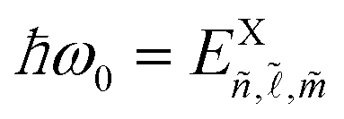
To prevent degradation of the GeS flake, we encapsulated the thick GeS flake with a thickness of about 50 nm in h-BN flakes, see Methods for details. The side-view scheme and optical image of the investigated GeS are presented in Fig. 1(a) and (b). First, we examined the polarization evolution of the PL spectra measured on the studied sample under 1.88 eV excitation, see Fig. 1(c). It is observed that the GeS emission is linearly polarized along the AC direction, whereas the PL signal is absent in the ZZ direction. Note that the attribution of the AC and ZZ directions was performed by comparison with previous results published in ref. 24, 29 and 43, and also confirmed by our theoretical calculations shown below. It is a hallmark of the anisotropic optical response of GeS. The upper panel of Fig. 1(c) presents the low-temperature (T = 5 K) PL spectra of GeS measured in two polarizations corresponding to the AC and ZZ orientations. The PL spectrum consists of three emission lines, denoted X, L1, and L2. In contrast, the corresponding polarization-resolved RC spectra, shown in section A of the ESI,† consist of a single resonance, whose energy coincides with the X emission line and is also polarized along the AC direction. We can certainly attribute the X line to the free neutral exciton,24 while the assignment of the L1 and L2 peaks is more questionable, and hence we denoted them as localized excitons, see sections A and B of the ESI† for more details. The measured shape of the PL spectrum with a rather low intensity of L1 and L2 compared to that of X is different from those reported in ref. 24. It may suggest that the hBN encapsulation plays a similar role as for MoS2 MLs, leading to complete quenching of the defect-related emission measured at liquid helium temperature.48 Interestingly, the relative intensity of the localized and free excitons strongly depends on the excitation energy, see section A of the ESI† for details. Fig. 1(d) presents the temperature evolution of the PL spectra measured from 5 K to 190 K. Our measurements indicate that with increasing temperature, the PL intensity of the exciton decreases until it completely vanishes at 200 K. This result suggests that the BE of the exciton, associated with its activation energy, is on the order of several meV. As the L1 and L2 intensities are extremely small, we used a different excitation energy, i.e., 2.41 eV, to investigate their temperature dependence (see section A in the ESI† for details). We found that at a temperature of approximately 70 K, the measured PL spectrum is contributed only by the neutral exciton line. To investigate in detail the temperature evolution of the X line, we deconvoluted it using Gaussian. The X energy shows a redshift as the temperature increases from 5 K to 190 K, see Fig. 1(e). This type of evolution, characteristic of many semiconductors, can be expressed by the relationship proposed by O'Donnell et al.,49 which describes the temperature dependence of the BG in terms of an average phonon energy 〈ℏω〉 and reads as:| Ebg(T) = Eg − S〈ℏω〉[coth(〈ℏω〉)/2kBT], | (1) |
 | (2) |
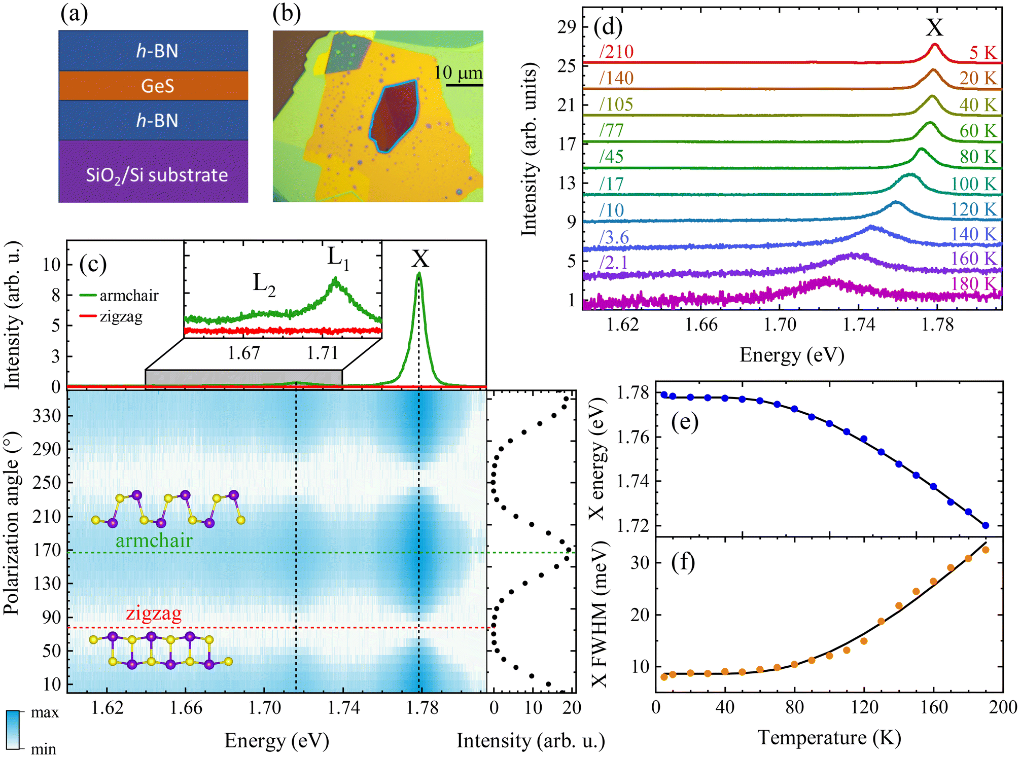 | ||
| Fig. 1 (a) Side-view scheme and (b) optical image of the investigated GeS encapsulated with h-BN flakes. (c) False-colour map of the low temperature (T = 5 K) polarization-resolved PL spectra measured on GeS flakes under excitation at 1.88 eV. Note that the intensity scale is logarithmic. The crystal structures along the ZZ and AC directions are drawn on top of the map. The top panel shows the corresponding PL spectra detected in the AC and ZZ directions. The right panel demonstrates the integrated PL intensity as a function of detection angle. (d) The corresponding temperature-dependent PL spectra measured on GeS flakes with 1.88 eV laser light excitation. The spectra are vertically shifted and are divided by scaling factors for clarity. The determined (e) energy and (f) full width at half maximum (FWHM) of the neutral exciton (X) line. The circles represent the experimental results while the curves are fits to the data obtained using eqn (1) and (2). | ||
The main objective of the present work is to construct a theoretical framework to analyze the aforementioned optical characteristics of free neutral excitons in GeS. The free exciton is identified by its distinct spectral peak located at around 1.78 eV in the PL spectra of the GeS flake with a thickness of 60 nm at T = 5 K. The low-temperature conditions stabilize and clearly define the excitonic states, yielding an accurate assessment of their spectral properties. The reduced thermal excitation also enhances the analysis of GeS's intrinsic optical properties.
3. First-principles calculations of the quasi-particle and excitonic effects in GeS
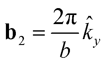
GeS is a layered material that has an orthorhombic structure and belongs to the Pnma (D2h16) space group.21 This material crystallizes in double layers. The unit cell contains eight atoms organized in two adjacent double layers. The puckered honeycomb lattice of GeS has an anisotropic crystal structure characterized by the two orthogonal AC(x) and ZZ (y) directions, as indicated in Fig. 2. The orthorhombic Bravais lattice of GeS can be specified by giving three primitive lattice vectors: a1 = a![[x with combining circumflex]](https://www.rsc.org/images/entities/i_char_0078_0302.gif) , a2 = cŷ, and a3 = cẑ, and the reciprocal primitive lattice vectors are spanned by:
, a2 = cŷ, and a3 = cẑ, and the reciprocal primitive lattice vectors are spanned by: 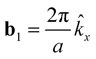 ,
,  and
and  . , ŷ and ẑ are the unit vectors in the directions of the x-axis, the y-axis, and the z-axis, respectively.
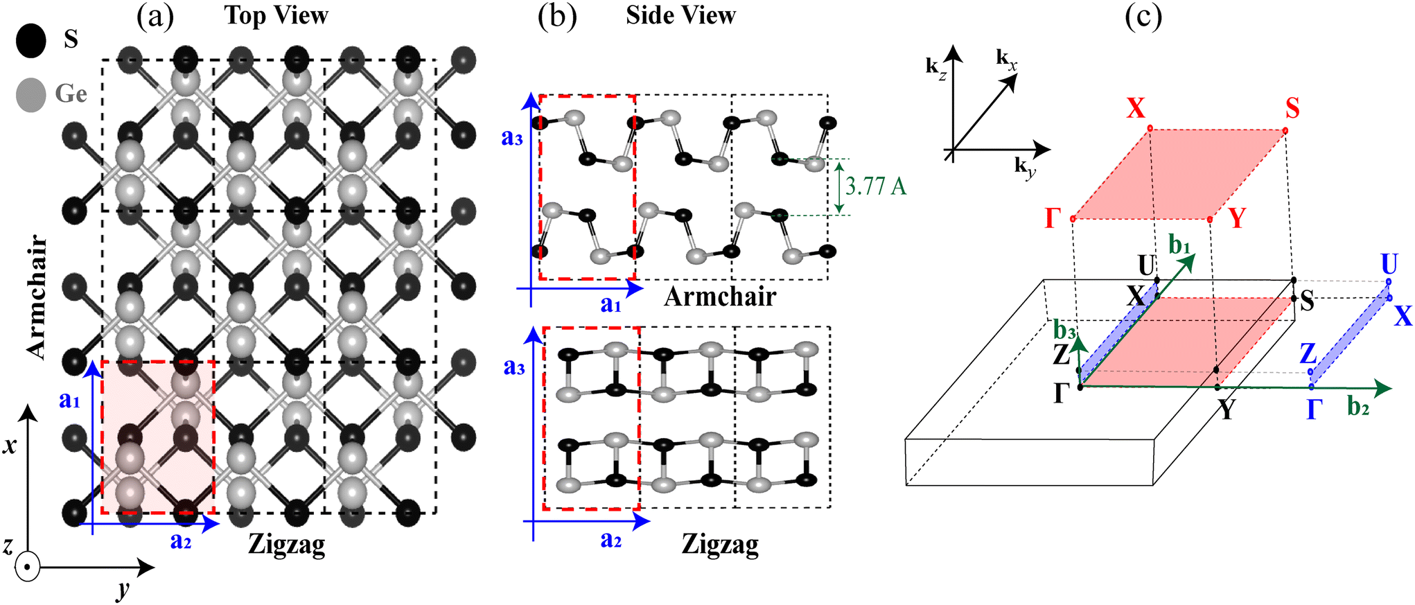 | ||
| Fig. 2 Illustration of the atomic structure of bulk GeS. (a) Top view of the atomic structure of bulk GeS in a 3 × 3 × 1 supercell. (b) Side views of bulk GeS along the AC and ZZ directions, respectively. (c) The bulk first BZ of an orthorhombic Bravais lattice and its projected surfaces. The gray and black spheres stand for the Ge and S atoms, respectively. The unit cell is indicated by the dashed red rectangle in (a and b). | ||
In Table 1, we present the final relaxed lattice parameters and compared them to previously reported experimental and theoretical data. All calculations were performed with the optimized lattice parameters.
In Fig. 3(a), we plotted the BS of bulk GeS using DFT with (black dashed curve) and without (red curve) the spin–orbit interaction. The BS of GeS is not significantly impacted by the relativistic correction effect. Therefore, we disregard this in our calculation of many-body simulations. We found that bulk GeS is a semiconductor with a BG of 1.23 eV at the Γ point. The indirect gap is only 3 meV in energy higher than the direct one. Our results are consistent with previous DFT calculations.51,52 As we can see, the DFT direct BG (red curve) has been significantly underestimated because of the BG problem with the DFT Kohn–Sham (KS) approach. To overcome this issue, we calculated the relative QP BS using the perturbative method GW (blue curve). In fact, G and W were constructed from the KS wavefunctions, and the perturbatively corrected KS eigenvalues. The single-shot G0W0 gives an insufficiently small BG when compared to the experimental one. To solve this problem, we used the self-consistency of GW on eigenvalues only (evGW), see section D in the ESI† for details. At this theoretical level, the BG increases to 1.78 eV with the QP correction of 0.55 eV at Γ. Our results are in excellent agreement with the experimental bulk GeS BG energies extrapolated to 0 K given in ref. 54 and 55, as well as with previous theoretical calculations with GW in ref. 56 and 57. In addition, the QP corrections are slightly dispersed with respect to the KS eigenenergies. In fact, we found that by fitting the QP corrections data to a linear curve, the conduction and valence bands are slightly stretched by 7% and 1%, respectively. The band profiles for the lowest conduction band and the highest valence band were also extracted from DFT and are shown in Fig. 3(b) and (c), respectively. The valence band has three maximum locations in the AC direction: K4, K3, and Γ, with the highest maximum located at the Γ-point. The conduction band has a minimum located at the Γ-point.
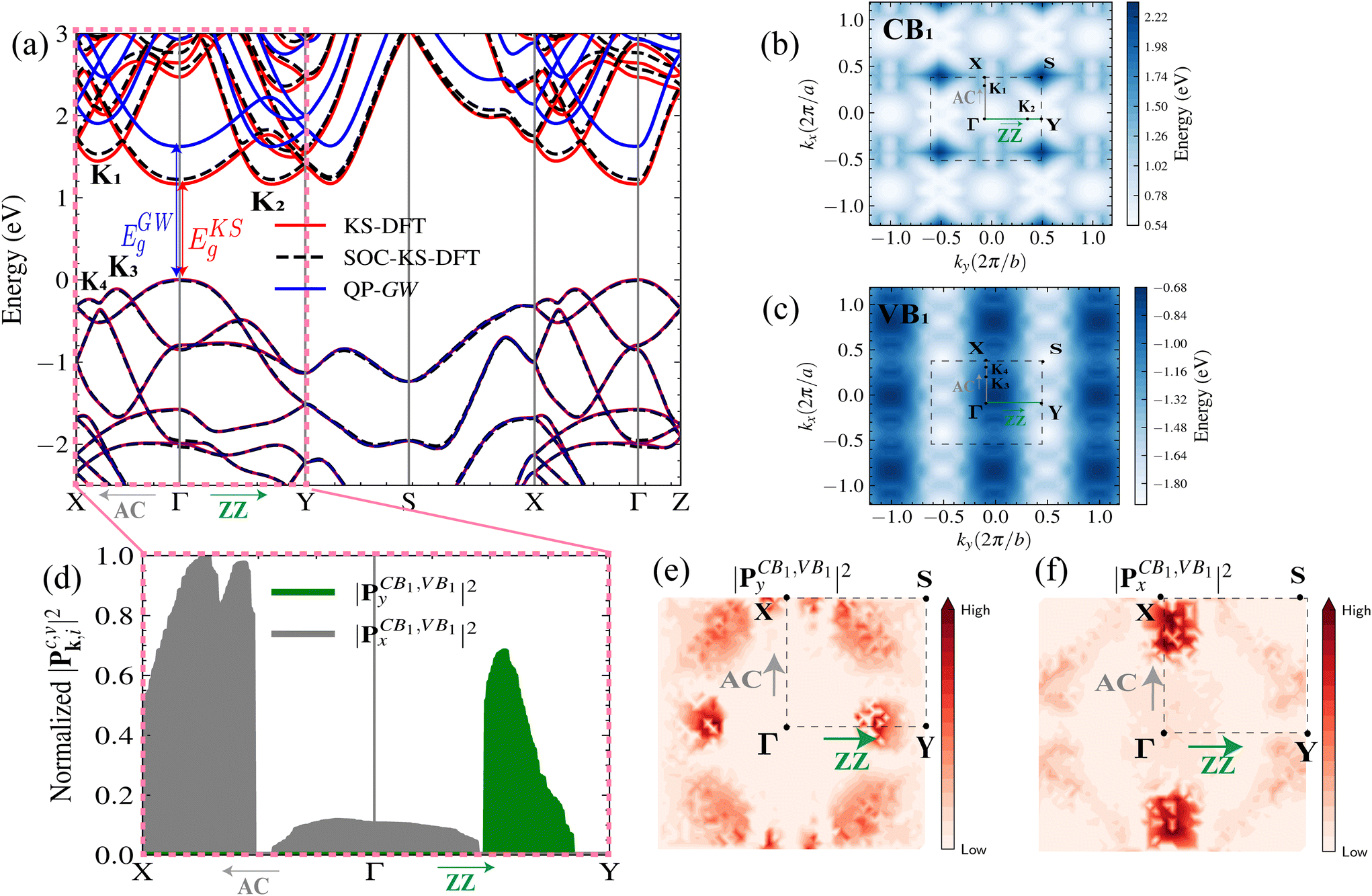 | ||
| Fig. 3 Electronic properties of GeS from ab initio calculations. (a) Electronic BS of bulk GeS calculated by generalized gradient approximation (GGA) without spin–orbit coupling (red), with spin–orbit coupling (black dashed) and evGW (blue) methods. (b) and (c) 2D BSs of the topmost valence band and the bottom most conduction band, respectively. The global maximum (minimum) of the VBM (CBM) is located at the AC direction Γ X path of the BZ. (d) Interband transitions of OME between v and c bands. (e) Color contour of the dipole OS distribution in the first BZ for light polarized in AC (e) and ZZ (f) directions derived using DFT. The darker color indicates a larger dipole strength. | ||
In Fig. 3(d–f), we calculated the normalized squared OME Mc,vi(k) = |Pc,vi|2 = |uv,k|pi|uc,k|2 between the top valence band and the bottom conduction band along a specific direction i. Here, uv(c),k is the single particle Bloch function of the valence (v) and conduction bands (c) obtained by the DFT-KS calculation for the wavevector k. pi is the momentum operator along the i direction. Mc,vi(k) measures the k-dependent optical strength of the c–v interband transition. Furthermore, the OME contain all the symmetry-imposed selection rules. Fig. 3(e) and (f) show that the k-resolved OME for light polarized in the AC and ZZ directions exhibit distinct responses, which reveals the anisotropic nature of GeS. Of particular interest are the valleys located in K1, K2, K3, K4, and Γ in the ΓX and ΓY directions, where the allowed OME are significantly higher in ΓX for light polarized in the AC direction. Additionally, the OME are not allowed in the vicinity of Γ-point for light polarized in the ZZ direction. By calculating the direct interband OME, we calculate the linear optical characteristics that can be derived from the complex dielectric tensor εi,j(ω,q) = ε1i,j(ω,q) + iε2i,j(ω,q) for q → 0, where ε1i,j(ω,q) and ε2i,j(ω,q) are the real and imaginary parts of the dielectric tensor, see sections C and D of the ESI.† ℏω is the photon energy, q is the photon wavevector and i, j = x, y, or z are the subscripts that correspond to the Cartesian directions.
In Fig. 4, we plotted the three components of the imaginary part of the dielectric function for linear light polarized along the axis of the AC (x), ZZ (y) and perpendicular (z) directions to the atomic planes for bulk GeS. In fact, Fig. 4 shows that ε2(ω) strongly depends on the direction of polarization. This behavior reveals the anisotropic character of bulk GeS. The light absorption of GeS has a wide range from near-infrared to near-ultraviolet light (1–9 eV). However, compared to the experimental results, the exciton peak does not appear in Fig. 4 with the IPA method (blue line). This result is expected since the IPA method does not include the electron–hole (e–h) interaction. To account for the e–h interaction, we plotted, in Fig. 4 (black line), the dielectric function using the GW + BSE method. A detailed description of the GW + BSE method can be found in section D of the ESI.† In fact, compared with the IPA results, the Coulomb interaction included in the BSE method modifies the optical absorption spectra in bulk GeS as well as a redistribution of OS, implying that excitonic effects have an important influence on the optical properties. The detected low-energy peak in the BSE spectrum is attributed to the presence of a bound exciton. In comparison to the experimental results, the calculated energy of the first bright exciton peak, 1.77 eV, differs by only about 10 meV from the corresponding experimental value from Fig. 1, ∼1.78 eV. In addition, our results show that GeS has remarkable optical anisotropy, as evidenced by the presence of an excitonic peak only for light polarized along the AC direction. This intriguing observation aligns very well with our experimental results in Fig. 1. The first bright exciton BE is ∼10 meV. Our experimental measurements of temperature-dependent PL spectra also support this result. In section A of the ESI,† we estimated the exciton BE to be ∼11 meV under 2.41 eV excitation, and this value can slightly increase (∼16 meV) under resonant excitation at 1.88 eV. This BE is also comparable to those of bulk materials such as BP (30 meV),58 MoS2 (25 meV),59 wurtzite GaN (21 meV)60 and GaAs quantum wells (∼10 meV).61 This is in contrast to layered group-VII TMD rhenium dichalcogenides (ReX2, where X = S, Se), which exhibit a significantly higher binding energy of 120 meV.62 Moreover, the results in the upper panel of Fig. 4 show the contributions of the occupied and unoccupied bands to ε2, where each band is labeled with a distinct index, i.e. VB1 → VB4 for the occupied bands and CB1 → CB4 for the unoccupied bands. In particular, the size of each green circle is proportional to the value of ε2(ω). Indeed, the analysis reveals that the first peak in ε2(ω) for the AC direction is predominantly formed by the direct optical transition between the occupied band VB1 and the unoccupied band CB1. Note that we neglect the phonon-assisted related optical absorption, which requires more computational resources and is beyond the scope of this work.
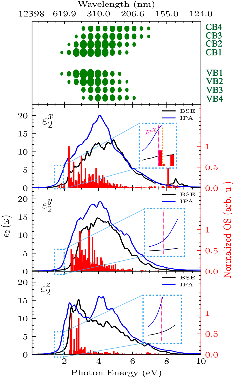 | ||
| Fig. 4 Optical properties of GeS obtained from ab initio calculations. Imaginary part of the dielectric functions calculated using IPA and GW + BSE methods, with light polarized in the x, y, and z directions, respectively. The red vertical bars represent the normalized OS (arb. units). The DFT and GW BGs are denoted by the black and orange dashed vertical lines, respectively. The size of each green circle in the upper panel corresponds to the value of ε2(ω). The theoretical value of the first bright exciton energy, EX = 1.77 eV, is marked by the dashed vertical violet line, while the dashed vertical orange line points to the corresponding experimental value of about 1.78 eV. | ||
The red shades in Fig. 5(a) show the first bright exciton weight originating from the vertical interband transition, which contributes to exciton formation and, as a result, to absorption spectra. The inset characterizes the transitions in the first reciprocal BZ. In GeS, it is mainly contributed by transitions in the nearby Γ valley along ΓX, ΓY and ΓZ. The valence band minimum (VBM) along these directions is occupied mainly by the p- and s-orbitals of the Ge and S atoms. The conduction band maximum (CBM) is populated by p- and s-orbitals of the Ge atom and the S atom, see section E of the ESI.† In order to explain the anisotropic behavior shown in Fig. 4 and 5, we evaluated the different optical selection rules. In fact, in one-photon spectroscopy, the transition dipole selection rules have to satisfy two conditions: (i) the change in angular momentum between the valence and conduction states should satisfy (Δ![[small script l]](https://www.rsc.org/images/entities/char_e146.gif) = − ′ = ±1) and (ii) since the parity of the momentum operator is odd, the conduction and valence bands should have opposite parity in the i direction and the same parity in other directions. For incident light polarized along the AC direction, the dipole transitions are allowed for px ↔ s, px ↔ dx2 − y2. px ↔ dz2, and py(z) ↔ dxy(zx). Furthermore, the allowed transitions for the light polarized along the ZZ direction are py ↔ s, py ↔ dx2 − y2, py ↔ dz2, and pxz ↔ dxy(zy). For bulk GeS, we calculated the percentage of the contribution of the atomic orbital to the valence and the conduction wavefunctions at a particular k-point, as shown in Table 2. We can clearly see that the d-orbitals do not contribute to the interband transition between the CBM and the VBM. Unlike GeS, ReX2 bands near the gap are mainly shaped by Re metal d-orbitals, leading to stronger spin–orbit coupling.63 The optical absorption for polarization in the AC (ZZ) direction, which is related to the interband transition from the VBM to the CBM along the ΓX (ΓY) direction, occurs only from px(y) ↔ s transitions. The projected OME in the AC and ZZ directions (see Fig. 3(d)) show that the allowed interband transition in the Γ–X direction is more significant than the transition in the Γ–Y direction. Indeed, in the vicinity of the high-symmetry Γ-point, Mc,vy(k) vanishes and only Mc,vx(k) contributes to this interband transition, which may explain the strong signal of the exciton peak in the AC direction. Thus, bulk GeS strongly absorbs AC-polarized light with an energy EX, and it is almost transparent along the ZZ direction for the same energy. This phenomenon is the result of selection rules associated with the symmetries of this anisotropic material.
= − ′ = ±1) and (ii) since the parity of the momentum operator is odd, the conduction and valence bands should have opposite parity in the i direction and the same parity in other directions. For incident light polarized along the AC direction, the dipole transitions are allowed for px ↔ s, px ↔ dx2 − y2. px ↔ dz2, and py(z) ↔ dxy(zx). Furthermore, the allowed transitions for the light polarized along the ZZ direction are py ↔ s, py ↔ dx2 − y2, py ↔ dz2, and pxz ↔ dxy(zy). For bulk GeS, we calculated the percentage of the contribution of the atomic orbital to the valence and the conduction wavefunctions at a particular k-point, as shown in Table 2. We can clearly see that the d-orbitals do not contribute to the interband transition between the CBM and the VBM. Unlike GeS, ReX2 bands near the gap are mainly shaped by Re metal d-orbitals, leading to stronger spin–orbit coupling.63 The optical absorption for polarization in the AC (ZZ) direction, which is related to the interband transition from the VBM to the CBM along the ΓX (ΓY) direction, occurs only from px(y) ↔ s transitions. The projected OME in the AC and ZZ directions (see Fig. 3(d)) show that the allowed interband transition in the Γ–X direction is more significant than the transition in the Γ–Y direction. Indeed, in the vicinity of the high-symmetry Γ-point, Mc,vy(k) vanishes and only Mc,vx(k) contributes to this interband transition, which may explain the strong signal of the exciton peak in the AC direction. Thus, bulk GeS strongly absorbs AC-polarized light with an energy EX, and it is almost transparent along the ZZ direction for the same energy. This phenomenon is the result of selection rules associated with the symmetries of this anisotropic material.
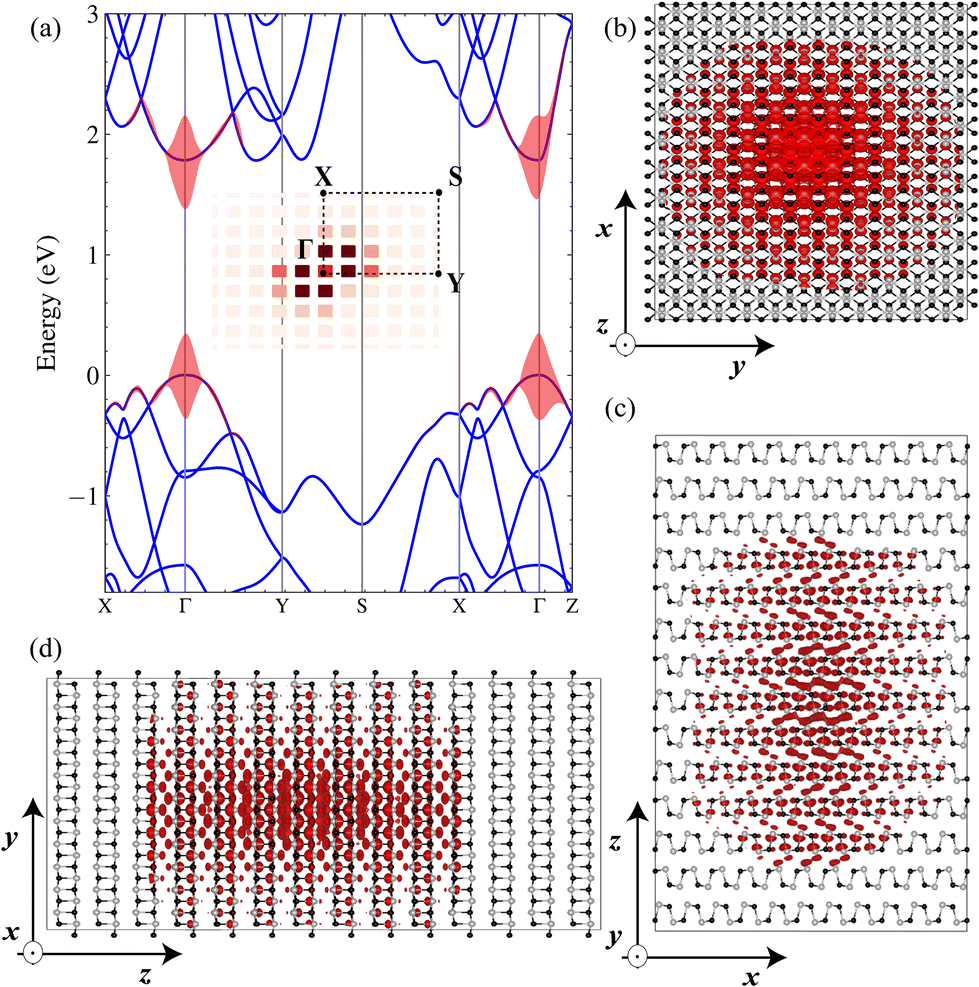 | ||
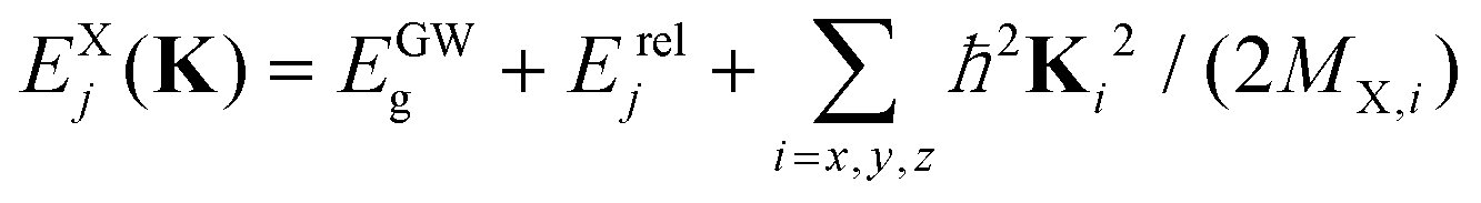
| Fig. 5 (a) Excitonic weights showing the most important electronic transitions along the high symmetry points of the BZ of GeS. Electronic transitions representing exciton weights are projected onto the ground-state electronic dispersion, which are depicted by the red shade. The colored inset shows the 2D projected exciton wavefunction distribution in k-space. Both the excitonic weights and k-space wavefunctions show that the first bright exciton originates from direct optical transitions in the vicinity of the Γ valley along the Γ X, Γ Y and Γ Z directions. (b, c and d) Normalized squared exciton wavefunction of first bright exciton in GeS using the BSE for incident light polarized along the AC direction. We fix the position of the hole near the S atom. Side view on the bottom and top view on the top. | ||
| Direction | k | State | S atom | Ge atom | |||||||||||
|---|---|---|---|---|---|---|---|---|---|---|---|---|---|---|---|
| s | pz | px | py | s | pz | px | py | dz2 | dxz | dyz | dx2−y2 | dxy | |||
| Γ | CBM | 7 | 0.9 | 8.4 | 0 | 7.9 | 64 | 6.8 | 0 | 0 | 0 | 0 | 0 | 0 | |
| VBM | 0.9 | 59.1 | 5 | 0 | 20.9 | 12.6 | 0.3 | 0 | 0 | 0 | 0 | 0 | 0 | ||
| AC | K 1 | CBM | 6.2 | 3 | 7.5 | 0.0 | 8.4 | 60.2 | 9.2 | 0 | 0 | 0 | 0 | 0 | 0 |
| VBM | 0.97 | 60 | 4.7 | 0.0 | 20 | 11.8 | 0.86 | 0.0 | 0 | 0 | 0 | 0 | 0 | ||
| ZZ | K 2 | CBM | 6.7 | 1.65 | 8 | 0.0 | 8.1 | 62 | 7.8 | 0.0 | 0 | 0 | 0 | 0 | 0 |
| VBM | 0.9 | 59.8 | 4.8 | 0 | 20 | 12 | 0.58 | 0.0 | 0 | 0 | 0 | 0 | 0 | ||
| AC | K 3 | CBM | 4.8 | 8 | 6.2 | 0.0 | 9 | 54.7 | 12 | 0.0 | 0 | 0 | 0 | 0 | 0 |
| VBM | 1.2 | 57.3 | 5.1 | 0.0 | 20.6 | 13 | 1.6 | 0.0 | 0 | 0 | 0 | 0 | 0 | ||
| AC | K 4 | CBM | 15.5 | 7 | 9.1 | 1.3 | 3.7 | 11.5 | 3 | 45.5 | 0 | 0 | 0 | 0 | 0 |
| VBM | 2.2 | 13 | 26.4 | 2 | 31.4 | 12.2 | 6.14 | 6.1 | 0 | 0 | 0 | 0 | 0 | ||
To investigate the exciton spatial extension, we plotted the relative e–h wavefunction in real space, see Fig. 5(b–d). This shows how these excitonic wavefunctions unfold over the real-space lattice. Indeed, we fixed the position of the hole on the top of the S atom (which contributes mainly to the top of the valence band, see section E of the ESI† for more information on the PDOS) separated by about 1 Å within the unit cell. Because the exciton wavefunction spreads over many unit lattices (more delocalized), they are more like Wannier-type excitons. In contrast to GeS, other anisotropic materials such as ReX2 due to their weak interlayer interactions, even for the bulk case, the exciton is mainly confined to a single layer (∼68%), leading to a relatively high binding energy of 120 meV and a small Bohr radius of 0.95 nm.62
In the following section, we used a semi-analytical theoretical model based on the EMA. In Table 3, we determined the effective masses (mν,ieff) of electrons (ν = e) and holes (ν = h) as well as the static dielectric constant (εi) in GeS for different crystal directions (i). These parameters can be inserted directly into the Schrödinger equation describing the interaction between e–h pairs. me,ieff and mh,ieff were calculated in terms of effective free electron mass units (m0) by means of a parabolic fitting of the valence and conduction band curvatures near the Γ k-point, see Fig. 3(a). mν,ieff and εi are strongly dependent on the crystal direction, revealing the influence of the crystal anisotropy on the optical properties of the excitonic states. The exciton reduced mass (μi = me,ieffmh,ieff/(me,ieff + me,ieff)) in the in-plane direction is larger compared to that in the out-of-plane direction, leading to a strong compression of the exciton Bohr radius (aib ∝ εiℏ2/e2μi) in the in-plane direction. As a result, our models will consider the exciton as an unconfined e–h pair, since the confinement potential is negligible compared to the Coulomb potential.
| m e,ieff (m0) | m h,ieff (m0) | μ i (m0) | ε i | |
|---|---|---|---|---|
| Γ–X | 0.845 | 1.011 | 0.46 | 10.94 |
| Γ–Y | 1.519 | 1.599 | 0.78 | 11.29 |
| Γ–Z | 0.019 | 0.101 | 0.016 | 10.72 |
4. Anisotropic Wannier exciton theory within the EMA
BSE demonstrates that the dominant contribution to the first bright exciton in GeS originates from the band states that lie in the vicinity of the Γ valley along the ΓX, ΓY, and ΓZ directions (see Fig. 5). We used this result to analyze the Schrödinger equation that describes the unconfined exciton in a pristine sample, taking into account the interaction between the e–h pair with anisotropic mν,ieff and εi. The Hamiltonian for modeling excitons in bulk semiconductors, along with the transformation to exciton coordinates, is described in section F of the ESI.† Using the relative r = (x, y, z) and center-of-mass (COM) RCM = (XCM, YCM, ZCM) coordinates, the resulting Schrödinger equation can be written as:64–66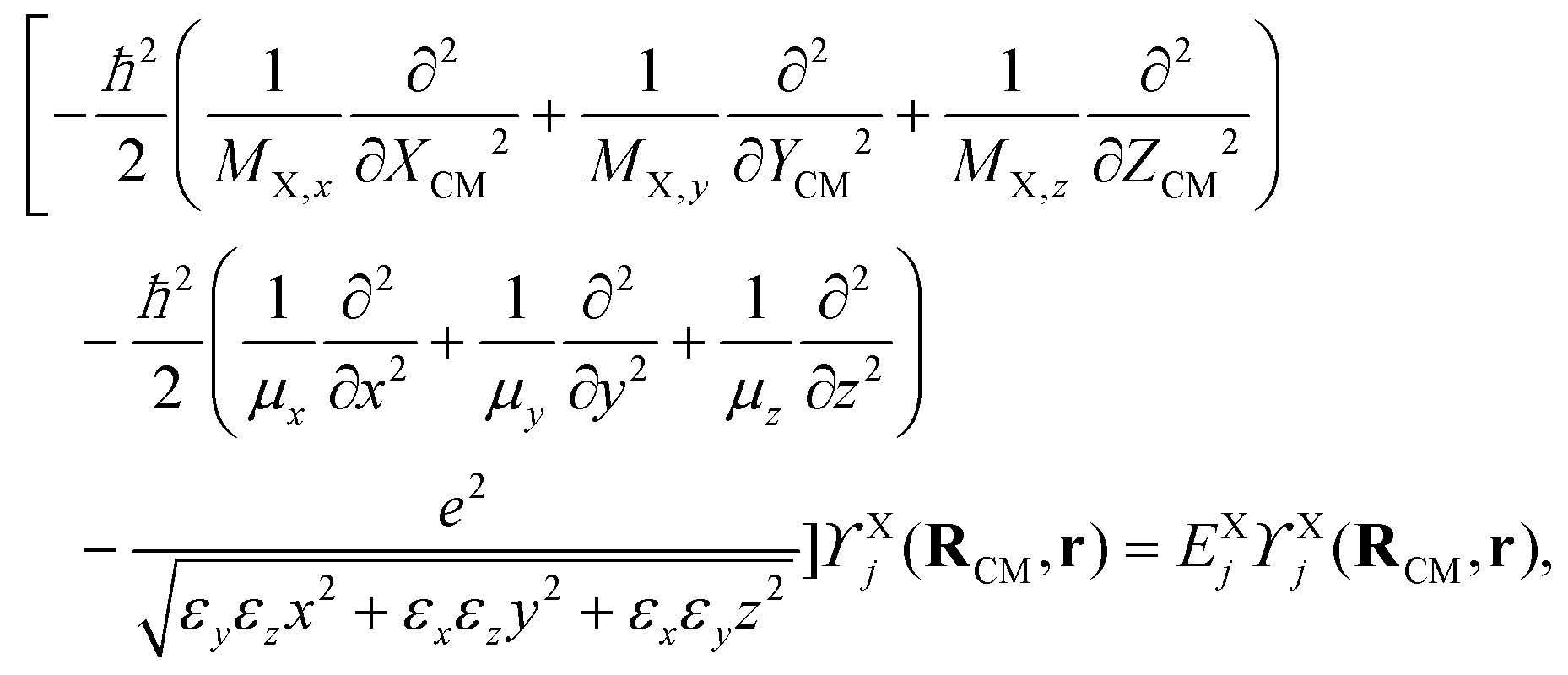 | (3) |
 and
and 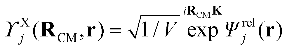 are the eigenenergy and eigenfunction solutions of the Schrödinger equation, respectively. Here, Erelj and Ψrelj(r) represent the eigenenergy and the eigenvector of the relative motion of the e–h pair. The COM wave vector is denoted by K = (Kx, Ky, Kz). The volume of a bulk semiconductor, V = NΩ, depends on the number of primitive cells (N) and the volume of the unit cell (Ω). To obtain the equation that describes Wannier excitons in an anisotropic medium, it is more convenient to transform from anisotropic masses to anisotropic potentials via the change of variables,
 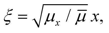 ,
, 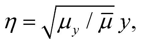 ,
, 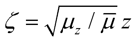 . Thus, the equation for the relative motion of the e–h pair with K = 0 reads
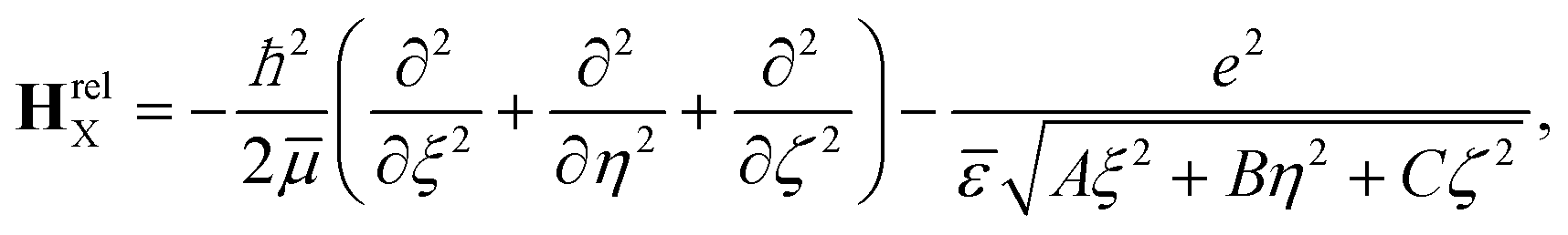 | (4) |
 ,
,  and
and  , assumed to be real and positive, estimate the degree of anisotropy.
  and
and  represent the average reduced mass and the dielectric constant, respectively. The problem is treated in spherical coordinates, where
  . This transformation integrates the anisotropy into the potential while maintaining the conventional form of an isotropic COM system with a reduced mass equal to
 ![[small mu, Greek, macron]](https://www.rsc.org/images/entities/i_char_e0cd.gif) . We utilized the new coordinate system for our calculations and only switch back to Cartesian coordinates x, y, and z when presenting the contour plots of the density wavefunction for clarity and interpretation. Expanding the relative wavefunction in a basis of 3D-hydrogenic wavefunction, Φn,,m(ρ, θ, φ), is convenient to solve eqn (4). We express the relative wavefunction
. We utilized the new coordinate system for our calculations and only switch back to Cartesian coordinates x, y, and z when presenting the contour plots of the density wavefunction for clarity and interpretation. Expanding the relative wavefunction in a basis of 3D-hydrogenic wavefunction, Φn,,m(ρ, θ, φ), is convenient to solve eqn (4). We express the relative wavefunction 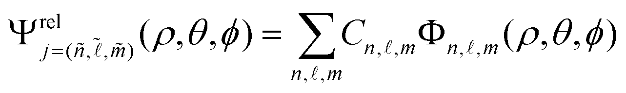 . Here, Cn,,m are expansion coefficients and Φn,,m(ρ,θ,φ) are the basis wavefunctions, where n, , and m represent the primary, azimuthal, and magnetic quantum numbers, respectively. The numerical diagonalization method was adopted for the resolution of eqn (4). In fact, the indices n, , and m refer to the dominant contributions of the coefficients Cn,,m to the relative excitonic wavefunction
  , corresponding to the coefficient of the highest weight. The matrix elements of the relative Hamiltonian can be written as:
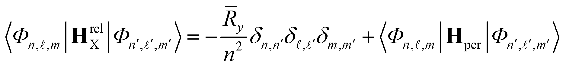 | (5) |
![[R with combining macron]](https://www.rsc.org/images/entities/i_char_0052_0304.gif) y = e2/(2
y = e2/(2![[small epsilon, Greek, macron]](https://www.rsc.org/images/entities/i_char_e0c6.gif) āb) is the 3D-effective Rydberg energy. āb = ℏ2/(e2) is the 3D-exciton effective Bohr radius and the perturbed Hamiltonian
āb) is the 3D-effective Rydberg energy. āb = ℏ2/(e2) is the 3D-exciton effective Bohr radius and the perturbed Hamiltonian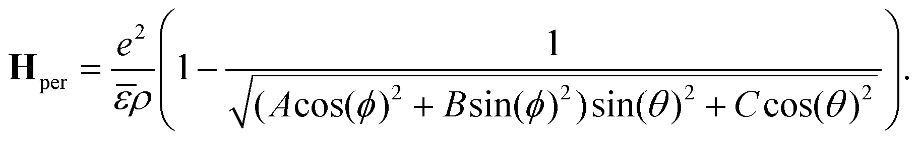 | (6) |
The perturbation reduces the symmetry of the system and, therefore, breaks the degeneracy of the excitonic state compared to the isotropic cases. For further information on the matrix elements and the excitonic Hamiltonian, see section F of the ESI.†
By the variation of the appropriate parameters (μi, εi and A, B, C), we can control the degree of anisotropy. To visualize the effects of anisotropy, Fig. 6(a) shows the first low-lying BEs of the relative excitonic states, 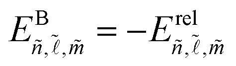 , obtained by numerical diagonalization of the matrix resulting from the projection of the Hamiltonian HrelX as given in eqn (4). To assign the exciton state according to its primary orbital character, we labelled them according to the (n, , m) component that produces the highest probability density
 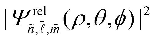 . For instance, the
 ![[1 with combining tilde]](https://www.rsc.org/images/entities/char_0031_0303.gif) s exciton is mainly dominated by the (1, 0, 0) component, while the (2, 1, 0) component largely contributes to the 2
s exciton is mainly dominated by the (1, 0, 0) component, while the (2, 1, 0) component largely contributes to the 2![[p with combining tilde]](https://www.rsc.org/images/entities/i_char_0070_0303.gif) 0 exciton and the (2, 1, ±1) component contributes significantly to the 2±1 exciton. In the bulk GeS case, as depicted in the right panel of Fig. 6, μi had a strong anisotropy along the direction i, while εi shows slight variations. In Fig. 6, we also studied two other different cases: (i) first, the middle panel represents a transversely isotropic system (such as an uniaxial system). We found that the in-plane reduced mass
0 exciton and the (2, 1, ±1) component contributes significantly to the 2±1 exciton. In the bulk GeS case, as depicted in the right panel of Fig. 6, μi had a strong anisotropy along the direction i, while εi shows slight variations. In Fig. 6, we also studied two other different cases: (i) first, the middle panel represents a transversely isotropic system (such as an uniaxial system). We found that the in-plane reduced mass  m0 ≠ μz. Similarly, the in-plane (
 ) and out-off-plane (εz) dielectric constants are also slightly different. (ii) Second, the left panel shows an isotropic system with a reduced mass of = 0.044m0 and a dielectric constant of = 10.98. The comparison between these two cases and the fully anisotropic one (GeS) shows that the anisotropy strongly affects the degeneracy of the excitonic states. In fact, for an isotropic system, the results of the symmetric Coulomb potential are found to follow −y/n2, where the states are (2n + 1)-fold degenerate. In contrast to 3D hydrogenic-like models, the anisotropy clearly lifts the degeneracy of the different excited excitonic states. Additionally, the excitonic states are apparent in an anomalous energy level order of the azimuthal quantum number
  and the magnetic quantum number
 ![[m with combining tilde]](https://www.rsc.org/images/entities/i_char_006d_0303.gif) . For example, the 2
. For example, the 2![[p with combining tilde]](https://www.rsc.org/images/entities/char_0070_0303.gif) +1 states lay energetically below the 2
+1 states lay energetically below the 2![[s with combining tilde]](https://www.rsc.org/images/entities/char_0073_0303.gif) state, due to the asymmetry caused by the effective mass and the dielectric constant anisotropy. This means that the radial and angular dependencies in the Wannier equation can be separated. However, for bulk GeS, the anisotropy reduces the symmetry of the system. In this case, the radial and angular degrees of freedom are coupled, which lifts the degeneracy. Interestingly, a two-fold degeneracy is found for transverse isotropy, so that for the same
state, due to the asymmetry caused by the effective mass and the dielectric constant anisotropy. This means that the radial and angular dependencies in the Wannier equation can be separated. However, for bulk GeS, the anisotropy reduces the symmetry of the system. In this case, the radial and angular degrees of freedom are coupled, which lifts the degeneracy. Interestingly, a two-fold degeneracy is found for transverse isotropy, so that for the same  , positive and negative values of the magnetic quantum number lead to the same energy. This degeneracy is removed in GeS, producing, for example, a 0.2 meV separation between 2+1 and 2−1 states. In the transverse anisotropy case, the exciton Hamiltonian exhibits a uniaxial symmetry. Consequently, it is possible to diagonalize the matrices separately for even and odd and for different m. In the angular momentum space, this special characteristic results in a block-diagonal eigenvalue problem. In contrast, for GeS, the anisotropy mixes states with the same but different m.
 | ||
| Fig. 6 (a) BE of exciton states, showcasing the transition from isotropic to anisotropic cases across three panels. Each panel is further subdivided into columns, with each column denoting a magnetic quantum number m (ranging from 0, ±1, and ±2, from left to right), while the different line colors represent states. The left panel illustrates the isotropic case with average values of the reduced exciton mass and the dielectric constant . In the middle panel, we consider the transversely isotropic scenario, where μ‖ ≠ μz and ε‖ ≠ εz. The right panel showcases the BE of exciton states in bulk GeS. (b–g) Comparison of the probability density, which represents the squared modulus of the corrected wavefunctions for the ground excitonic state projected in real space, presented in contour plots. These plots are shown in the (x, y) plane for figures (b, d and f) and in the (x, z) plane for figures (c, e and g). The unit of Bohr radius is used for all three cases. The figures correspond to the isotropic, transversely isotropic, and anisotropic cases, from top to bottom respectively. | ||
In addition to lifting the degeneracy, we can clearly notice that the exciton BE strongly depends on the reduced mass and the dielectric constant and hence on the anisotropic parameters A, B, and C. Strong anisotropy (A ≠ B ≠ C) leads to an increase (EB/y = 1.5) in the exciton BE compared to the isotropic case (A = B = C). In the EMA, we found that the s-exciton BE and Bohr radius of the bulk GeS were ∼7.6 meV and 13 nm, respectively. This is consistent with the BSE method, which indicates that the exciton BE is ∼10 meV. In fact, the small BE (largest Bohr radius) is due to the highest effective dielectric function and the smaller reduced mass , where the reduced mass out-of-plane is significantly smaller than those in-plane. These values account for the swift disappearance of exciton emission at high temperatures, since their magnitudes are lower than the thermal energy (kBT). In fact, in section A of the ESI† using temperature-dependent PL, we estimated the quenching of the exciton emission at a temperature of 130 K under 2.41 eV excitation, compared to 190 K under 1.88 eV resonant excitation.
To better understand the impact of anisotropy on exciton wavefunctions, we compared the probability densities (squared moduli of the excitonic wavefunctions) for the ground-state excitonic wavefunction s for the three previous cases in Fig. 6(b–g). The isotropic case produces the well-known hydrogen-like wavefunctions. For the transversal isotropic case, as expected, the excitonic wavefunction for the in-plane compound has a spherical symmetry, while the orbital becomes a disk stretched along the z-direction, since the reduced mass in the z-direction is much smaller than the average in-plane reduced mass. For GeS, the anisotropy modifies the ground state from a spherically symmetric s (isotropic) to a squeezed wavefunction with a slightly peanut shape. In fact, we found that the s state stretched in the three directions; however, the distortions (squeezing) are more significant in the out-of-plane direction due to the heavier mass of this direction. The smaller area across which the probability density extends in the in-plane direction for the anisotropic case as compared to the isotopic one is due to the higher BE, which leads to more localized wavefunctions.
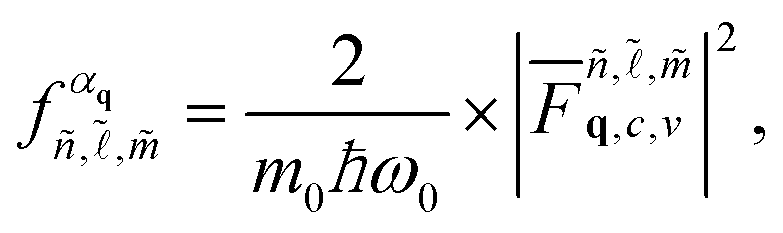
Fig. 7(b) illustrates the impact of anisotropic parameters (A, B, C) on the ground state (s) and highlights the strong dependence of the exciton energy on the degree of anisotropy. By adjusting these parameters, we can shift from the strong anisotropy case to the isotropy one. In fact, depending on the values of A and B, we found three limiting regimes. If A = B = C = 1, eqn (4) and (5) become the well-known equation for the isotropic case, whose eigenvalues are −y/n2, with the well-known degree of degeneracy n2 so that EB1s = y, as clearly shown in Fig. 7(c). Then, with the decrease of A and B, the degree of perturbation induced by the anisotropy increases, leading to an increase in the exciton BE. Indeed, for A = B ≥ 0.1, the excitonic ground state tends to the well-known 2D-hydrogenic energy  due to the asymmetry in the Coulomb potential caused by the strong perturbation induced by the anisotropy in this regime. Interestingly, for A = B ≥ 1, we found that the 1-exciton energy is lower than the Rydberg energy
 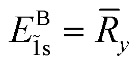 .
.
 | ||
| Fig. 7 Anisotropy effect on OS for low-lying exciton states in GeS. (a) Normalized OS for the first low-lying ñs state for different cases. (b) s-exciton BE as a function of anisotropy parameters. The plot presents three critical regions (isotropic, weak anisotropic, and strong anisotropic), which are separated by a dashed cyan line. (c) Theoretical prediction of the angle-resolved PL spectrum for GeS. (d) Direct comparison between experimental and theoretical PL for low-lying exciton states. | ||
From the knowledge of the exciton energies and wavefunctions as functions of the anisotropic parameters, we can compute the OS and hence the PL signal for these exciton states. Indeed, the OS is a dimensionless quantity that gives the relative strength of a particular optical transition. Here, we consider only the most common case of direct allowed optical transitions between the valence and conduction bands. For instance, the OS of the optical interband transition for exciton states is
 . The quantity
 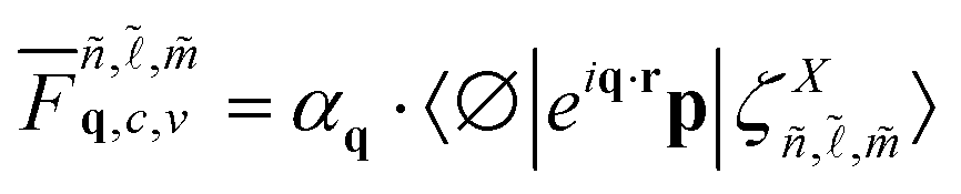 is the OME between the crystal ground state |∅〉 and the excited states
  corresponding to the direct exciton in bulk GeS. Here,
  , and αq denotes the photon polarization unit vector. For the scenario of unconfined exciton COM motion in bulk GeS, the OS is expressed as follows (see section F in the ESI† for more details)67
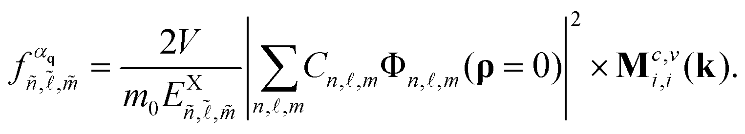 | (7) |
The OME and the relative wavefunction give rise to different types of selection rules. Indeed, only allowed transitions occur within the excitonic state wherein the relative wavefunction 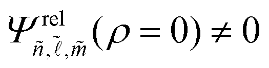 . For the OME, the selection rules come mainly from the interband coupling term, which depends on the nature of the Bloch function.
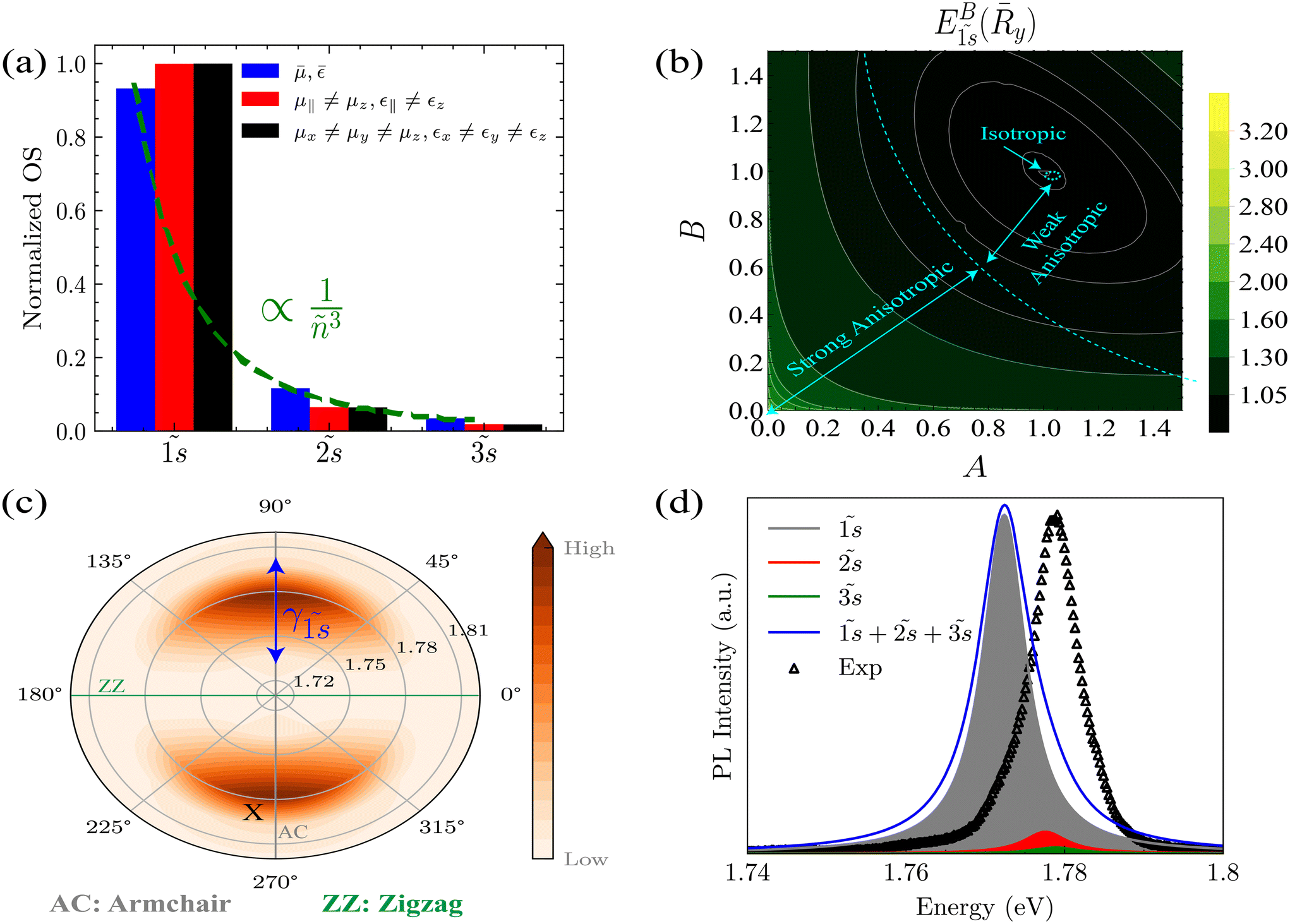
Fig. 7(a) presents the calculated normalized OS of the three low-lying s-exciton states 1, 2, and 3 in bulk GeS (black line). For comparison, we also plotted the OS for the isotropic (blue line) and transversal isotropic (red line) cases. It is seen that the OS decay ratio in the anisotropic case shows an anomalous behavior compared to that in the isotopic case. In GeS, the intensity ratio 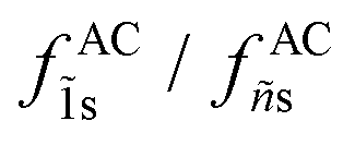 exhibits different values compared to a bare isotropic hydrogen-like Coulomb potential, where the exciton OS of states ñs decays as
 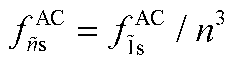 . Specifically, the ratio is approximately 15 for s/
![[2 with combining tilde]](https://www.rsc.org/images/entities/char_0032_0303.gif) s and 55 for s/
s and 55 for s/![[3 with combining tilde]](https://www.rsc.org/images/entities/char_0033_0303.gif) s, while it is equal to 8 and 27, respectively, in the isotropic case. This finding is consistent with the results reported by T. Shubina et al. for InSe.68 Indeed, this difference is due to the fact that, in contrast to the isotropic case, the perturbation induced by anisotropy generates linear combinations of basis functions, so different orbitals with different weights, Cn,,m, contribute in each anisotropic excitonic transition. Therefore, the s-, p- and even d-state shell excitons are mixed due to the reduction of symmetry induced by the anisotropy of GeS. This mixing makes the p-shell states optically active. Hence, both s-shell and p-shell excitons are active in both one- and two-photon processes, providing an efficient mechanism of second-harmonic generation. The discernible characteristic may be observed through the perturbed matrix elements. Moreover, this illustrates that states with different angular momentum components are indistinguishable in GeS, which well describes the mixing of excitonic states with different parities, particularly the s-shell and p-shell states. These non-linear contributions are similar to those related to the magneto-Stark effect or the electric-field-induced mixing of excitons in ZnO69 and GaAs.70 The non-linear contributions to the exciton emission are beyond the scope of this work, as the one-photon emission is investigated. In addition, we found that the ñs-state BEs for the transversal isotropic and full anisotropic cases are almost similar. This is also shown in Fig. 6, in which the exciton BEs of the ñs-state for these two cases are almost equal. In fact, due to the effective light mass along the z direction compared to the in-plane effective mass, the total effective mass in the anisotropic case () is almost equal to the transversal isotopic case (μ‖), which produces a comparable Rydberg energy (y) and Bohr radius (āb) in both cases.
s, while it is equal to 8 and 27, respectively, in the isotropic case. This finding is consistent with the results reported by T. Shubina et al. for InSe.68 Indeed, this difference is due to the fact that, in contrast to the isotropic case, the perturbation induced by anisotropy generates linear combinations of basis functions, so different orbitals with different weights, Cn,,m, contribute in each anisotropic excitonic transition. Therefore, the s-, p- and even d-state shell excitons are mixed due to the reduction of symmetry induced by the anisotropy of GeS. This mixing makes the p-shell states optically active. Hence, both s-shell and p-shell excitons are active in both one- and two-photon processes, providing an efficient mechanism of second-harmonic generation. The discernible characteristic may be observed through the perturbed matrix elements. Moreover, this illustrates that states with different angular momentum components are indistinguishable in GeS, which well describes the mixing of excitonic states with different parities, particularly the s-shell and p-shell states. These non-linear contributions are similar to those related to the magneto-Stark effect or the electric-field-induced mixing of excitons in ZnO69 and GaAs.70 The non-linear contributions to the exciton emission are beyond the scope of this work, as the one-photon emission is investigated. In addition, we found that the ñs-state BEs for the transversal isotropic and full anisotropic cases are almost similar. This is also shown in Fig. 6, in which the exciton BEs of the ñs-state for these two cases are almost equal. In fact, due to the effective light mass along the z direction compared to the in-plane effective mass, the total effective mass in the anisotropic case () is almost equal to the transversal isotopic case (μ‖), which produces a comparable Rydberg energy (y) and Bohr radius (āb) in both cases.
The OS per unit volume can be related to the probability of emission of a photon over all the photon modes using the following formula:
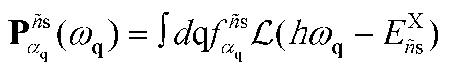 | (8) |
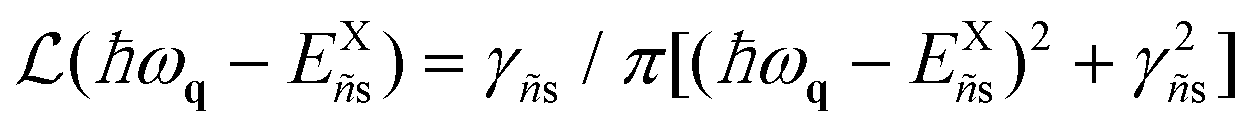 expresses the energy conservation taking into account the state of the linewidth broadening extracted from our experiment, γs = 8 meV. Notably, the OS of exciton states is generally different between one- and two-photon processes. In Fig. 7(d), we plotted the PL spectra for different excitonic states, and in the same plot we show the experimental PL spectrum of the free exciton at low temperature. We found that the exciton ground state s located at around 1.772 eV dominates the PL spectrum, which is expected since it has the largest OS. When comparing our experimental results, it is evident that the excited excitonic states, such as s and s, are not clearly visible in our measurements. This is due to different factors: (i) the largest linewidth broadening (γs), which is significantly greater than the energy separation between different excitonic states (
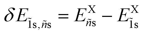 ) and (ii) the value of the OS (which is directly proportional to the PL intensity) that corresponds to the excited exciton ñs states is lower than the s state. Thus, the nearly energetic ñs states overlap and assemble into a single peak in the PL spectra, which appears to be broadened and asymmetric with a lower slope on the lower-energy side. It is important to note that this peak's asymmetry may also be due to phonon-assisted processes.71
Using eqn (8), we calculated the angle-resolved PL at low temperature in Fig. 7(d). The PL signal is strongly dependent on the polarization angle. In fact, the exciton signal is maximum along the AC direction, then the signal intensity decreases until it disappears in the ZZ direction. This demonstrates the anisotropic optical signature in GeS, and agrees well with the experimental results in Fig. 1.
Our experimental results reveal the existence of multiple emission peaks at low temperature in GeS encapsulated with h-BN, in addition to the free neutral exciton peak, these peaks are located in the energy range of approximately 60–100 meV below the neutral exciton. Despite thorough investigations, the nature of these low-energy emission remains unknown, both from theoretical and experimental perspectives. During this study, to identify these peaks, we qualitatively studied different scenarios, including biexciton, optical phonon-assisted exciton recombination, emission of charged excitons (trions) and their fine structure, and exciton plus a localized exciton. More details about the nature of these peaks can be found in sections A and B of the ESI;† however, a deep quantitative study of these low-energy emissions is beyond the scope of the present paper.
5. Conclusions
Anisotropy of the low-symmetry orthorhombic crystal structure of GeS offers possibilities for the manipulation of physical properties along different crystal directions. We presented a detailed study of the anisotropic properties of GeS using temperature- and polarization-dependent PL techniques supported by ab initio calculations. Temperature-dependent PL experiments enabled us to investigate the excitonic impact on the optical properties of GeS, whilst polarization-dependent PL measurements revealed the anisotropic nature of the material. Ab initio calculations were used to theoretically predict the electronic BS and optical properties of GeS and to interpret the experimental results. By applying both the IPA and GW + BSE methods, we calculated the dielectric functions and showed that including exciton effects through the BSE method modifies the optical absorption spectra in bulk GeS. Using the EMA, we showed that compared to an isotropic system, the anisotropy in GeS breaks the degeneracy, causes mixing of states with the same quantum number but different orbital and angular quantum numbers, and increases the BE. We also found a relatively low BE, on the order of ∼10 meV, and a quite large exciton Bohr radius, on the order of 13 nm, which explains the observed rapid decrease in the exciton peak as the temperature increases. This result provides an essential understanding of the complexities of anisotropic materials and may have ramifications for the design of certain technological applications.6. Methods
6.1. Sample
The studied sample is composed of a thin layer of GeS, characterized by a thickness of about 60 nm, encapsulated in h-BN flakes and placed on a Si/SiO2 substrate. The GeS crystal, which was used for the preparation of the investigated sample, was purchased from HQ graphene. Thin GeS flakes were directly exfoliated on a 285 nm SiO2/Si substrate in an inert gas glovebox (O2 < 1 ppm, H2O < 1 ppm). Then we used a poly(bisphenol A carbonate)/polydimethylsiloxane stamp on a glass slide to pick up top h-BN, thin flakes of GeS, and bottom h-BN at 80 °C with the assistance of the transfer stage in the glove box. Finally, the stack was released on a Si/SiO2 substrate. The thicknesses of the GeS flakes were first identified by optical contrast and then measured more precisely with an atomic force microscope.6.2. Experimental techniques
PL spectra were recorded at different illumination wavelengths with a series of continuous wave (CW) laser diodes: λ = 488 nm (2.54 eV), λ = 515 nm (2.41 eV), λ = 561 nm (2.21 eV), λ = 633 nm (1.96 eV), and λ = 660 nm (1.88 eV). PLE experiment was carried out using a supercontinuum light source coupled with a monochromator as an excitation source. For the RC studies, the only difference in the experimental setup with respect to the one used to record the PL and PLE signals concerned the excitation source, which was replaced by a tungsten halogen lamp. The studied samples were placed on a cold finger in a continuous-flow cryostat mounted on x–y motorized positioners. The excitation light was focused by means of a 100× long working distance objective with a 0.55 numerical aperture that produced a spot of about 1/4 μm diameter in the PL/RC measurements. The signal was collected via the same microscope objective, sent through a 0.75 m monochromator, and then detected using a cooled charge-coupled device camera cooled with liquid nitrogen. The excitation power focused on the sample was kept at 100 μW during all measurements to avoid local heating. Polarization-resolved PL and RC spectra were recorded using a motorized half-wave plate mounted on top of the microscope objective and a fixed linear polarizer placed in the detection path, which provides simultaneous rotation of the co-linearly polarized excitation light and detected signal.6.3. Computational details
Author contributions
Z. C. and M. K. fabricated the samples; K. W. and T. T. provided the hBN crystals; M. A., N. Z., A.B., and M. R. M. carried out the experiments; N. Z. and M. R. M performed the experimental data analysis; M. A. and S. A. performed the theoretical study; M. A. carried out DFT, GW, BSE and EMA calculations; M. R. M. designed the project; M. A., N. Z., S. A., S. J, and M. R. M. prepared the manuscript with contribution from all other co-authors.Conflicts of interest
There are no conflicts to declare.Acknowledgements
This work was supported by the National Science Centre, Poland (Grant No. 2017/27/B/ST3/00205 and 2018/31/B/ST3/02111), the Ministry of Education (Singapore) through the Research Centre of Excellence Program (grant EDUN C-33-18-279-V12, I-FIM) and under its Academic Research Fund Tier 2 (MOE-T2EP50122-0012), and the Air Force Office of Scientific Research and the Office of Naval Research Global under award number FA8655-21-1-7026. K. W. and T. T. acknowledge the support from the JSPS KAKENHI (Grant Numbers 20H00354 and 23H02052) and World Premier International Research Center Initiative (WPI), MEXT, Japan.References
- R. Mas-Balleste, C. Gomez-Navarro, J. Gomez-Herrero and F. Zamora, Nanoscale, 2011, 3, 20–30 RSC.
- G. R. Bhimanapati, Z. Lin, V. Meunier, Y. Jung, J. Cha, S. Das, D. Xiao, Y. Son, M. S. Strano and V. R. Cooper, et al. , ACS Nano, 2015, 9, 11509–11539 CrossRef CAS PubMed.
- D. Jariwala, V. K. Sangwan, L. J. Lauhon, T. J. Marks and M. C. Hersam, ACS Nano, 2014, 8, 1102–1120 CrossRef CAS PubMed.
- Q. H. Wang, K. Kalantar-Zadeh, A. Kis, J. N. Coleman and M. S. Strano, Nat. Nanotechnol., 2012, 7, 699–712 CrossRef CAS PubMed.
- Z. Wu, Y. Lyu, Y. Zhang, R. Ding, B. Zheng, Z. Yang, S. P. Lau, X. H. Chen and J. Hao, Nat. Mater., 2021, 20, 1203–1209 CrossRef CAS PubMed.
- M. R. Molas, Ł. Macewicz, A. Wieloszyńska, P. Jakóbczyk, A. Wysmołek, R. Bogdanowicz and J. B. Jasinski, npj 2D Mater. Appl., 2021, 5, 83 CrossRef CAS.
- H. Liu, A. T. Neal, Z. Zhu, Z. Luo, X. Xu, D. Tománek and P. D. Ye, ACS Nano, 2014, 8, 4033–4041 CrossRef CAS PubMed.
- J. Qiao, X. Kong, Z.-X. Hu, F. Yang and W. Ji, Nat. Commun., 2014, 5, 4475 CrossRef CAS PubMed.
- V. Podzorov, M. Gershenson, C. Kloc, R. Zeis and E. Bucher, Appl. Phys. Lett., 2004, 84, 3301–3303 CrossRef CAS.
- M. M. Ugeda, A. J. Bradley, S.-F. Shi, F. H. Da Jornada, Y. Zhang, D. Y. Qiu, W. Ruan, S.-K. Mo, Z. Hussain and Z.-X. Shen, et al. , Nat. Mater., 2014, 13, 1091–1095 CrossRef CAS PubMed.
- G. Zhang, A. Chaves, S. Huang, F. Wang, Q. Xing, T. Low and H. Yan, Sci. Adv., 2018, 4, eaap9977 CrossRef PubMed.
- J. Henriques and N. Peres, Phys. Rev. B, 2020, 101, 035406 CrossRef CAS.
- M. Kim, H.-G. Kim, S. Park, J. S. Kim, H. J. Choi, S. Im, H. Lee, T. Kim and Y. Yi, Angew. Chem., Int. Ed., 2019, 58, 3754–3758 CrossRef CAS PubMed.
- Q. Li, Q. Zhou, L. Shi, Q. Chen and J. Wang, J. Mater. Chem. A, 2019, 7, 4291–4312 RSC.
- K. Sadki, S. Sadki and L. B. Drissi, J. Phys. Chem. Solids, 2019, 130, 13–18 CrossRef CAS.
- L. C. Gomes and A. Carvalho, Phys. Rev. B: Condens. Matter Mater. Phys., 2015, 92, 085406 CrossRef.
- X. Lv, W. Wei, Q. Sun, F. Li, B. Huang and Y. Dai, Appl. Catal., B, 2017, 217, 275–284 CrossRef CAS.
- L. Wu, Z. Xie, L. Lu, J. Zhao, Y. Wang, X. Jiang, Y. Ge, F. Zhang, S. Lu and Z. Guo, et al. , Adv. Opt. Mater., 2018, 6, 1700985 CrossRef.
- Y. Yang, S.-C. Liu, Z. Li, D.-J. Xue and J.-S. Hu, Chem. Commun., 2021, 57, 565–575 RSC.
- N. Latiff, W. Z. Teo, Z. Sofer, Š. Huber, A. C. Fisher and M. Pumera, RSC Adv., 2015, 5, 67485–67492 RSC.
- H. Wiedemeier and P. Siemers, Z. Anorg. Allg. Chem., 1977, 431, 299–304 CrossRef CAS.
- J. Liu and S. T. Pantelides, Appl. Phys. Express, 2018, 11, 101301 CrossRef.
- M. Feng, S.-C. Liu, L. Hu, J. Wu, X. Liu, D.-J. Xue, J.-S. Hu and L.-J. Wan, J. Am. Chem. Soc., 2021, 143, 9664–9671 CrossRef CAS PubMed.
- N. Zawadzka, Ł. Kipczak, T. Woźniak, K. Olkowska-Pucko, M. Grzeszczyk, A. Babiński and M. R. Molas, Nanomaterials, 2021, 11, 3109 CrossRef CAS PubMed.
- R. K. Ulaganathan, Y.-Y. Lu, C.-J. Kuo, S. R. Tamalampudi, R. Sankar, K. M. Boopathi, A. Anand, K. Yadav, R. J. Mathew and C.-R. Liu, et al. , Nanoscale, 2016, 8, 2284–2292 RSC.
- X. Wang, J. Tan, C. Han, J.-J. Wang, L. Lu, H. Du, C.-L. Jia, V. L. Deringer, J. Zhou and W. Zhang, ACS Nano, 2020, 14, 4456–4462 CrossRef CAS PubMed.
- C. Lan, C. Li, Y. Yin, H. Guo and S. Wang, J. Mater. Chem. C, 2015, 3, 8074–8079 RSC.
- M. Taniguchi, R. Johnson, J. Ghijsen and M. Cardona, Phys. Rev. B: Condens. Matter Mater. Phys., 1990, 42, 3634 CrossRef CAS PubMed.
- A. Tołłoczko, R. Oliva, T. Woźniak, J. Kopaczek, P. Scharoch and R. Kudrawiec, Mater. Adv., 2020, 1, 1886–1894 RSC.
- L.-D. Zhao, S.-H. Lo, Y. Zhang, H. Sun, G. Tan, C. Uher, C. Wolverton, V. P. Dravid and M. G. Kanatzidis, Nature, 2014, 508, 373–377 CrossRef CAS PubMed.
- S.-D. Guo and Y.-H. Wang, J. Appl. Phys., 2017, 121, 034302 CrossRef.
- W. Senske, R. Street, A. Nowitzki and P. Wiesner, J. Lumin., 1978, 16, 343–352 CrossRef CAS.
- J. Wiley, D. Thomas, E. Schönherr and A. Breitschwerdt, J. Phys. Chem. Solids, 1980, 41, 801–807 CrossRef CAS.
- A. El-Bakkali, S. Sadki, L. B. Drissi and F. Djeffal, Phys. E, 2021, 133, 114791 CrossRef CAS.
- D. Tan, H. E. Lim, F. Wang, N. B. Mohamed, S. Mouri, W. Zhang, Y. Miyauchi, M. Ohfuchi and K. Matsuda, Nano Res., 2017, 10, 546–555 CrossRef CAS.
- P. Le, C. V. Nguyen, D. V. Thuan, T. V. Vu, V. Ilyasov, N. Poklonski, H. V. Phuc, I. Ershov, G. Geguzina and N. V. Hieu, et al. , J. Electron. Mater., 2019, 48, 2902–2909 CrossRef CAS.
- R. Fei, W. Li, J. Li and L. Yang, Appl. Phys. Lett., 2015, 107, 173104 CrossRef.
- G. Qin, Z. Qin, W.-Z. Fang, L.-C. Zhang, S.-Y. Yue, Q.-B. Yan, M. Hu and G. Su, Nanoscale, 2016, 8, 11306–11319 RSC.
- M. Wu and X. C. Zeng, Nano Lett., 2016, 16, 3236–3241 CrossRef CAS.
- C.-H. Ho and J.-X. Li, Adv. Opt. Mater., 2017, 5, 1600814 CrossRef.
- D. Tan, W. Zhang, X. Wang, S. Koirala, Y. Miyauchi and K. Matsuda, Nanoscale, 2017, 9, 12425–12431 RSC.
- A. Shafique and Y.-H. Shin, Sci. Rep., 2017, 7, 506 CrossRef PubMed.
- R. Oliva, T. Woźniak, F. Dybala, A. Tołłoczko, J. Kopaczek, P. Scharoch and R. Kudrawiec, Phys. Rev. B, 2020, 101, 235205 CrossRef CAS.
- M. Yang, S. Cao, Q. You, L.-B. Shi and P. Qian, Phys. E, 2020, 118, 113877 CrossRef CAS.
- F. Li, X. Liu, Y. Wang and Y. Li, J. Mater. Chem. C, 2016, 4, 2155–2159 RSC.
- E. E. Salpeter and H. A. Bethe, Phys. Rev., 1951, 84, 1232–1242 CrossRef.
- M. Rohlfing and S. G. Louie, Phys. Rev. B: Condens. Matter Mater. Phys., 2000, 62, 4927–4944 CrossRef CAS.
- F. Cadiz, E. Courtade, C. Robert, G. Wang, Y. Shen, H. Cai, T. Taniguchi, K. Watanabe, H. Carrere, D. Lagarde, M. Manca, T. Amand, P. Renucci, S. Tongay, X. Marie and B. Urbaszek, Phys. Rev. X, 2017, 7, 021026 Search PubMed.
- K. P. O'Donnell and X. Chen, Appl. Phys. Lett., 1991, 58, 2924–2926 CrossRef.
- S. Rudin, T. L. Reinecke and B. Segall, Phys. Rev. B: Condens. Matter Mater. Phys., 1990, 42, 11218–11231 CrossRef CAS PubMed.
- G. Ding, G. Gao and K. Yao, Sci. Rep., 2015, 5, 9567 CrossRef CAS PubMed.
- S. Hao, F. Shi, V. P. Dravid, M. G. Kanatzidis and C. Wolverton, Chem. Mater., 2016, 28, 3218–3226 CrossRef CAS.
- T. Grandke and L. Ley, Phys. Rev. B: Solid State, 1977, 16, 832–842 CrossRef CAS.
- J. Wiley, A. Breitschwerdt and E. Schönherr, Solid State Commun., 1975, 17, 355–359 CrossRef CAS.
- T. Yabumoto, J. Phys. Soc. Jpn., 1958, 13, 559–562 CrossRef CAS.
- S. Postorino, J. Sun, S. Fiedler, L. O. Lee Cheong Lem, M. Palummo and L. Camilli, Materials, 2020, 13, 3568 CrossRef CAS PubMed.
- B. D. Malone and E. Kaxiras, Phys. Rev. B: Condens. Matter Mater. Phys., 2013, 87, 245312 CrossRef.
- V. Tran, R. Soklaski, Y. Liang and L. Yang, Phys. Rev. B: Condens. Matter Mater. Phys., 2014, 89, 235319 CrossRef.
- T. Cheiwchanchamnangij and W. R. L. Lambrecht, Phys. Rev. B: Condens. Matter Mater. Phys., 2012, 85, 205302 CrossRef.
- W. Shan, B. D. Little, A. J. Fischer, J. J. Song, B. Goldenberg, W. G. Perry, M. D. Bremser and R. F. Davis, Phys. Rev. B: Condens. Matter Mater. Phys., 1996, 54, 16369–16372 CrossRef CAS PubMed.
- P. Belov and E. Khramtsov, J. Phys.: Conf. Ser., 2017, 012018 CrossRef.
- A. Arora, J. Noky, M. Druppel, B. Jariwala, T. Deilmann, R. Schneider, R. Schmidt, O. Del Pozo-Zamudio, T. Stiehm and A. Bhattacharya, et al. , Nano Lett., 2017, 17, 3202–3207 CrossRef CAS PubMed.
- C. Ho, Y. Huang, K.-K. Tiong and P. Liao, Phys. Rev. B: Condens. Matter Mater. Phys., 1998, 58, 16130 CrossRef CAS.
- T. Kuzuba and K. Era, J. Phys. Soc. Jpn., 1976, 40, 134–139 CrossRef CAS.
- A. Baldereschi and M. Diaz, Il Nuovo Cimento B, 1970, 68, 217–229 CrossRef CAS.
- G. Dresselhaus, J. Phys. Chem. Solids, 1956, 1, 14–22 CrossRef.
- M. Shinada and S. Sugano, J. Phys. Soc. Jpn., 1966, 21, 1936–1946 CrossRef CAS.
- T. V. Shubina, W. Desrat, M. Moret, A. Tiberj, O. Briot, V. Y. Davydov, A. V. Platonov, M. A. Semina and B. Gil, Nat. Commun., 2019, 10, 3479 CrossRef CAS PubMed.
- M. Lafrentz, D. Brunne, B. Kaminski, V. V. Pavlov, A. V. Rodina, R. V. Pisarev, D. R. Yakovlev, A. Bakin and M. Bayer, Phys. Rev. Lett., 2013, 110, 116402 CrossRef CAS PubMed.
- D. Brunne, M. Lafrentz, V. V. Pavlov, R. V. Pisarev, A. V. Rodina, D. R. Yakovlev and M. Bayer, Phys. Rev. B: Condens. Matter Mater. Phys., 2015, 92, 085202 CrossRef.
- V. Funk, K. Wagner, E. Wietek, J. D. Ziegler, J. Förste, J. Lindlau, M. Förg, K. Watanabe, T. Taniguchi, A. Chernikov and A. Högele, Phys. Rev. Res., 2021, 3(4), L042019 CrossRef CAS.
- P. Giannozzi, S. Baroni, N. Bonini, M. Calandra, R. Car, C. Cavazzoni, D. Ceresoli, G. L. Chiarotti, M. Cococcioni, I. Dabo, A. D. Corso, S. de Gironcoli, S. Fabris, G. Fratesi, R. Gebauer, U. Gerstmann, C. Gougoussis, A. Kokalj, M. Lazzeri, L. Martin-Samos, N. Marzari, F. Mauri, R. Mazzarello, S. Paolini, A. Pasquarello, L. Paulatto, C. Sbraccia, S. Scandolo, G. Sclauzero, A. P. Seitsonen, A. Smogunov, P. Umari and R. M. Wentzcovitch, J. Phys.: Condens. Matter, 2009, 21, 395502 CrossRef PubMed.
- P. Giannozzi, O. Andreussi, T. Brumme, O. Bunau, M. B. Nardelli, M. Calandra, R. Car, C. Cavazzoni, D. Ceresoli, M. Cococcioni, N. Colonna, I. Carnimeo, A. D. Corso, S. de Gironcoli, P. Delugas, R. A. DiStasio, A. Ferretti, A. Floris, G. Fratesi, G. Fugallo, R. Gebauer, U. Gerstmann, F. Giustino, T. Gorni, J. Jia, M. Kawamura, H.-Y. Ko, A. Kokalj, E. Kucukkbenli, M. Lazzeri, M. Marsili, N. Marzari, F. Mauri, N. L. Nguyen, H.-V. Nguyen, A. O. de-la Roza, L. Paulatto, S. Poncé, D. Rocca, R. Sabatini, B. Santra, M. Schlipf, A. P. Seitsonen, A. Smogunov, I. Timrov, T. Thonhauser, P. Umari, N. Vast, X. Wu and S. Baroni, J. Phys.: Condens. Matter, 2017, 29, 465901 CrossRef CAS PubMed.
- W. Kohn and L. J. Sham, Phys. Rev., 1965, 140, A1133–A1138 CrossRef.
- J. P. Perdew, K. Burke and M. Ernzerhof, Phys. Rev. Lett., 1996, 77, 3865–3868 CrossRef CAS PubMed.
- S. Grimme, J. Antony, S. Ehrlich and H. Krieg, J. Chem. Phys., 2010, 132, 154104 CrossRef PubMed.
- M. van Setten, M. Giantomassi, E. Bousquet, M. Verstraete, D. Hamann, X. Gonze and G.-M. Rignanese, Comput. Phys. Commun., 2018, 226, 39–54 CrossRef CAS.
- T. H. Fischer and J. Almlof, J. Phys. Chem., 1992, 96, 9768–9774 CrossRef CAS.
- H. J. Monkhorst and J. D. Pack, Phys. Rev. B: Solid State, 1976, 13, 5188–5192 CrossRef.
- G. Onida, L. Reining and A. Rubio, Rev. Mod. Phys., 2002, 74, 601–659 CrossRef CAS.
- M. S. Hybertsen and S. G. Louie, Phys. Rev. B: Condens. Matter Mater. Phys., 1986, 34, 5390–5413 CrossRef CAS PubMed.
- G. Strinati, La Rivista del Nuovo Cimento, 1988, 11, 1–86 CrossRef CAS.
- A. Marini, C. Hogan, M. Grüning and D. Varsano, Comput. Phys. Commun., 2009, 180, 1392–1403 CrossRef CAS.
- D. Sangalli, A. Ferretti, H. Miranda, C. Attaccalite, I. Marri, E. Cannuccia, P. Melo, M. Marsili, F. Paleari, A. Marrazzo, G. Prandini, P. Bonfà, M. O. Atambo, F. Affinito, M. Palummo, A. Molina-Sánchez, C. Hogan, M. Grüning, D. Varsano and A. Marini, J. Phys.: Condens. Matter, 2019, 31, 325902 CrossRef CAS PubMed.
- P. Larson, M. Dvorak and Z. Wu, Phys. Rev. B: Condens. Matter Mater. Phys., 2013, 88, 125205 CrossRef.
- F. Bruneval and X. Gonze, Phys. Rev. B: Condens. Matter Mater. Phys., 2008, 78, 085125 CrossRef.
- S. M. Dancoff, Phys. Rev., 1950, 78, 382–385 CrossRef.
Footnote |
| † Electronic supplementary information (ESI) available. See DOI: https://doi.org/10.1039/d3nr03168c |
| This journal is © The Royal Society of Chemistry 2023 |