
 Open Access Article
 This Open Access Article is licensed under a
 Creative Commons Attribution 3.0 Unported Licence
Gamma radiation-induced nanodefects in diffusive memristors and artificial neurons
D. P.
Pattnaik
 a,
C.
Andrews
b,
M. D.
Cropper
a,
A.
Gabbitas
a,
A. G.
Balanov
a,
S.
Savel'ev
a and
P.
Borisov
*a
a,
C.
Andrews
b,
M. D.
Cropper
a,
A.
Gabbitas
a,
A. G.
Balanov
a,
S.
Savel'ev
a and
P.
Borisov
*a
aDepartment of Physics, Loughborough University, Loughborough, LE11 3TU, UK. E-mail: p.borisov@lboro.ac.uk
bUniversity of Manchester, Dalton Cumbrian Facility, Westlakes Science Park, Moor Row, CA24 3HA, UK
First published on 31st August 2023
Abstract
Gamma photons with an average energy of 1.25 MeV are well-known to generate large amounts of defects in semiconductor electronic devices. Here we investigate the novel effect of gamma radiation on diffusive memristors based on metallic silver nanoparticles dispersed in a dielectric matrix of silica. Our experimental findings show that after exposure to radiation, the memristors and artificial neurons made of them demonstrate much better performance in terms of stable volatile resistive switching and higher spiking frequencies, respectively, compared to the pristine samples. At the same time we observe partial oxidation of silver and reduction of silicon within the switching silica layer. We propose nanoinclusions of reduced silicon distributed across the silica layer to be the backbone for metallic nanoparticles to form conductive filaments, as supported by our theoretical simulations of radiation-induced changes in the diffusion process. Our findings propose a new opportunity to engineer the required characteristics of diffusive memristors in order to emulate biological neurons and develop bio-inspired computational technology.
1. Introduction
The ability of memristors to change their resistance depending on current or voltage history offers tremendous potential for the development of the next generation of non-volatile memory such as Resistive Random-Access Memory (ReRAM) and brain-inspired neuromorphic hardware.1–4 The fundamental property of these devices is an I–V hysteresis loop, where the memristor changes its resistance at certain voltage thresholds. For a diffusive memristor,5,6 the composite material is made of a dielectric matrix, typically SiOx, MgOx, or HfOx with embedded metallic nanoparticles (NPs) of Au, Ag or Cu7 which are formed as a result of metal ion diffusion during device operation. The metal ions are sourced either from the co-deposition of metallic and dielectric phases in a single thin film or by growing a thin metallic layer next to the dielectric one. When an external voltage is applied between the electrodes, the metal ions diffuse and form NPs in the dielectric matrix; the NPs later join to a conductive filament (CF) between the electrodes (SET). When the external voltage is removed, the CF collapses (RESET) due to minimization of interfacial surface energy8 or by an alternative explanation, due to Rayleigh instability.9 The formation and rupture of the CF manifest as a change between the high resistance state (HRS) and the low resistance state (LRS), with corresponding voltages labelled as the threshold voltage Vth and the hold voltage Vh, respectively.7,10–12 Mechanisms behind filament formation and rupture are of critical importance for the design of neuromorphic hardware based on diffusive memristors.2,13–16Diffusive memristors made of SiO2 layers include the same material, silica, which is also typical for most CMOS (complementary metal–oxide–semiconductor) devices. Previous works on exposure of CMOS and oxide-based ReRAM devices to different sources of ionizing radiation demonstrate that their effects on the device properties are rather complex, however, in general, they could be reduced to the generation of electron–hole pairs in the oxide layer. A typical hole yield for 60Co gamma photons in SiO2 in zero-field was found to be 0.3 if the subsequent recombination had been considered.17,18 In SiO2 devices ionizing radiation creates broken bonds between silicon and oxygen.19–22 A broken Si–O bond can yield a trivalent silicon with a dangling bond and a non-bridging oxygen which can further release an electron–hole pair or a hole only while the non-bridging oxygen transforms into a hole trap state:
![[triple bond, length as m-dash]](https://www.rsc.org/images/entities/char_e002.gif) Si–O–Si → Si· + ·O–Si Si–O–Si → Si· + ·O–Si |
| Si· + ·O–Si → h+ + e− + ·O–Si |
| Si˙ + ˙O–Si → h+ + O−–Si |
In SiO2 the electrons usually drift away from the original point of generation within picoseconds due to their high mobility,23 while the less mobile and heavier holes remain inside the oxide and cause the effective reduction of the positive voltage bias when it is applied. However, over time, which could be from seconds to years, depending on the device geometry, temperature and field environment, the holes will also drift away causing a short-term recovery towards the original state. When these holes reach long-lived trapped states, typically near the oxide interface, they build up trapped charge that can cause a more long-lasting change to the device performance ranging from a few hours to years.18 Furthermore, exposure to ionizing radiation also leads to the formation of a variety of point defects beyond trivalent silicon and non-bridging oxygen such as oxygen vacancies, silicon vacancies, interstitial oxygen, and interstitial silicon. These act as dopants and trap states, usually forming a positive space charge in the oxide layer.24–29 However, for the purpose of resistive switching those defects can have a significant impact on device properties.
In the case of non-volatile resistive switching in ReRAM thin layers of Cu-doped SiO2![[thin space (1/6-em)]](https://www.rsc.org/images/entities/char_2009.gif) 30 or HfO231 with Cu and Pt or Cu and W electrodes, it was reported that the formation and rupture of CFs are only weakly affected by various doses of 60Co γ radiation (total dose of 3.6 kGy31 or 71 kGy30), that is the resistances in the LRS, reset voltages, and the switching endurance exhibited no significant reduction, and the SET–RESET process remained reversible. Only the HRS resistance and the set voltage values showed some relatively small decrease and increase, respectively, after irradiation. Yuan et al.32 reported that for devices with Ag doped AlOx layers demonstrating non-volatile resistive switching the LRS resistance and set and reset voltage values were almost stable (only a slight decrease in set voltage values) upon γ-irradiation from a 60Co source at total dose values of 5 kGy and 10 kGy. However, the HRS resistance and forming voltage values needed to perform the initial electroforming were found to decrease and increase, respectively. This was interpreted, firstly, as a result of increased migration and spatial dispersion of Ag ions into the dielectric matrix after irradiation, and secondly, as a signature of radiation induced holes which became trapped in the AlOx layer near the bottom electrode (due to the work function difference) opposite the top electrode with a larger concentration of Ag NPs. This caused an increase in the forming voltage values as a higher electric field was needed to initiate field-driven Ag diffusion over increased barriers and trapped charges in order to form the initial switching filament during the electroforming process. Furthermore, it was suggested that the trapped holes facilitated the formation of Ag CFs after electroforming, and hence some decrease in the set voltage values was observed. At the same time, this was reported to be in contradiction to findings of a Cu-doped HfO2 system where the opposite was found.30 Both ref. 31 and 32 found a similar decrease in HRS resistance, which was explained in ref. 32 by increased leakage due to tunnelling through new radiation induced defects.
30 or HfO231 with Cu and Pt or Cu and W electrodes, it was reported that the formation and rupture of CFs are only weakly affected by various doses of 60Co γ radiation (total dose of 3.6 kGy31 or 71 kGy30), that is the resistances in the LRS, reset voltages, and the switching endurance exhibited no significant reduction, and the SET–RESET process remained reversible. Only the HRS resistance and the set voltage values showed some relatively small decrease and increase, respectively, after irradiation. Yuan et al.32 reported that for devices with Ag doped AlOx layers demonstrating non-volatile resistive switching the LRS resistance and set and reset voltage values were almost stable (only a slight decrease in set voltage values) upon γ-irradiation from a 60Co source at total dose values of 5 kGy and 10 kGy. However, the HRS resistance and forming voltage values needed to perform the initial electroforming were found to decrease and increase, respectively. This was interpreted, firstly, as a result of increased migration and spatial dispersion of Ag ions into the dielectric matrix after irradiation, and secondly, as a signature of radiation induced holes which became trapped in the AlOx layer near the bottom electrode (due to the work function difference) opposite the top electrode with a larger concentration of Ag NPs. This caused an increase in the forming voltage values as a higher electric field was needed to initiate field-driven Ag diffusion over increased barriers and trapped charges in order to form the initial switching filament during the electroforming process. Furthermore, it was suggested that the trapped holes facilitated the formation of Ag CFs after electroforming, and hence some decrease in the set voltage values was observed. At the same time, this was reported to be in contradiction to findings of a Cu-doped HfO2 system where the opposite was found.30 Both ref. 31 and 32 found a similar decrease in HRS resistance, which was explained in ref. 32 by increased leakage due to tunnelling through new radiation induced defects.
Here we studied the impact of γ-radiation from a 60Co source with a total dose of 50 kGy on diffusive memristor devices made of a SiO2 layer with embedded Ag NPs. Our measurements revealed that the exposure to radiation led to the creation of more defects in the silica switching layer which was related to improved resistive switching and to the decrease of the corresponding threshold voltages, whilst the artificial spiking neurons made of the same irradiated devices demonstrated much higher spiking frequencies in comparison with pristine samples. Through theoretical simulation of the nanoparticle movement in our devices we confirm the relationship between the improved device performance and the radiation-induced transition from two-dimensional to single-file diffusion taking place in the switching silica layer.
2. Results and discussion
2.1. Resistive switching
I–V curves of four devices from the same batch were measured and averaged after six voltage sweeps as shown in Fig. 1(a)–(d) before and after irradiation. A noticeable change in memristor switching behaviour can be observed in all four devices after irradiation. For the pristine samples the switching between the HRS and the LRS was much more gradual and included numerous irregular current jumps, likely due to randomness in CF formation and destruction with increasing or decreasing the applied voltage. At the same time, the device current demonstrated significant noise which we explain by instabilities in the CF. | ||
| Fig. 1 (a)–(d) Current–voltage characteristics of four separate devices from the same batch before (black squares) and after irradiation (red circles). (e) Current–voltage characteristics of the same devices measured one year after the initial irradiation session. (f) Bipolar current–voltage characteristics measured on an as-grown device (black squares) and a post-irradiated device (device #3 from (e), red circles). Arrows indicate the current change path. | ||
In contrast to this, after being exposed to radiation the same devices started to demonstrate more distinct and stable threshold switching behaviour. For the increasing voltage sweep, the resistance switching from the HRS to the LRS became rather abrupt and occurred at lower threshold voltage values, which suggests that CF formation must have required less time and energy after irradiation. If we ignore the device shown in Fig. 1(d) which seems to transform from one with a poorly formed filament to one with a permanent filament, the other three devices demonstrate a decrease in threshold voltage values by 11% from 0.28 ± 0.03 V to 0.25 ± 0.01 V with a reduction in the standard deviation in threshold voltage values across devices from 0.05 V to 0.01 V before and after irradiation, respectively. The reset sweep showed similar abrupt switching behaviour from the LRS to the HRS. The average ON resistance across all four devices has decreased from 12.6 ± 1.4 kΩ to 6.5 ± 1.4 kΩ. The average OFF resistance also decreased from 1.5 GΩ to 0.9 GΩ after irradiation. The more stable and less fluctuating I–V curves allow us also to assume more reproducible and less random CF formations. These effects could be explained by the appearance of radiation-induced defects in the dielectric matrix that promote nucleation of the CF and direct its further formation. The irradiated devices were re-tested one year after the initial irradiation (Fig. 1(e)) and we found relatively little changes compared to the state of one week after irradiation (Fig. 1(a)–(d)), with the average parameters across the four devices being Vth = 0.24 V, Vh = 0.10 V, RON = 5.4 kΩ and ROFF = 0.8 GΩ. The major difference was the removal of the permanent ON state in the 4th device (cf.Fig. 1d), that is the previous CF has dissolved over time as expected for a volatile memristor. The radiation-induced defects and the corresponding changes in the switching behaviour appear to be relatively stable over time.
As the dielectric switching layer was created by co-sputtering Ag and SiO2 and placed between two symmetric, inert Pt film electrodes, the as grown devices demonstrate relatively symmetric resistive switching in both voltage polarities as shown in Fig. 1(f, black squares). A lower threshold voltage in the positive voltage polarity can be explained by some silver NPs being pinned at the top Pt electrode due to its higher interface roughness.16 After irradiation we noticed a much stronger asymmetry in the current–voltage characteristic (see for example Fig. 1(f), red circles) with the negative branch of the I–V curves showing a greater variety of the switching behaviours across separate devices and I–V cycles, whilst the positive branch demonstrates reproducible volatile switching.
2.2. X-ray photoelectron spectroscopy
The chemical state and composition of the device switching layer before and after irradiation were studied by X-ray photoelectron spectroscopy (XPS) measurements. Note that XPS is only sensitive to the top few nm of the film, however, we expect that radiation-induced defects would be distributed rather homogeneously throughout the switching layer due to the much higher penetration depth of the gamma photons, and hence results of the comparison between XPS spectra taken before and after irradiation should be indicative of the defects located across the whole film thickness and not just the top surface. The XPS spectrum for Ag taken before irradiation (Fig. 2(a)) shows 3d3/2 and 3d5/2 peaks corresponding only to metallic Ag. After irradiation each peak became split into two corresponding to metallic Ag and silver oxide phases (Fig. 2(b)), that is, partial silver oxidation must have taken place after irradiation.29,33–36 This is further corroborated by the change in the position, shape and width of the Auger MNN Ag peaks measured before and after irradiation (Fig. 2(c)).34,36 | ||
| Fig. 2 (a and b) XPS spectra (black line) of Ag 3d3/2 and 3d5/2 peaks before (a) and after irradiation (b). The corresponding fits represent peaks for metallic Ag (red line) and silver oxide (blue line) in 3d5/2. (c) Auger MNN peak for Ag before (red) and after (blue) irradiation. | ||
A typical XPS spectrum for Si 2p taken before irradiation (Fig. 3(a), black line) demonstrates a single peak corresponding to silicon oxide. After irradiation (Fig. 3(a), red line) its height significantly decreases accompanied by a slight shift in the peak position, while an additional, new peak corresponding to pure Si appears at 96.78 eV37,38 evidencing some reduction of oxidized Si. Similarly, the XPS spectrum for O 1s (Fig. 3(b), black line) shows a single peak before irradiation, corresponding to oxygen in silicon oxide, which decreases in intensity after irradiation (Fig. 3(b), red line) and becomes accompanied by a new additional peak at 530.38 eV37–39 which is assigned to a metal-oxide phase, in this case likely to be silver oxide. This combined evidence from the Si 2p peak shift along with the appearance of the pure Si and metal-oxide O 1s peaks after irradiation supports a hypothesis that some Si in SiO2 was reduced and that some oxygen defects in the form of oxygen vacancies are introduced in the film due to irradiation.39–41 The FWHM of the silicon oxide peak in the O 1s spectrum is the same within 1% before and after irradiation and hence the possible influence of additional OH−- groups and carbonates adsorbed at the surface after irradiation is assumed as negligible.42
 | ||
| Fig. 3 XPS spectra of Si 2p (a) and O 1s (b) before (black line) and after (red line) irradiation. | ||
Furthermore, the comparison of XPS spectra before and after irradiation implies that some amount of interstitial oxygen must have been generated thus partially oxidizing the silver clusters and leaving oxygen vacancies in the silica dielectric matrix. Here, it is natural to assume that some silver ions could have reacted with the non-bridging oxygen at the interface to SiO2. In parallel to the formation of interstitial oxygen, the generation of interstitial silicon must have occurred due to many broken Si–O bonds which should release some amount of silicon out of the crystal lattice.
2.3. Artificial neuron spiking
For further insight into the effects of γ-radiation on our devices we investigated the spiking behavior of the artificial neurons whose electrical circuit is shown in Fig. 4(a). In our study, the artificial neuron included a diffusive memristor connected in series with an external resistor RL = 55 kΩ and in parallel to an external capacitor CP = 1 nF. This circuit was powered by a constant voltage Vext = 1 V. The applied Vext charged CP until the voltage drop across the memristor reached its threshold value causing switching to the LRS. When in the LRS, the capacitor discharged producing a current spike whilst the device voltage decreased until it became below the hold voltage and the device switched back to the HRS. This process of repeated charging and discharging continued and resulted in a series of electric current spikes mimicking the spiking of biological neurons.7 | ||
| Fig. 4 (a) Electrical circuit scheme of an artificial neuron with a diffusive memristor. (b) Experimentally observed voltage spikes measured across the memristor before (top, black) and after irradiation (bottom, red). | ||
A comparison of voltage spiking in an artificial neuron made with the same memristor and measured before and after irradiation (Fig. 4(b), top and bottom panels, respectively) shows a dramatic increase in the spiking frequency after irradiation. As the spiking frequency is determined by the rate of formation and rupture of the CFs, this increase means that the radiation-induced defects promote faster and more reliable formation and disruption of CFs.
2.4. Mechanism
As discussed previously, the transition from the HRS to the LRS in diffusive memristors made of SiO2 doped with Ag is realized by Ag NPs clustering in a CF between the two electrodes driven by an external electric field as illustrated in Fig. 5(a). | ||
| Fig. 5 Schematics of a SiOx:Ag diffusive memristor showing (a) conductive filament in the LRS for the pristine sample before irradiation. (b) Conductive filament in the LRS for the sample after irradiation, containing Si NIs and oxygen vacancies. Both cases correspond to the positive potential applied to the top electrode. | ||
After γ-irradiation, the oxide layer comprising Ag NPs is likely to contain a high concentration of trapped holes, oxygen vacancies, interstitial oxygen, and interstitial silicon. The XPS data described above suggests that after irradiation at least some fraction of the interstitial oxygen does oxidize interfacial silver ions, whilst the interstitial reduced silicon atoms together with oxygen vacancies are left distributed in the oxide layer. These silicon ions could consequently diffuse to form silicon nano inclusions (NIs) similar to the ones reported in ref. 43 and 44. Some redistribution of interstitial silicon and oxygen vacancies could have also occurred due to the work function difference between the top and bottom electrodes, caused by the difference in electrode roughness16 or electrode thickness.43,45,46 The subsequent field application should further produce oxygen vacancies to concentrate at the electrode opposite the positive one. The Ag NPs are likely to also act as bipolar electrodes47 when placed in an external electric field and thus should also attract the oxygen vacancies at their effective cathode side.
We hypothesize that the metastable structure consisting of silicon rich silica which readily segregates to oxygen vacancies along with the Si+ contributes to the modification of the electrical properties of our diffusive memristor by creating a prevalent guiding conduction pathway for Ag NPs.48 Consequently, Si NI clusters that emerged after irradiation enhance and accelerate the formation of CF switching of the device to the LRS, see Fig. 5(b). Namely, Ag NPs do not need more to form a continuous CF connecting the top and bottom electrodes but instead to amass a series of smaller CFs between the established Si NI clusters within the oxide layers. Thus, the energy barrier to form a LRS is lowered resulting in the reduction of Vth and the dynamics of CF formation occurs on shorter timescales which explains more abrupt threshold switching in the IV curves and a higher spiking frequency in artificial neurons made after irradiation.
The distributed Si NIs, perhaps with support by oxygen vacancies attached to them, form a backbone on which a conduction pathway is formed as a series of CF stretching from one electrode to another. As a result, the formation (and disruption) of conducting channels with a variation of Vext becomes more stable and reproducible. Moreover, increased doping of silicon oxide with holes and electrons could promote tunneling between Ag NPs which do not form part of a CF, and between broken filaments where continuous conduction is not possible for some reason.43,49,50 The role of oxygen vacancies is not clear, but recent reports indicate that oxygen vacancies reduce significantly the defect formation energy for a pair of Ag ion interstitials in HfO2 when an oxygen vacancy is adjacent51 and hence formation of a CF requires less energy. This interesting aspect could potentially justify the increased asymmetry in the resistive switching after irradiation (Fig. 1(f)). Under the assumption of some Ag NPs remaining pinned at the top electrode,16 the oxygen vacancies moving to the proximity of those NPs when in the negative voltage could explain the observed formation of a CF in the lowest voltage values. However, more rigor verification of the role of Si NIs as well as the effects of trapped charges and oxygen vacancies in the oxide requires further theoretical and experimental studies.
Improved filament stability but also slower Ag ion migration dynamics were found in the previous study52 where memristive switching in a Cu/SiO2/Pt system was investigated in relation to defects and impurities induced by additional doping of SiO2 with the so-called non-volatile impurities Al and Ga with the aim of increasing the active metal ion (Cu or Ag) solubility in the dielectric matrix. Our results demonstrate improved filament stability, too, however, judging by the spiking behaviour before and after irradiation, see Fig. 4, points at the opposite tendency, that is accelerating the switching dynamics with an increase in defect concentrations. Hence our non-volatile defects such as Si NIs do not act the same way as Al or Ga defects, and the mobile defects such as oxygen vacancies play an additional important role, as discussed above.51
Some previous studies53,54 reported the impact of the relative moisture content in the air on the switching characteristics in similar systems Cu/SiO2/Pt, although it was stressed that the effect of moisture can vary strongly in different systems depending on fabrication details, composition, density and structure of the switching layer.54 Whilst we have not performed controlled experiments with different moisture levels we do not see any evidence for spontaneous moisture changes which could explain the observed effects in the irradiated samples. In the range of saturated water pressure of 10–40 hPa typical for the vicinity (±10 K) of the room temperature, the diffusion coefficient of the active ion (Cu) was shown to decrease slightly with an increase in vapour pressure53 whilst remaining in the same order of magnitude. Furthermore, in our devices we do not have a separate active electrode that can be exposed to moisture so at least a direct reaction between a Ag film and water vapour is unlikely.
2.5. Theoretical model and simulations
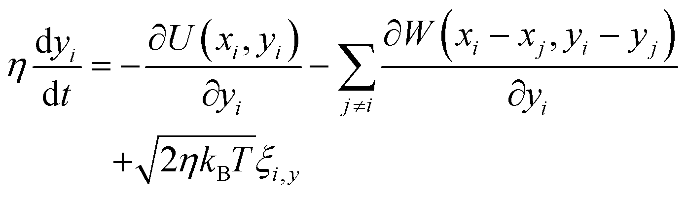
In line with the above hypothesis, the influence of radiation on filament formation effectively constrains particle drift and diffusion. Before irradiation, almost all volume between memristive terminals is available for Ag clusters, and after irradiation pinning centres for Ag clusters are created, thus forming preferable channels/valleys for Ag NPs to move between terminals. Regardless of the character of the interaction between the pinning centres and the Ag NPs, that is, whether it is attractive or repulsive, the room for particle diffusion effectively shrinks towards certain preferable paths. Such a constraint could be considered as a transition from 2D diffusion55 to the so-called “single-file diffusion”.56 The effective shrinking of the transfer space can be modelled by varying the transverse trapping potential within the commonly accepted diffusive memristor model (see the ESI in ref. 57).Within the model, two component random force (ξi,x,ξi,y) with zero mean (〈ξi,x〉,〈ξi,y〉) = (0,0) and delta-correlations in time t, 〈ξi,x(0)ξi,x(t)〉 = δ(t), 〈ξi,y(0)ξi,y(t)〉 = δ(t), and 〈ξi,x(0)ξi,y(t)〉 = 0, together with the drift force qV/L (q is the charge of the Ag cluster, V is the electric voltage, L is the gap between the electrodes or between arms of the forming filament) control diffusion of the i-th Ag NP with the coordinates (xi,yi) in a two-dimensional potential U(xi,yi) = Ux(xi) + αyi2. The potential along the x-axis Ux(xi) (see the inset in Fig. 6f) has a large minimum near one of the memristor terminals reflecting attraction to Ag-rich areas to minimize Ag–SiO interface energy, while the parabolic potential αyi2 implies constraints for transverse particle diffusion, that is, the one that is controlled by the presence of radiation-induced pinning centres, i.e. the larger α the more single-file the diffusion becomes.


 | ||
| Fig. 6 Simulated diffusion of four Ag clusters (black, red, green and blue curves) through a gap of size L located between the electrodes of a diffusive memristor which is part of an artificial spiking neuron. The diffusion is of a 2D (a, c and e) or single-file (b, d and f) character. (a and b) Spiking of conductance normalized to the maximal value; (c and d) x coordinate of a Ag cluster vs. time in the direction perpendicular to the electrodes (i.e. longitudinal diffusion); (e and f) y coordinate of a Ag cluster vs. time in the direction along the electrodes (i.e. transverse diffusion). The inset in (f) shows the potential U(x) between the terminals. | ||
Here, T is the cluster temperature, which can significantly be different from the memristor matrix temperature; T0 is the bath temperature (e.g., SiO2-matrix or memristor terminals/substrate temperature), η and kB are the Ag-cluster viscosity and the Boltzmann coefficient, while κ and C are the heat transfer coefficient and cluster heat capacity, respectively. The repulsive interaction of Ag-clusters defined by the potential W = W0 exp(−ρi,j/rint) with  prevents their agglomeration in the potential well and controls the transition from 2D to single-file diffusion.58,59 The last equation in the set is Kirchhoff's voltage law for the artificial neuron circuit with a voltage bias Vext applied to the artificial neuron, the load resistance RL, parallel capacitance CP, and RC time constant τ, that is, the model describes the spiking behaviour of our artificial neuron before and after irradiation (see Fig. 4 for the circuit scheme and experimental data). The resistance of the memristor is calculated by considering all paths between the electrodes through Ag clusters and assuming tunnelling resistance between two clusters i and j, Ri,j = exp(−ρi,j/λ) if several clusters are missed. The resistance of each path p is estimated as a series connection of tunneling resistances of all clusters in that path, and then the total memristor resistance RM is evaluated as a parallel connection of all contributing paths, such that the total conductance is:

As was shown earlier, such “compact models”51 allow us to qualitatively describe all observed experimental features and provide an insight into underlying physical phenomena. In our simulation for simplicity, we consider a case of four particles.
The dynamics of each of the four Ag particles was simulated for two cases: when lateral diffusion is high (Fig. 6a, c, and e, α = 1), representing the sample before irradiation, and when lateral diffusion is suppressed (Fig. 6b, d and f, α = 100), representing the sample after irradiation. Before irradiation, the conductance demonstrates a very complex irregular dynamics (Fig. 6a) driven by the rather erratic behavior of Ag clusters. The collective movement of different Ag particles along the x-axis (Fig. 6c, different colors) is characterized by them overtaking each other frequently which imposes randomness into the total conductance, e.g., the Ag-cluster shown by the black curve overtakes Ag clusters with other trajectories at t ≈ 0.5. This randomness is also reflected by random walks of the particles in the y-direction as illustrated in Fig. 6e. For the sample after irradiation the fluctuations in the y-direction are significantly subdued (Fig. 6f), evincing the transition from a 2D to a quasi-1D dynamics. This also makes the movement of Ag-clusters in the x-direction (see Fig. 6d) more regular, as those start to move one after another with no overtaking taking place. Such ordered collective behaviour of the Ag-clusters accelerates conductance spiking, which becomes not only more regular, but also more frequent (cf.Fig. 6a and b). Thus, these results are in perfect qualitative agreement with experimental measurements of artificial neuron spiking presented in Fig. 4b, which justifies a transition from 2D to quasi-1D drift-diffusion after irradiation as a plausible physical mechanism.
3. Conclusions
In conclusion, we experimentally and theoretically studied the effects of γ-radiation from a 60Co source on the electric properties of Ag-based diffusive memristors. The devices after irradiation demonstrated lower threshold voltages and more abrupt resistance switching between the HRS and the LRS. We also found out that artificial neurons with the memristors after irradiation demonstrated a higher frequency and more regular spiking than those with pristine memristors. These phenomena can be explained by the formation of radiation induced Si NIs which direct and accelerate the formation of CFs. Our simulations suggest that the physical mechanism of the observed dramatic change of spiking is the dynamic transition from 2D complex diffusion in the pristine samples to single-file diffusion in the samples being exposed to radiation. Our findings not only shed light on how exposure to high energy radiation affects the charge transport in diffusive memristors, but also offer an efficient way to optimise the performance of the related artificial neurons based on these memristors via the creation of artificial pinning centres. They also stimulate further research in understanding the roles of various radiation-induced defects and nano-inclusions on charge transport of memristive devices, which would promote the development of more endurable and radiation immune technological concepts.4. Methods
4.1. Sample preparation
A bottom electrode of 70 nm Pt was deposited by magnetron sputtering on a Si/SiO2 wafer, followed by co-sputtering of 60 nm of Ag and SiO2 in a mixed atmosphere of Ar and O2. A top electrode of 30 nm Pt was sputtered through a shadow mask with circular holes of 100 μm in diameter to obtain the following film structure: Si/SiO2/Pt/SiOx:Ag/Pt. All the layers were deposited at room temperature of the substrate and at a growth pressure of 5.5 mTorr. The sample preparation details were similar to the ones previously reported.16
4.2. Electrical characterization
Device contacts were made using tungsten tips housed in a probe station by Everbeing. Current–voltage characterization was performed using a Keithley 4200 SCS parameter analyzer. Unless specified otherwise the positive voltage was applied to the top electrode. For measurements of self-sustained current spikes, a voltage pulse (1 V, 50 s) was applied to the device using a Rigol waveform generator and the device voltage was recorded using a PicoScope digital oscilloscope whilst the memristor was connected in series to a load resistance RL = 65 kΩ and in parallel to a capacitor CP = 1 nF. Positive potential was applied to the top electrode and the bottom electrode was grounded.All measurements were performed under ambient conditions with no additional control over the moisture content in the atmosphere.
4.3. X-ray photoelectron spectroscopy
XPS was performed using a Thermo K-Alpha system with an Al Kα mono-chromated (1486.6 eV) source with an overall energy resolution of 350 meV. The XPS peaks are charge corrected to adventitious carbon at 284.8 eV.4.4. Radiation exposure
The gamma radiation exposure of the devices was carried out at the Dalton Cumbrian Facility using an irradiator in a self-contained Foss Therapy Services Model 812 with a 9 L sample chamber. The samples received 60Co gamma (γ) radiation with two energies of 1.17 MeV and 1.33 MeV (average energy of 1.25 MeV) at a dose rate of 229.51 Gy min−1 for exactly 217.86 minutes to give a total accumulated dose of 50 kGy. This dose was chosen as previous works on other memristive systems had reported no significant change in electrical properties at lower radiation doses.26,31 The irradiator contained three source rods with up to three source capsules (GIK-7M-4) with an initial activity of 2500 Ci per rod such that the activity was evenly distributed along the length of each source rod.Current–voltage curves were measured before and one week after exposure to radiation, except the ones for Fig. 1(e), and XPS measurements were performed one month after exposure to radiation.
4.5. Theoretical simulation
Simulation parameters are: λ/L = 0.1, rint/L = 0.04; W0/(U(−1) − U(0)) = 0.6; κτ = 90; αL2/(U(−1) − U(0)) = 1 and 100 for 2D and single-file diffusion, respectively; ; RL/min(RM) = 300; T0/(U(−1) − U(0)) = 0.0012; we use units where 2kB = 1, η = 1, and C = 1.
Conflicts of interest
There are no conflicts to declare.Acknowledgements
The authors would like to thank Sam Davis for the XPS characterization and acknowledge the use of the facilities within the Loughborough Materials Characterisation Centre. The authors acknowledge the support from the University of Manchester's Dalton Cumbrian Facility (DCF), a partner in the National Nuclear User Facility, the EPSRC UK National Ion Beam Centre and the Henry Royce Institute. We acknowledge Ruth Edge for the assistance during the gamma irradiation. This work was supported by the UK Engineering and Physical Sciences Research Council (EPSRC), grant no. EP/S032843/1.References
- D. Cooper, C. Baeumer, N. Bernier, A. Marchewka, C. La Torre, R. E. Dunin-Borkowski, S. Menzel, R. Waser and R. Dittmann, Adv. Mater., 2017, 29, 1700212 CrossRef PubMed.
- R. Waser, R. Dittmann, G. Staikov and K. Szot, Adv. Mater., 2009, 21, 2632–2663 CrossRef CAS PubMed.
- M. Lanza, H.-S. P. Wong, E. Pop, D. Ielmini, D. Strukov, B. C. Regan, L. Larcher, M. A. Villena, J. J. Yang, L. Goux, A. Belmonte, Y. Yang, F. M. Puglisi, J. Kang, B. Magyari-Köpe, E. Yalon, A. Kenyon, M. Buckwell, A. Mehonic, A. Shluger, H. Li, T.-H. Hou, B. Hudec, D. Akinwande, R. Ge, S. Ambrogio, J. B. Roldan, E. Miranda, J. Suñe, K. L. Pey, X. Wu, N. Raghavan, E. Wu, W. D. Lu, G. Navarro, W. Zhang, H. Wu, R. Li, A. Holleitner, U. Wurstbauer, M. C. Lemme, M. Liu, S. Long, Q. Liu, H. Lv, A. Padovani, P. Pavan, I. Valov, X. Jing, T. Han, K. Zhu, S. Chen, F. Hui and Y. Shi, Adv. Electron. Mater., 2019, 5, 1800143 CrossRef.
- J. J. Yang, D. B. Strukov and D. R. Stewart, Nat. Nanotechnol., 2013, 8, 13–24 CrossRef CAS PubMed.
- Z. Wang, M. Rao, R. Midya, S. Joshi, H. Jiang, P. Lin, W. Song, S. Asapu, Y. Zhuo, C. Li, H. Wu, Q. Xia and J. J. Yang, Adv. Funct. Mater., 2018, 28, 1704862 CrossRef.
- R. Wang, J.-Q. Yang, J.-Y. Mao, Z.-P. Wang, S. Wu, M. Zhou, T. Chen, Y. Zhou and S.-T. Han, Adv. Intell. Syst., 2020, 2, 2000055 CrossRef.
- Z. Wang, S. Joshi, S. E. Savel'ev, H. Jiang, R. Midya, P. Lin, M. Hu, N. Ge, J. P. Strachan, Z. Li, Q. Wu, M. Barnell, G.-L. Li, H. L. Xin, R. S. Williams, Q. Xia and J. J. Yang, Nat. Mater., 2017, 16, 101–108 CrossRef CAS PubMed.
- W. Wang, M. Wang, E. Ambrosi, A. Bricalli, M. Laudato, Z. Sun, X. Chen and D. Ielmini, Nat. Commun., 2019, 10, 81 CrossRef CAS PubMed.
- C.-P. Hsiung, H.-W. Liao, J.-Y. Gan, T.-B. Wu, J.-C. Hwang, F. Chen and M.-J. Tsai, ACS Nano, 2010, 4, 5414–5420 CrossRef CAS PubMed.
- J. V. D. Hurk, E. Linn, H. Zhang, R. Waser and I. Valov, Nanotechnology, 2014, 25, 425202 CrossRef PubMed.
- D. M. Guzman, N. Onofrio and A. Strachan, J. Appl. Phys., 2015, 117, 195702 CrossRef.
- X. Guo, C. Schindler, S. Menzel and R. Waser, Appl. Phys. Lett., 2007, 91, 133513 CrossRef.
- Z. Xu, Y. Bando, W. Wang, X. Bai and D. Golberg, ACS Nano, 2010, 4, 2515–2522 CrossRef CAS PubMed.
- Y. C. Yang, F. Pan, Q. Liu, M. Liu and F. Zeng, Nano Lett., 2009, 9, 1636–1643 CrossRef CAS PubMed.
- D.-H. Kwon, K. M. Kim, J. H. Jang, J. M. Jeon, M. H. Lee, G. H. Kim, X.-S. Li, G.-S. Park, B. Lee, S. Han, M. Kim and C. S. Hwang, Nat. Nanotechnol., 2010, 5, 148–153 CrossRef CAS PubMed.
- D. Pattnaik, Y. Ushakov, Z. Zhou, P. Borisov, M. Cropper, U. Wijayantha, A. Balanov and S. Savel'ev, Phys. Rev. Appl., 2023, 19, 024065 CrossRef CAS.
- T. R. Oldham and J. M. McGarrity, IEEE Trans. Nucl. Sci., 1983, 30, 4377–4381 Search PubMed.
- T. Oldham and F. McLean, IEEE Trans. Nucl. Sci., 2003, 50, 483–499 CAS.
- S. K. Lai, J. Appl. Phys., 1983, 54, 2540–2546 CrossRef CAS.
- C. T. Sah, IEEE Trans. Nucl. Sci., 1976, 23, 1563–1568 Search PubMed.
- A. G. Revesz, IEEE Trans. Nucl. Sci., 1977, 24, 2102–2107 Search PubMed.
- K. Yin, Y. Zhao, X. Wang, L. Liu, G. Xue, S.-T. Lee and M. Shao, Appl. Phys. Lett., 2014, 104, 033110 CrossRef.
- R. C. Hughes, Phys. Rev. Lett., 1973, 30, 1333–1336 CrossRef CAS.
- H. Hughes and J. Benedetto, IEEE Trans. Nucl. Sci., 2003, 50, 500–521 CAS.
- P. E. Dodd, M. R. Shaneyfelt, J. R. Schwank and J. A. Felix, IEEE Trans. Nucl. Sci., 2010, 57, 1747–1763 CAS.
- F. Brady, J. Maimon and M. Hurt, IEEE Trans. Nucl. Sci., 1999, 46, 1836–1840 Search PubMed.
- R. Lacoe, J. Osborn, D. Mayer, S. Brown and D. Hunt, 1998 IEEE Radiation Effects Data Workshop. NSREC 98. Workshop Record. Held in conjunction with IEEE Nuclear and Space Radiation Effects Conference (Cat. No.98TH8385), 1998, pp. 104–110.
- M. Shaneyfelt, P. Dodd, B. Draper and R. Flores, IEEE Trans. Nucl. Sci., 1998, 45, 2584–2592 CAS.
- L. J. Gerenser, J. Vac. Sci. Technol., A, 1990, 8, 3682–3691 CrossRef CAS.
- W. Chen, H. J. Barnaby, M. N. Kozicki, A. H. Edwards, Y. Gonzalez-Velo, R. Fang, K. E. Holbert, S. Yu and W. Yu, IEEE Trans. Nucl. Sci., 2015, 62, 2404–2411 CAS.
- Y. Wang, H. Lv, W. Wang, Q. Liu, S. Long, Q. Wang, Z. Huo, S. Zhang, Y. Li, Q. Zuo, W. Lian, J. Yang and M. Liu, IEEE Electron Device Lett., 2010, 31, 1470–1472 CAS.
- F. Yuan, Z. Zhang, J.-C. Wang, L. Pan, J. Xu and C.-S. Lai, Nanoscale Res. Lett., 2014, 9, 452 CrossRef PubMed.
- M. Bielmann, P. Schwaller, P. Ruffieux, O. Gröning, L. Schlapbach and P. Gröning, Phys. Rev. B: Condens. Matter Mater. Phys., 2002, 65, 235431 CrossRef.
- A. M. Ferraria, A. P. Carapeto and A. M. Botelho do Rego, Vacuum, 2012, 86, 1988–1991 CrossRef CAS.
- J. A. Rodriguez and M. Kuhn, J. Phys. Chem., 1994, 98, 11251–11255 CrossRef CAS.
- V. K. Kaushik, J. Electron Spectrosc. Relat. Phenom., 1991, 56, 273–277 CrossRef CAS.
- L. Armelao, D. Barreca, G. Bottaro, A. Gasparotto, C. Maragno and E. Tondello, Surf. Sci. Spectra, 2005, 10, 170–181 CrossRef.
- J. Wang, M. Zhou, G. Tan, S. Chen, F. Wu, J. Lu and K. Amine, Nanoscale, 2015, 7, 8023–8034 RSC.
- T. Chen, S.-Y. Liu, Q. Xie, C. Detavernier, R. L. Van Meirhaeghe and X.-P. Qu, Appl. Phys. A, 2010, 98, 357–365 CrossRef CAS.
- J. Zhao, C. Liu, J. Li, R. Wu, J. Wang, H. Qian, H. Guo, J. Li and K. Ibrahim, AIP Adv., 2019, 9, 055208 CrossRef.
- A. Mehonic, S. Cueff, M. Wojdak, S. Hudziak, O. Jambois, C. Labbé, B. Garrido, R. Rizk and A. J. Kenyon, J. Appl. Phys., 2012, 111, 074507 CrossRef.
- E. McCafferty and J. P. Wightman, Surf. Interface Anal., 1998, 26, 549–564 CrossRef CAS.
- J. A. Felix, J. R. Schwank, D. M. Fleetwood, M. R. Shaneyfelt and E. P. Gusev, Microelectron. Reliab., 2004, 44, 563–575 CrossRef CAS.
- J. R. Schwank, M. R. Shaneyfelt, D. M. Fleetwood, J. A. Felix, P. E. Dodd, P. Paillet and V. Ferlet-Cavrois, IEEE Trans. Nucl. Sci., 2008, 55, 1833–1853 CAS.
- W. Li and D. Y. Li, J. Chem. Phys., 2005, 122, 064708 CrossRef CAS PubMed.
- W. Yi, S. E. Savel'ev, G. Medeiros-Ribeiro, F. Miao, M.-X. Zhang, J. J. Yang, A. M. Bratkovsky and R. S. Williams, Nat. Commun., 2016, 7, 11142 CrossRef CAS PubMed.
- Y. Yang, P. Gao, L. Li, X. Pan, S. Tappertzhofen, S. Choi, R. Waser, I. Valov and W. D. Lu, Nat. Commun., 2014, 5, 4232 CrossRef CAS PubMed.
- A. Sarikov, V. Litovchenko, I. Lisovskyy, I. Maidanchuk and S. Zlobin, Appl. Phys. Lett., 2007, 91, 133109 CrossRef.
- M. Buckwell, L. Montesi, S. Hudziak, A. Mehonic and A. J. Kenyon, Nanoscale, 2015, 7, 18030–18035 RSC.
- F. Marchesoni and S. Savel'ev, Phys. Rev. E: Stat., Nonlinear, Soft Matter Phys., 2009, 80, 011120 CrossRef PubMed.
- W. Banerjee, S. H. Kim, S. Lee, D. Lee and H. Hwang, Adv. Electron. Mater., 2021, 7, 2100022 CrossRef CAS.
- M. Lübben, F. Cüppers, J. Mohr, M. von Witzleben, U. Breuer, R. Waser, C. Neumann and I. Valov, Sci. Adv., 2020, 6, eaaz9079 CrossRef PubMed.
- S. Tappertzhofen, I. Valov, T. Tsuruoka, T. Hasegawa, R. Waser and M. Aono, ACS Nano, 2013, 7, 6396–6402 CrossRef CAS PubMed.
- T. Tsuruoka, K. Terabe, T. Hasegawa, I. Valov, R. Waser and M. Aono, Adv. Funct. Mater., 2012, 22, 70–77 CrossRef CAS.
- U. Siems and P. Nielaba, Phys. Rev. E, 2018, 98, 032127 CrossRef CAS.
- H. Jiang, D. Belkin, S. E. Savel'ev, S. Lin, Z. Wang, Y. Li, S. Joshi, R. Midya, C. Li, M. Rao, M. Barnell, Q. Wu, J. J. Yang and Q. Xia, Nat. Commun., 2017, 8, 882 CrossRef PubMed.
- S. Savel'ev, F. Marchesoni and F. Nori, Phys. Rev. E: Stat., Nonlinear, Soft Matter Phys., 2004, 70, 061107 CrossRef PubMed.
- S. Savel'ev, F. Marchesoni and F. Nori, Phys. Rev. E: Stat., Nonlinear, Soft Matter Phys., 2005, 71, 011107 CrossRef PubMed.
- W. Sun, B. Gao, M. Chi, Q. Xia, J. J. Yang, H. Qian and H. Wu, Nat. Commun., 2019, 10, 3453 CrossRef PubMed.
| This journal is © The Royal Society of Chemistry 2023 |