
 Open Access Article
 This Open Access Article is licensed under a Creative Commons Attribution-Non Commercial 3.0 Unported Licence
Elucidating the performance benefits enabled by YSZ/Ni–YSZ bilayer thin films in a porous anode-supported cell architecture†
Katherine
Develos-Bagarinao
 *a,
Toshiaki
Yamaguchi
b and
Haruo
Kishimoto
a
*a,
Toshiaki
Yamaguchi
b and
Haruo
Kishimoto
a
aGlobal Zero Emission Research Center, National Institute of Advanced Industrial Science and Technology, AIST Tsukuba West, 16-1 Onogawa, Tsukuba, Ibaraki 305-8569, Japan. E-mail: develos-bagarinao@aist.go.jp; Tel: +81-29-861-5721
bEnergy Process Research Institute, National Institute of Advanced Industrial Science and Technology, AIST Tsukuba West, 16-1 Onogawa, Tsukuba, Ibaraki 305-8569, Japan
First published on 26th June 2023
Abstract
Increasing the performance and improving the stability of solid oxide cells are critical requirements for advancing this technology toward commercial applications. In this study, a systematic comparison of anode-supported cells utilizing thin films with those utilizing conventional screen-printed yttria-stabilized zirconia (YSZ) is performed. High-resolution secondary ion mass spectrometry (SIMS) imaging is used to visualize, for the first time, the extent of Ni diffusion into screen-printed microcrystalline YSZ electrolytes of approximately 2–3 μm thickness, due to the high temperature (typically >1300 °C) used in the conventional sintering process. As an alternative approach, dense YSZ thin films and Ni(O)–YSZ nanocomposite layers are prepared using pulsed laser deposition (PLD) at a relatively low temperature of 750 °C. YSZ thin films exhibit densely packed nanocrystalline grains and a remarkable suppression of Ni diffusion, which are further associated with some reduction in the ohmic resistance of the cell, especially in the low temperature regime. Moreover, the use of a Ni–YSZ nanocomposite layer resulted in improved contact at the YSZ/anode interface as well as a higher density of triple phase boundaries due to the nanoscale Ni and YSZ grains being homogeneously distributed throughout the structure. The cells utilizing the YSZ/Ni–YSZ bilayer thin films show excellent performance in fuel cell operation and good durability in short-term operation up to 65 hours. These results provide insights into ways to improve the electrochemical performance of SOCs by utilizing innovative thin film structures in conjunction with commercially viable porous anode-supported cells.
1. Introduction
Solid oxide cells (SOCs) can provide environmentally friendly solutions for producing continuous or on-demand power generation when operating in solid oxide fuel cell (SOFC) mode or for converting the electricity generated from renewable energy sources into fuel when operating in reverse solid oxide electrolysis cell (SOEC) mode. Due to the promising contribution of these devices to the achievement of a carbon-neutral society in the future, research in recent years has focused on addressing the important issues that must be overcome for their widespread commercialization, such as cost, efficiency, and durability.1–4 In terms of cost, a viable strategy is to innovate the materials typically used as components for the cell architecture, either through the development of novel materials or alternative processing methods.5–8 To achieve enhancements in cell performance, it is necessary to significantly reduce the contributions from the electrolyte ohmic resistance and the electrode polarization resistance. As reported in a previous study, for a typical open-circuit voltage (OCV) of 1 V, achieving a target power density of 1 W cm−2 would require a total cell area-specific resistance (ASR) of less than ∼0.25 Ω cm2. Assuming that ∼60% of this value is due to the electrolyte, the target ohmic resistance would be ∼0.15 Ω cm2.9 Achieving this target would require either a very high operating temperature or a significant reduction in electrolyte thickness. State-of-the-art yttria-stabilized zirconia (YSZ) electrolytes are typically used for SOCs, and several studies have explored the route of reducing YSZ electrolyte thickness to reduce the ohmic resistance.10,11In previous studies using micro-Raman analysis, the presence of Ni in the YSZ phase was found to be a driving force for its phase transformation from cubic to tetragonal upon reduction, accompanied by accelerated conductivity degradation.12,13 The diffusion of Ni into the YSZ electrolyte is driven by the high-temperature sintering to prepare the YSZ electrolyte on an anode support (typically a Ni-YSZ cermet). Thus, eliminating the sintering step for the YSZ electrolyte is a viable strategy to prevent or minimize the extent of Ni diffusion into the YSZ electrolyte. However, although Ni diffusion has already been identified as a key factor in the degradation of cell performance, the actual extent of Ni diffusion into the YSZ electrolyte has not been clarified using conventional analytical tools such as scanning electron microscopy or scanning transmission electron microscopy coupled with energy dispersive X-ray spectroscopy (SEM-EDX or STEM-EDX). This indicates the need for other more appropriate methods with higher sensitivity and/or resolution.
Alternative processing methods, such as pulsed laser deposition (PLD),14–16 sputtering,17–19 chemical solution deposition,20 atomic layer deposition,21–23 and ultrasonic spray pyrolysis,24,25 have been used as options for conventional screen-printing or tape-casting methods typically employed for cell fabrication. Thin film electrolytes could offer advantages over conventional electrolytes not only in terms of reliably controlled thickness reduction to the level of a few microns or less, but also in achieving densification without the sintering step typically performed at high temperatures. Thin-film electrolytes prepared using PLD and other techniques are therefore attractive alternatives to conventional sintered YSZ electrolytes. However, most studies have focused on micro-SOFCs, which have limited applications.26–28 To date, there has been no systematic investigation that clearly demonstrates the advantages of thin film electrolytes prepared using physical vapor deposition over conventional processing, especially for practical cell applications. Since most thin film processes require vacuum systems and energy sources to evaporate the materials, potentially increasing processing costs, a demonstration of superior performance is necessary to justify the economics of these techniques.
To date, only a limited number of studies have succeeded in depositing thin electrolytes on highly porous and rough substrates.29–32 However, in these studies, acceptable open circuit voltage (OCV) values of ∼1 V have only been achieved for very thin electrolyte layers in conjunction with relatively thick and dense anode functional layers,29,32 which are not ideal for gas diffusion, especially for electrolysis operation. The integration of thin-film YSZ structures into conventional SOCs based on an anode-supported cell architecture is challenging due to the highly irregular microstructures of the latter, in addition to maintaining their structural integrity during the subsequent anode reduction. For example, inadequate coverage of the Ni–YSZ anode support by the YSZ electrolyte could result in the formation of pinholes and other defects that could lead to gas leakage,11,31,33,34 or in the most extreme scenario, performance failure.
Here, we report on the development of dense thin-film bilayers consisting of Ni(O)–YSZ nanocomposite layers and thin-film YSZ electrolytes, both fabricated using PLD and without post-annealing treatment, and their successful integration into conventional anode-supported SOC cell architectures. For simplicity, the Ni(O)–YSZ nanocomposite is chosen as the material for this study in order to match that of the Ni–YSZ support and thereby eliminate the potential issues arising from the use of different materials (e.g., differences in thermal expansion coefficients, lattice mismatch, and additional cation interdiffusion). The goal of this study is twofold: first, to systematically investigate the properties of cells using thin-film YSZ electrolytes in comparison with benchmark cells using electrolyte layers by conventional screen printing and high-temperature sintering; and second, to evaluate the short-term stability and performance of cells using thin-film YSZ electrolyte layers when operated in fuel cell mode. Using advanced characterization tools including high-resolution secondary ion mass spectrometry (SIMS) imaging and transmission electron microscopy (TEM), it is shown that the use of thin films offers specific advantages such as suppression of Ni diffusion, increased density of triple phase boundaries, and maintenance of excellent contact at the YSZ and anode interfaces. In addition, the cells show excellent performance in fuel cell operation and good durability in short-term operation up to 65 hours.
2. Experimental
2.1. Cell fabrication
The NiO–YSZ anode support was prepared by extruding a mixture of 60 wt% NiO (Sumitomo Metal Mining Co., Ltd), 40 wt% YSZ (8 mol% Y2O3-doped ZrO2, Tosoh Co., Ltd) and a methylcellulose binder (Shin-Etsu Chemical Co., Ltd). The powders are then kneaded with water and extruded into a sheet about 1 mm thick. Next, an anode functional layer (AFL) was prepared by the dip-coating method, where a dip-coating slurry was prepared by ball mixing 60 wt% NiO, 40 wt% YSZ, and a polyvinyl butyral binder in a mixed solvent of ethanol and toluene for over 24 hours. The extruded sheet coated with the base layer was then cut to the desired coin size and sintered in a furnace at 1375 °C for 2 hours. Under these conditions, coin-shaped anode-supported cells with a final diameter of ∼20 mm were obtained.NiO–YSZ nanocomposite films of approximately 1 μm nominal thickness were deposited on the AFL-coated NiO–YSZ substrate using a PLD system (NanoPLD 1000/PVD Products, with a COMPexPro102 KrF excimer laser/Coherent) under the following deposition conditions: 750 °C substrate temperature, 10 mTorr oxygen partial pressure, 200 mJ laser energy, and 20 Hz laser repetition rate. The ceramic target used for the NiO–YSZ nanocomposite has a nominal composition of NiO![[thin space (1/6-em)]](https://www.rsc.org/images/entities/char_2009.gif) :YSZ = 21:79 wt%. The YSZ thin films were then deposited under the same conditions as those for the NiO–YSZ nanocomposite films.
:YSZ = 21:79 wt%. The YSZ thin films were then deposited under the same conditions as those for the NiO–YSZ nanocomposite films.
For comparison with the cells using thin films, cells using screen-printed YSZ layers (denoted as SP-1 and SP-2 in Table 1) were fabricated using the same extruded sheet dip-coated with the NiO–YSZ AFL, which was calcined at 1000 °C for 1 hour. This was then coated with a YSZ electrolyte layer using screen printing, followed by a co-sintering step at 1375 °C for 2 hours. The following identical conditions were used for the deposition of GDC interlayers on all samples: 750 °C substrate temperature, 35 mTorr oxygen partial pressure, 200 mJ laser energy, and 10 Hz laser repetition rate. A summary of the samples used in this study is shown in Table 1. For simplicity, cells using Ni(O)–YSZ nanocomposite/YSZ bilayer thin films are referred to as PLD cells, while those using screen-printed YSZ electrolytes are referred to as SP cells.
| Samples | Fabrication process | As-deposited NiO–YSZ nominal thickness (μm) | As-deposited YSZ nominal thickness (μm) | Total thickness (Ni–YSZ + YSZ) measured post-test (μm) | Post-deposition treatment |
|---|---|---|---|---|---|
| PLD-1 | PLD | ∼1.0 | ∼1.5 | 2.2 | None (as-grown) |
| PLD-2 | PLD | ∼0.7 | ∼2.6 | 3.2 | None (as-grown) |
| SP-1 | Screen-printing | — | ∼2.0 | — | 1375 °C per 2 h (YSZ) |
| SP-2 | Screen-printing | — | ∼3.0 | — | 1375 °C per 2 h (YSZ) |
After the deposition of the GDC interlayers, cathode layers consisting of LSCF–GDC (La0.6Sr0.4Co0.2Fe0.8O3−δ–Ce0.1Gd0.9O2−δ, nominal composition: 70:30 wt%) were prepared using screen printing and then sintered in air at 950 °C. The active area is fixed at 0.785 cm2. In addition, screen-printed LSC (La0.6Sr0.4CoO3−δ) layers were prepared as current collector layers on top of the LSCF–GDC cathode layers and allowed to dry (without sintering).
2.2. Electrochemical evaluation
The fabricated coin cell was characterized electrochemically using a frequency response analyzer (1260A, Solartron) with an electrochemical interface (1287, Solartron) with 3% humidified H2 gas at 100 cc min−1 and air gas at 200 cc min−1, respectively. Pt mesh and porous Ni sheet current collectors were attached to the cathode and anode, respectively, and then placed in a sample holder (CHINO Co., Ltd). Gas sealing was performed with a compression sealant under a pressure of approximately 20 N using a ceramic spring in the sample holder. The cell was heated up to 750 °C, and then the electrochemical performance was evaluated using a pseudo-four-terminal method with Pt wires.2.3. Characterization
Microstructural evaluation was performed using a field-emission scanning electron microscope (FE-SEM, Helios5 Hydra CX, ThermoFisher) operated at an acceleration voltage of 5 kV in secondary electron and backscattered electron modes for imaging. Cross-sectional observations were made on fractured samples. Average layer thicknesses were estimated from multiple measurements on cross-sectional SEM images.The elemental distribution across the cross-section of the as-prepared and post-tested samples was examined using high-resolution SIMS (NanoSIMS 50L, Ametek CAMECA) imaging analysis. Prior to the SIMS analysis, the samples were infiltrated with a high-vacuum-compatible resin, and then further fixed within the NanoSIMS specific sample holder using a Bi–Sn alloy and the surface was polished with a diamond slurry. Finally, the samples were lightly coated with evaporated osmium (Os) to improve conductivity. For SIMS measurements, a Cs+ primary ion source with a beam current of ∼23 nA and a high voltage of 8 kV was scanned over the sample surfaces. Seven secondary ion mass species of 16O−, 58Ni−, 59Co16O−, 88Sr16O−, 94Zr16O−, 140Ce16O−, and 158Gd16O− were detected simultaneously using a magnetic sector and a multi-collection system with six movable trolleys and one fixed detector. Image processing and linescan analysis were performed using WinImage ver. 4.6 software (Ametek, CAMECA).
Specimens for scanning/transmission electron microscopy (S/TEM) were prepared using dual-beam plasma focused ion beam milling (PFIB, Helios5 Hydra CX, ThermoFisher) with a Xe+ plasma source operated at 30 kV acceleration voltage for sampling and rough milling, and ~2 kV for the final thinning to achieve <100 nm thickness. S/TEM and EDX (energy dispersive X-ray spectroscopy) images were acquired using a TEM system (Tecnai Osiris, FEI) operated at 200 kV acceleration voltage.
3. Results and discussion
3.1. Microstructure
Fig. 1 shows a schematic representation of a PLD cell depicting the overall configuration of the various PLD thin films used in this study. In addition, representative plane-view SEM images depict the surface morphologies of the various PLD layers after each successive deposition. As shown in the upper left SEM backscattered electron image, the sintered AFL layer has a characteristic morphology in which the distribution of the micron-sized NiO and YSZ grains can be clearly distinguished based on the differences in contrast. Here, the dark-contrast grains are identified as those of NiO, whereas the light-contrast grains are identified as those of YSZ. The first deposited NiO–YSZ nanocomposite (PLD–NiO–YSZ, the lower left SEM image in Fig. 1) has a characteristic morphology similar to that of the underlying AFL layer, although the identification of individual NiO and YSZ grains composing the nanocomposite itself is difficult due to the limitations of SEM resolution. The second PLD layer (lower right SEM image) consisting of the YSZ thin film also shows a generally similar morphology to that of the underlying NiO–YSZ nanocomposite layer, but with very rough granular surfaces consisting of randomly oriented and faceted grains. It should be noted that the direct deposition of the YSZ thin film on the AFL/anode support resulted in a relatively different surface morphology (ESI Fig. S1†) compared to that successively grown on a NiO–YSZ nanocomposite layer. On a binary phase microstructure such as the AFL, it was found that the grains of the YSZ thin film exhibited highly different structures depending on whether they were grown on NiO or YSZ grains of the AFL. This resulted in the formation of a less homogeneous YSZ electrolyte layer with a characteristic bimodal grain distribution. The electrochemical characterization results to be discussed later will confirm that for such a cell without the NiO–YSZ nanocomposite layer, the YSZ electrolyte quality is consequently compromised. From these results, it can be concluded that the NiO–YSZ nanocomposite is critical to achieving a more homogeneous YSZ thin film. | ||
| Fig. 1 Center: schematic illustration of an anode-supported cell configuration and the representative plane-view SEM backscattered electron images of the AFL and the NiO–YSZ, YSZ, and GDC layers deposited in sequence using PLD. | ||
On the other hand, the GDC interlayer (top right SEM image in Fig. 1) exhibits a moderately different morphology due to the sharply faceted grains that characterize its surface, as well as the absence of visible grain boundaries that both the NiO–YSZ nanocomposite and YSZ thin film previously inherited from the underlying AFL. From these results, it can be further verified that all deposited PLD layers, such as the NiO–YSZ nanocomposite and YSZ and GDC thin films, appear to exhibit dense pore-free structures as well as complete coverage of the AFL/anode support.
Fig. 2 shows the representative cross-sectional SEM images of the as-prepared PLD cell (Fig. 2(a), corresponding to PLD-2 in Table 1) and the SP cell (Fig. 2(b), corresponding to SP-2 in Table 1), with the corresponding images obtained for the tested cells (Fig. 2(c) and (d)). The grain boundaries within the individual YSZ layers can be easily identified by the difference in contrast between adjacent grains. Compared to the screen-printed YSZ layers (Fig. 2(b) and (d)), whose grain sizes are in the range of a few micrometers (i.e., microcrystalline), those of the PLD–YSZ layers appear nanocolumnar with grain sizes in the sub-micrometer range (Fig. 2(a) and (c)). Nevertheless, the PLD–YSZ layer appears densely packed, and no pores or defects are visible. Below the PLD–YSZ layer, the dense Ni–YSZ nanocomposite layer can be identified by its much finer structure and mottled appearance (Fig. 2(e)). This dense Ni–YSZ nanocomposite layer is directly in contact with the Ni and YSZ grains of the underlying AFL. For the screen-printed YSZ sample, it can be observed that several areas at the YSZ interface are not in contact with the AFL (Fig. 2(d) and (f)), resulting in a limited number of triple phase boundaries (TPBs), which are considered to be active sites for electrochemical reactions.35,36 These areas are believed to have been created by the formation of pores during the reduction of NiO to Ni, or possibly Ni depletion due to migration from the interface. In contrast, the interface of the PLD-grown YSZ layer has intimate contact with the Ni–YSZ nanocomposite layer (Fig. 2(c) and (e)). The Ni–YSZ nanocomposite layer contains several nanometer-sized pores that are finely dispersed within the region. From this, it can be concluded that the Ni–YSZ nanocomposite structure consists of nanometer-sized NiO and YSZ grains that are homogeneously distributed in the initially deposited film.
 | ||
| Fig. 2 SEM backscattered electron images depicting the microstructures of the PLD cells (left column) and SP cells (right column). (a) and (b) The as-prepared cells; (c) and (d) tested cells; (e) and (f) high-magnification SEM images highlighting the YSZ/AFL interfaces of the tested PLD and SP cells, respectively. | ||
Fig. 3 shows the STEM-HAADF (high-angle annular dark field) and STEM-EDX results depicting the characteristic microstructure and elemental distribution of the PLD and SP cells after tests. In Fig. 3(a), the Ni–YSZ nanocomposite exhibits a homogeneous appearance throughout its thickness and is shown to be in intimate contact with both the YSZ thin film and the underlying porous AFL. The detailed structure of the Ni–YSZ nanocomposite is further revealed by the STEM-HAADF image shown in Fig. 3(b), with finely distributed Ni (light-contrast grains) and YSZ (gray-contrast grains) of approximately 10 nm in size, interspersed with similarly sized nanopores (dark-contrast regions). Considering that the cell has been electrochemically tested under the current load and at a high operating temperature (results will be shown later), it can be concluded that the Ni–YSZ nanocomposite exhibits structural robustness and integrity. Furthermore, there does not appear to be any pronounced clustering or formation of inhomogeneities in the distribution of the Ni and YSZ phases within the mentioned layer. It has been reported that Ni agglomeration is problematic for nanocomposites prepared using PLD,37 resulting in inhomogeneities in the distribution of Ni and YSZ phases. However, this does not seem to be an issue for the Ni–YSZ nanocomposites developed in this study because the finely formed network of the YSZ phase effectively limits the movement of Ni within the nanocomposite structure. The Ni–YSZ nanocomposite layer thus not only provides the functional support for the subsequent deposition of the YSZ thin film, but also potentially provides a high density of oxide ion pathways for a more efficient hydrogen oxidation reaction.38 On the other hand, Fig. 3(c) and (f) show the typical microstructure and elemental distribution of the SP cell, where the formation of pores due to the reduction of NiO to Ni, in addition to Ni depletion at the interface, results in less contact between the AFL and the YSZ electrolyte.
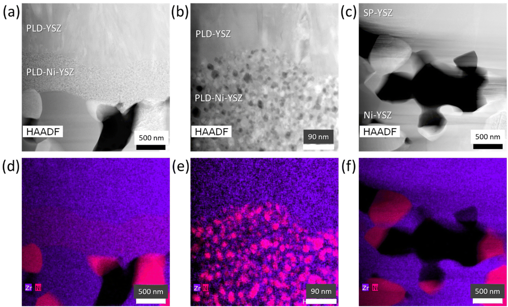 | ||
| Fig. 3 STEM-HAADF images of the tested PLD cell (a) in comparison with the SP cell (c). The corresponding STEM-EDX overlay images (Zr in purple and Ni in pink) showing the YSZ electrolyte on a Ni–YSZ nanocomposite prepared using PLD are shown below ((d) and (f)). The fine distribution of Ni and YSZ phases within the Ni–YSZ nanocomposite of the PLD cell is shown in detail in the high magnification STEM-HAADF image (b) and STEM-EDX mapping (e). | ||
Further details of the microstructure can be confirmed from the TEM image in Fig. 4(a), which shows that the highly textured YSZ thin film consists of tapered nanocolumnar grains with sizes ranging from ∼100 nm at the interface with the underlying Ni–YSZ nanocomposite and increasing to ∼200–300 nm toward the top. In contrast, as shown in Fig. 4(b), the SP–YSZ layer consists of randomly packed large grains of ∼1–2 microns in width. Therefore, the number of grain boundaries present in the YSZ thin film is estimated to be approximately 10 times lower than that in the SP–YSZ layer. In previous studies, it has been suggested that the grain boundaries could have a detrimental effect on the oxide diffusion kinetics in YSZ.39,40 It has been reported that nanostructured YSZ still exhibits a higher total conductivity compared to microcrystalline YSZ possibly due to the effect of strain40 or enhanced interfacial conductivity as reported for YSZ thin films.41 Although we believe that the presence of a relatively higher number of grain boundaries in the YSZ thin film does not necessarily indicate a disadvantage compared to the SP–YSZ layer in terms of ionic conductivity, a more systematic study is still needed to clarify the effect of grain boundaries on the performance of the YSZ layer in practical cells.
 | ||
| Fig. 4 TEM images depicting the microstructures of the (a) PLD and (b) SP cells. The PLD–YSZ thin film consists of nanocolumnar grains ∼100–200 nm in width, whereas the SP–YSZ layer consists of relatively larger micron-sized grains. | ||
3.2. SIMS imaging
To further reveal the differences between the two cell types, the high-resolution SIMS imaging technique was used to examine the distribution of Ni and Zr in the vicinity of the electrode–electrolyte interfaces. Fig. 5 shows the representative SIMS imaging results obtained for the as-prepared and tested PLD cells (Fig. 5(a)) and the as-prepared and tested SP cells (Fig. 5(b)). The mapping shows the distribution of secondary ions 58Ni and 94Zr16O−, with intensities normalized using 16O−, with the region of interest centered on the YSZ electrolyte/GDC interlayer interface. To clearly identify regions where only trace concentrations are present, the images are displayed with false color maps corresponding to intensities on a logarithmic scale (low-intensity areas depicted in blue and high-intensity areas in red). The complete SIMS data, showing other secondary ions simultaneously collected during the measurement, are shown in ESI Fig. S2 and S3.†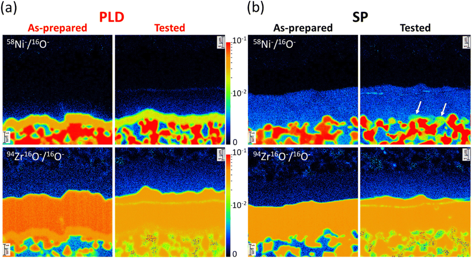 | ||
| Fig. 5 Distribution of 58Ni− and 94Zr16O− secondary ions, normalized using 16O−, across the cross-section of the (a) PLD and (b) SP cells. The left panels corresponding to each sample depict the elemental distribution of the as-prepared samples, whereas the right panels depict the corresponding distribution obtained for the tested samples. In (b), white arrows depict the locations where the Ni concentration appears to be lower (green areas). | ||
As shown in Fig. 5(a), the Ni(O)–YSZ nanocomposite layer of the PLD cell is characterized by a continuous layer of Ni which is in intimate contact with the overlying YSZ thin film as well as the Ni grains and the YSZ network of the underlying AFL structure. The contours of the thin-film bilayers essentially mimic those of the underlying AFL, which has a characteristic wavy structure. For the tested cell, the Ni distribution for the AFL appears less connected compared to the as-prepared cell due to the reduction of Ni and the formation of pores in the structure. Furthermore, the YSZ thin film does not exhibit any pronounced diffusion of Ni, unlike that of the SP cell shown in Fig. 5(b). It can be observed that Ni diffusion is already evident in the YSZ electrolyte of the as-prepared SP cell, indicating that this likely occurred during the high-temperature sintering (at 1375 °C) of the electrolyte layer. A similar distribution of Ni can be observed for the tested SP cell as well. It should be noted that the extent of Ni diffusion into the YSZ electrolyte has not yet been properly visualized in an actual cell structure; in fact, as evident in the STEM-EDX image in Fig. 3(f), no traces of Ni in the YSZ electrolyte could be detected using this analysis. Due to the high sensitivity of the SIMS analysis to detect species even at very low concentrations, this result reveals for the first time how extensive the diffusion of Ni into YSZ could be. As evidenced in Fig. 5(b), Ni has diffused through the entire thickness of the YSZ layer.
In addition, while the as-prepared SP cell has Ni regions uniformly colored in orange, the tested cell exhibits regions where the Ni concentration appears to be lower (colored in green), as indicated by the arrows in the upper right image of Fig. 5(b). These are thought to result from the volume reduction associated with the reduction of NiO to Ni and its dewetting behavior,42 which inevitably leaves regions near the YSZ interfaces with less contact with Ni. In comparison, this behavior is not obvious for the PLD cell (Fig. 5(a)), indicating that the interfacial stability at the Ni–YSZ/YSZ interfaces is maintained by the introduction of thin films.
For a semi-quantitative evaluation of the presence of Ni in the YSZ electrolyte layers, linescan profiles were extracted from the NanoSIMS mapping data as shown in Fig. 6. The NanoSIMS mapping data shown in Fig. 6(b) are composite images showing the overlay distribution of 58Ni− (shown in green), 94Zr16O− (shown in red), and 140Ce16O− (shown in blue) for the PLD and SP cells. The arrows in the images indicate the location and direction of the linescan profiles, starting from the vicinity of the YSZ layer immediately adjacent to the Ni particles and traversing its entire thickness. The small dashed rectangles indicate the width of the region of interest selected for the analysis. The 58Ni−/94Zr16O− ratio, calculated from the ratio of the respective secondary ion intensities, is extracted from the linescans and plotted as a function of distance in the corresponding graphs in Fig. 6(a).
 | ||
| Fig. 6 (a) Linescan profiles of the Ni/Zr ratio as extracted from the NanoSIMS mapping data shown on the right. (b) NanoSIMS mapping showing the composite images obtained from overlaying the secondary ions of 58Ni− (shown in green), 94Zr16O− (shown in red), and 140Ce16O− (shown in blue). Prominent peaks in the tested samples correspond to microcracks in the specimens and are considered as measurement artefacts. | ||
Focusing on the as-prepared samples, it can be easily observed that there is a strong difference in the concentration of diffused Ni for the cells. Compared to the PLD cell, the relative concentration of Ni in the YSZ electrolyte of the SP cell is higher by at least one order of magnitude throughout the entirety of its thickness. Furthermore, it can be seen that the Ni concentration is highest at the interface with the AFL, but decreases only slightly within the YSZ thickness. For the PLD cell, the Ni concentration is also relatively higher at the interface with the Ni–YSZ nanocomposite layer, but it decreases drastically along its thickness. Similarly, Ni diffusion in the YSZ electrolyte of the PLD cell is assumed to originate from the adjacent Ni–YSZ nanocomposite layer.
Next, we turn our attention to the tested samples. It can be seen that for the YSZ electrolyte of the SP cell, the amount of Ni does not change significantly compared to that before the test. This indicates that the extent of Ni diffusion is already determined at the cell preparation stage, specifically when the YSZ layer is sintered. For the PLD cell, the Ni concentration after the test became relatively higher compared to that before the test, but its profile also shows a drastic decrease along the thickness direction. This indicates that some additional diffusion of Ni from the Ni–YSZ nanocomposite layer into the YSZ thin film occurred during the test, possibly accommodated by the high-density nanocolumnar structures, although it is worth noting that the concentration of Ni in the PLD cell is still significantly lower by at least one order of magnitude compared to that of the SP cell. Prominent peaks can also be observed in the profiles of both samples; these peaks coincide with the microcracks (see the mapping data on the right) that invariably form during the specimen preparation and are therefore considered as measurement artefacts.
These results therefore provide further evidence that the thin film route is an effective approach for avoiding the excessive diffusion of Ni into the YSZ electrolyte. The main advantage is the use of a relatively low deposition temperature (750 °C) for YSZ preparation, where Ni diffusion is significantly suppressed while still obtaining a relatively dense layer capable of functioning effectively as an electrolyte for cell operation. This ensures the relative purity of the YSZ phase, thereby minimizing any conductivity degradation associated with Ni diffusion and phase transformation.12,13
3.3. Electrochemical performance
Given that the intrinsic microstructures of the YSZ layers are closely related to the fabrication process, the next question is whether these properties will have an effect on the electrochemical performance of the cells. In particular, we would like to compare the performance of the PLD cells to those with components prepared using conventional processing, in order to clarify the differences and potential advantages of using thin films in the cell architecture.Fig. 7 shows the Arrhenius-type plot of the area-specific ohmic resistance for the PLD cell (PLD-1 in Table 1), in comparison with the SP cell (SP-1 in Table 1). These results are further compared to a baseline sample that contains no thin film components, i.e., a screen-printed GDC interlayer and a YSZ electrolyte, which are typically used in conventionally prepared cells used in industry. Here we find that the ohmic resistance values for either the PLD or SP cell are at least one order of magnitude lower than those of the baseline cell. This is primarily attributed to the use of a PLD-grown GDC interlayer, which can be prepared with a dense structure at a relatively lower deposition temperature, thereby avoiding the problems of cation intermixing or solid solution formation at the interface of the GDC and YSZ electrolytes.43–45 In addition, for temperatures below 750 °C, we observed that the ohmic resistance values for the PLD cell are approximately 14–21% lower than those for the SP cell. This indicates that for an equivalent YSZ electrolyte thickness, the PLD cell outperforms the SP cell in terms of ohmic resistance. As discussed previously, this behavior can be accounted for by the relative absence of diffused Ni, as well as the intrinsically higher conductivity of nanocrystalline YSZ compared to microcrystalline YSZ. Nevertheless, we believe that even further reductions in ohmic resistance are still possible, for example, by lowering the overall electrolyte thickness, which is the subject of our ongoing investigations.
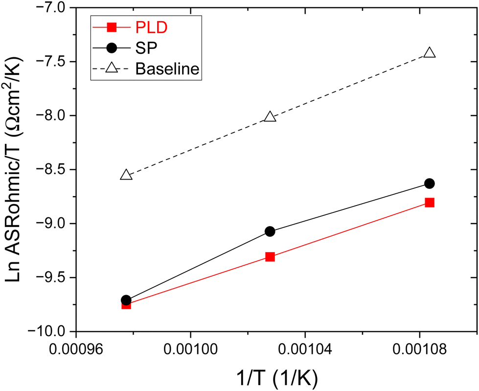 | ||
| Fig. 7 Arrhenius-type plot of the area-specific ohmic resistance comparing the performance of the PLD cell (red squares; PLD-1), the SP cell (black circles; SP-1), and a baseline sample (open triangles; no thin films included in the cell). The PLD cell shows the lowest ohmic resistance values for the entire range of temperatures investigated. | ||
Finally, Fig. 8(a) shows the current–voltage–power (I–V–P) characteristics of a PLD cell evaluated at 750 °C. The PLD cell exhibits a relatively high OCV value of ∼1.08 V, although this is still slightly below the theoretical value (1.12 V), suggesting that there is still a possibility for further optimizing the thin film structures to improve gas tightness. On the other hand, the cell prepared without a Ni-YSZ nanocomposite exhibited an even lower OCV of ~1.0 V, presumably due to insufficient gas tightness attributed to the inhomogeneous YSZ layer (ESI Fig. S1), which highlights the benefit of using the Ni-YSZ nanocomposite in the cell structure. Nevertheless, as shown in Fig. 8, a maximum power density (Pmax) of ∼1.83 W cm−2 was also obtained, which is already quite competitive with the best reported values for anode-supported cells using conventional YSZ with a similar thickness.46 As an evaluation of the short-term durability, Fig. 8(b) shows the current density at 750 °C under 3% H2O–97% H2 fuel gas flow at a constant potential of 0.8 V and plotted against the operation time. The PLD cell exhibited an initial high current density of ∼1.7 A cm−2 and showed good stability over a period of 65 hours, with only a slight reduction to ∼1.6 A cm−2. Thus, the electrochemical evaluation results confirm that the PLD cell exhibits relatively stable short-term performance. To the best of our knowledge, this is the first demonstration of stable performance using thin-film YSZ electrolytes in a conventional anode-supported cell architecture with a high current density reaching ∼1.7 A cm−2 at 0.8 V. Based on this performance, thin films therefore have great potential to replace conventionally processed components in anode-supported cells, particularly, the dense layers physically separating the porous electrodes. The majority of performance values reported in the literature, where the components of conventional materials such as YSZ and GDC were fabricated using physical vapor deposition techniques, were obtained in lower temperature regimes,30,47,48 making direct comparison with our cells difficult; not only were the temperatures much lower than those used in practical cell and stack evaluation (typically higher than 700 °C1,2,49–51), but also most studies focused only on the initial performance. A short-term evaluation by Lee et al. showed apparently stable performance at 600 °C at a constant current of only 0.2 mA cm−2 for only 7 hours;48 however, due to the relatively short period of evaluation and the absence of post-mortem analysis, it is insufficient to draw clear conclusions about the robustness and stability of the used YSZ electrolyte.
 | ||
| Fig. 8 (a) I–V–P characteristics of anode-supported PLD cell thin film layers. (b) Short-term durability of the PLD cell at a constant potential of 0.8 V at 750 °C under 3% H2O–97% H2 fuel gas flow. | ||
4. Conclusions
In this study, thin-film bilayers consisting of Ni(O)–YSZ nanocomposites and YSZ thin films have been developed for use as components in porous anode-supported cells. To understand the advantages offered by thin films, the cells were systematically compared with those obtained using conventional screen-printed YSZ. The main findings indicate that the thin film route allows the achievement of the following results:4.1. Suppression of Ni diffusion into the YSZ electrolyte
Using high-resolution SIMS imaging, extensive Ni diffusion in the conventional screen-printed YSZ electrolyte is visualized for the first time. In contrast, this behavior is strongly suppressed when using thin films. This has implications for the electrolyte-associated degradation that arises from Ni diffusion.4.2. Reduction in ohmic resistance
A lower ohmic resistance was obtained for the cells using thin films, especially in lower temperature regimes. This is attributed to the suppressed Ni diffusion as well as the nanocrystalline nature of the YSZ thin films.4.3. Increased TPBs and improved contact at the YSZ and anode interfaces
Using the Ni–YSZ nanocomposite, a fine distribution of Ni and YSZ phases at the interface was achieved, resulting in a high density of TPBs. Intimate contact is likewise maintained with both the YSZ electrolyte and the underlying AFL.To demonstrate the suitability of the developed thin-film bilayers, the electrochemical performance of the cells in fuel cell operation was evaluated. The highest maximum power density achieved was 1.83 W cm−2, and the current density at 750 °C under an applied potential of 0.8 V was as high as ∼1.75 A cm−2. Short-term durability tests performed at a constant potential of 0.8 V and 750 °C showed a high current of ∼1.7 A cm−2 and relatively stable performance up to ∼65 hours.
Thus, these results reveal that there are some specific advantages to the incorporation of thin-film layers into the architecture of commercially viable anode-supported cells, enabling good performance comparable to those utilizing components prepared using conventional methods. The demonstration of good performance using the Ni(O)–YSZ/YSZ bilayers suggests that the manufacturing approach can be a good basis for exploring other types of thin film combinations, e.g., Ni(O)–GDC, Ni(O)–scandia-stabilized zirconia, etc. The deposition parameters for the thin films should be carefully selected in order to fulfill stringent requirements such as gas-tightness, high TPB density, and the ability to maintain intimate contact with the adjacent components in the cell. On the other hand, certain issues still remain to be addressed, in terms of further improving the OCV and identifying other critical factors that may influence long-term stability. Tuning the characteristic microstructures of the thin film layers and interfacial properties is expected to further enhance performance and improve durability for long-term operation.
Author contributions
K. D.-B.: conceptualization, data curation, formal analysis, and writing – original draft, review & editing; T.Y.: conceptualization, data curation, and writing – review & editing; H. K.: conceptualization, formal analysis, and writing – review & editing.Conflicts of interest
The authors declare no competing financial interest.Acknowledgements
The authors would like to thank the technical assistance of M. Sugasawa (GZR, AIST) for the preparation of the samples, M. Sanbu for the TEM specimen preparation, and N. Saitou (TIA-EM, AIST) for the S/TEM-EDX measurements.References
- H. Yokokawa, M. Suzuki, M. Yoda, T. Suto, K. Tomida, K. Hiwatashi, M. Shimazu, A. Kawakami, H. Sumi, M. Ohmori, T. Ryu, N. Mori, M. Iha, S. Yatsuzuka, K. Yamaji, H. Kishimoto, K. Develos-Bagarinao, T. Shimonosono, K. Sasaki, S. Taniguchi, T. Kawada, M. Muramatsu, K. Terada, K. Eguchi, T. Matsui, H. Iwai, M. Kishimoto, N. Shikazono, Y. Mugikura, T. Yamamoto, M. Yoshikawa, K. Yasumoto, K. Asano, Y. Matsuzaki, K. Sato and T. Somekawa, Achievements of NEDO Durability Projects on SOFC Stacks in the Light of Physicochemical Mechanisms, Fuel Cells, 2019, 19(4), 311–339, DOI:10.1002/fuce.201800187.
- H. Yokokawa, Y. Hori, T. Shigehisa, M. Suzuki, S. Inoue, T. Suto, K. Tomida, M. Shimazu, A. Kawakami, H. Sumi, M. Ohmori, N. Mori, T. Iha, K. Yamaji, H. Kishimoto, K. Develos-Bagarinao, K. Sasaki, S. Taniguchi, T. Kawada, M. Muramatsu, K. Terada, K. Eguchi, T. Matsui, H. Iwai, M. Kishimoto, N. Shikazono, Y. Mugikura, T. Yamamoto, M. Yoshikawa, K. Yasumoto, K. Asano, Y. Matsuzaki, S. Amaha and T. Somekawa, Recent Achievements of NEDO Durability Project with an Emphasis on Correlation Between Cathode Overpotential and Ohmic Loss, Fuel Cells, 2017, 17(4), 473–497, DOI:10.1002/fuce.201600186.
- S. D. Vora, G. Jesionowski and M. C. Williams, Overview of U.S. Department of Energy Office of Fossil Energy's Solid Oxide Fuel Cell Program for FY2019, ECS Trans., 2019, 91(1), 27–39, DOI:10.1149/09101.0027ecst.
- D. Tsimis, A. Aguilo-Rullan, M. Atanasiu, E. Zafeiratou and D. Dirmiki, The Status of SOFC and SOEC R&D in the European Fuel Cell and Hydrogen Joint Undertaking Programme, ECS Trans., 2019, 91(1), 9–26, DOI:10.1149/09101.0009ecst.
- K. Develos-Bagarinao, T. Ishiyama, H. Kishimoto, H. Shimada and K. Yamaji, Nanoengineering of Cathode Layers for Solid Oxide Fuel Cells to Achieve Superior Power Densities, Nat. Commun., 2021, 12(1), 1–12, DOI:10.1038/s41467-021-24255-w.
- H. Shimada, T. Yamaguchi, T. Suzuki, H. Sumi, K. Hamamoto and Y. Fujishiro, High Power Density Cell Using Nanostructured Sr-Doped SmCoO3and Sm-Doped CeO2composite Powder Synthesized by Spray Pyrolysis, J. Power Sources, 2016, 302, 308–314, DOI:10.1016/j.jpowsour.2015.10.082.
- B. S. Kang, J. Matsuda, Y. W. Ju, H. H. Kim and T. Ishihara, Nano Strain Induced Double Columnar Oxide as Highly Active Oxygen-Dissociation Electrode for Ni-Fe Metal Supported Solid Oxide Fuel Cells, Nano Energy, 2019, 56, 382–390, DOI:10.1016/j.nanoen.2018.11.074.
- X. Tong, Y. Xu, Đ. Tripković, P. V. Hendriksen, W. R. Kiebach and M. Chen, Promotion of Oxygen Reduction and Evolution by Applying a Nanoengineered Hybrid Catalyst on Cobalt Free Electrodes for Solid Oxide Cells, J. Mater. Chem. A, 2020, 8(18), 9039–9048, 10.1039/d0ta02979c.
- E. D. Wachsman and K. T. Lee, Lowering the Temperature of Solid Oxide Fuel Cells, Science, 2011, 334(6058), 935–939, DOI:10.1126/science.1204090.
- C. J. Li, C. X. Li, Y. Z. Xing, M. Gao and G. J. Yang, Influence of YSZ Electrolyte Thickness on the Characteristics of Plasma-Sprayed Cermet Supported Tubular SOFC, Solid State Ionics, 2006, 177(19–25 SPEC. ISS.), 2065–2069, DOI:10.1016/j.ssi.2006.03.004.
- B. K. Park and S. A. Barnett, Boosting Solid Oxide Fuel Cell Performance: Via Electrolyte Thickness Reduction and Cathode Infiltration, J. Mater. Chem. A, 2020, 8(23), 11626–11631, 10.1039/d0ta04280c.
- T. Shimonosono, H. Kishimoto, M. E. Brito, K. Yamaji, T. Horita and H. Yokokawa, Phase Transformation Related Electrical Conductivity Degradation of NiO Doped YSZ, Solid State Ionics, 2012, 225, 69–72, DOI:10.1016/j.ssi.2012.05.023.
- H. Kishimoto, K. Yashiro, T. Shimonosono, M. E. Brito, K. Yamaji, T. Horita, H. Yokokawa and J. Mizusaki, In Situ Analysis on the Electrical Conductivity Degradation of NiO Doped Yttria Stabilized Zirconia Electrolyte by Micro-Raman Spectroscopy, Electrochim. Acta, 2012, 82, 263–267, DOI:10.1016/j.electacta.2012.04.148.
- A. Infortuna, A. S. Harvey and L. J. Gauckler, Microstructures of CGO and YSZ Thin Films by Pulsed Laser Deposition, Adv. Funct. Mater., 2008, 18(1), 127–135, DOI:10.1002/adfm.200700136.
- J. H. Joo and G. M. Choi, Electrical Conductivity of YSZ Film Grown by Pulsed Laser Deposition, Solid State Ionics, 2006, 177, 1053–1057, DOI:10.1016/j.ssi.2006.04.008.
- Z. Lu, J. Hardy, J. Templeton, J. Stevenson, D. Fisher, N. Wu and A. Ignatiev, Performance of Anode-Supported Solid Oxide Fuel Cell with Thin Bi-Layer Electrolyte by Pulsed Laser Deposition, J. Power Sources, 2012, 210, 292–296, DOI:10.1016/j.jpowsour.2012.03.036.
- P. Coddet, M. L. Amany, J. Vulliet, A. Caillard and A. L. Thomann, YSZ/GDC Bilayer and Gradient Barrier Layers Deposited by Reactive Magnetron Sputtering for Solid Oxide Cells, Surf. Coat. Technol., 2019, 357, 103–113, DOI:10.1016/j.surfcoat.2018.09.085.
- R. Nédélec, S. Uhlenbruck, D. Sebold, V. A. C. Haanappel, H. P. Buchkremer and D. Stöver, Dense Yttria-Stabilised Zirconia Electrolyte Layers for SOFC by Reactive Magnetron Sputtering, J. Power Sources, 2012, 205, 157–163, DOI:10.1016/j.jpowsour.2012.01.054.
- S. Sønderby, A. Aijaz, U. Helmersson, K. Sarakinos and P. Eklund, Deposition of Yttria-Stabilized Zirconia Thin Films by High Power Impulse Magnetron Sputtering and Pulsed Magnetron Sputtering, Surf. Coat. Technol., 2014, 240, 1–6, DOI:10.1016/j.surfcoat.2013.12.001.
- F. Han, R. Mücke, T. Van Gestel, A. Leonide, N. H. Menzler, H. P. Buchkremer and D. Stöver, Novel High-Performance Solid Oxide Fuel Cells with Bulk Ionic Conductance Dominated Thin-Film Electrolytes, J. Power Sources, 2012, 218, 157–162, DOI:10.1016/j.jpowsour.2012.06.087.
- S. Ji, G. Y. Cho, W. Yu, P. C. Su, M. H. Lee and S. W. Cha, Plasma-Enhanced Atomic Layer Deposition of Nanoscale Yttria-Stabilized Zirconia Electrolyte for Solid Oxide Fuel Cells with Porous Substrate, ACS Appl. Mater. Interfaces, 2015, 7(5), 2998–3002, DOI:10.1021/am508710s.
- C. C. Chao, J. S. Park, X. Tian, J. H. Shim, T. M. Gür and F. B. Prinz, Enhanced Oxygen Exchange on Surface-Engineered Yttria-Stabilized Zirconia, ACS Nano, 2013, 7(3), 2186–2191, DOI:10.1021/nn305122f.
- G. Y. Cho, Y. H. Lee, W. Yu, J. An and S. W. Cha, Optimization of Y2O3 Dopant Concentration of Yttria Stabilized Zirconia Thin Film Electrolyte Prepared by Plasma Enhanced Atomic Layer Deposition for High Performance Thin Film Solid Oxide Fuel Cells, Energy, 2019, 173, 436–442, DOI:10.1016/j.energy.2019.01.124.
- E. B. Ramirez, A. Huanosta, J. P. Sebastian, L. Huerta, A. Ortiz and J. C. Alonso, Structure, Composition and Electrical Properties of YSZ Films Deposited by Ultrasonic Spray Pyrolysis, J. Mater. Sci., 2007, 42, 901–907, DOI:10.1007/s10853-006-0004-0.
- M. F. García-sánchez, J. Peña, A. Ortiz, G. Santana, J. Fandiño, M. Bizarro, F. Cruz-Gandarilla and J. C. Alonso, Nanostructured YSZ Thin Films for Solid Oxide Fuel Cells Deposited by Ultrasonic Spray Pyrolysis, Solid State Ionics, 2008, 179, 243–249, DOI:10.1016/j.ssi.2008.01.088.
- M. Tsuchiya, B. K. Lai and S. Ramanathan, Scalable Nanostructured Membranes for Solid-Oxide Fuel Cells, Nat. Nanotechnol., 2011, 6(5), 282–286, DOI:10.1038/nnano.2011.43.
- J. L. Hertz and H. L. Tuller, Nanocomposite Platinum–Yttria Stabilized Zirconia Electrode and Implications for Micro-SOFC Operation, J. Electrochem. Soc., 2007, 154(4), B413, DOI:10.1149/1.2452902.
- A. Evans, A. Bieberle-Hütter, J. L. M. Rupp and L. J. Gauckler, Review on Microfabricated Micro-Solid Oxide Fuel Cell Membranes, J. Power Sources, 2009, 194(1), 119–129, DOI:10.1016/j.jpowsour.2009.03.048.
- H.-S. Noh, J.-W. Son, H. Lee, H.-S. Song, H.-W. Lee and J.-H. Lee, Low Temperature Performance Improvement of SOFC with Thin Film Electrolyte and Electrodes Fabricated by Pulsed Laser Deposition, J. Electrochem. Soc., 2009, 156(12), B1484, DOI:10.1149/1.3243859.
- H. S. Noh, H. Lee, B. K. Kim, H. W. Lee, J. H. Lee and J. W. Son, Microstructural Factors of Electrodes Affecting the Performance of Anode-Supported Thin Film Yttria-Stabilized Zirconia Electrolyte (∼1 Mm) Solid Oxide Fuel Cells, J. Power Sources, 2011, 196(17), 7169–7174, DOI:10.1016/j.jpowsour.2010.09.038.
- T. Van Gestel, D. Sebold and H. P. Buchkremer, Processing of 8YSZ and CGO Thin Film Electrolyte Layers for Intermediate- and Low-Temperature SOFCs, J. Eur. Ceram. Soc., 2015, 35(5), 1505–1515, DOI:10.1016/j.jeurceramsoc.2014.11.017.
- E. O. Oh, C. M. Whang, Y. R. Lee, S. Y. Park, D. H. Prasad, K. J. Yoon, J. W. Son, J. H. Lee and H. W. Lee, Extremely Thin Bilayer Electrolyte for Solid Oxide Fuel Cells (SOFCs) Fabricated by Chemical Solution Deposition (CSD), Adv. Mater., 2012, 24(25), 3373–3377, DOI:10.1002/adma.201200505.
- K. Kumada, K. Sato, T. Kawada, H. Sumi, H. Shimada and T. Hashida, Effect of Pinholes in Electrolyte on Re-Oxidation Tolerance of Anode-Supported Solid Oxide Fuel Cells, Fuel Cells, 2021, 21, 398–407, DOI:10.1002/fuce.202000062.
- C. W. Kwon, J. W. Son, J. H. Lee, H. M. Kim, H. W. Lee and K. B. Kim, High-Performance Micro-Solid Oxide Fuel Cells Fabricated on Nanoporous Anodic Aluminum Oxide Templates, Adv. Funct. Mater., 2011, 21(6), 1154–1159, DOI:10.1002/adfm.201002137.
- T. Shimura, K. Nagato and N. Shikazono, Evaluation of Electrochemical Performance of Solid-Oxide Fuel Cell Anode with Pillar-Based Electrolyte Structures, Int. J. Hydrogen Energy, 2019, 44(23), 12043–12056, DOI:10.1016/j.ijhydene.2019.03.112.
- M. Hubert, J. Laurencin, P. Cloetens, B. Morel, D. Montinaro and F. Lefebvre-Joud, Impact of Nickel Agglomeration on Solid Oxide Cell Operated in Fuel Cell and Electrolysis Modes, J. Power Sources, 2018, 397, 240–251, DOI:10.1016/j.jpowsour.2018.06.097.
- H. S. Noh, J. W. Son, H. Lee, H. I. Ji, J. H. Lee and H. W. Lee, Suppression of Ni Agglomeration in PLD Fabricated Ni-YSZ Composite for Surface Modification of SOFC Anode, J. Eur. Ceram. Soc., 2010, 30(16), 3415–3423, DOI:10.1016/j.jeurceramsoc.2010.07.035.
- K. Sato, T. Kinoshita and H. Abe, Fine-Microstructure Mediated Efficient Hydrogen Oxidation in Ni/YSZ Anode Fabricated from Novel Co-Precipitation Derived Nanocomposites, Fuel Cells, 2010, 10(2), 320–324, DOI:10.1002/fuce.200900095.
- M. Gerstl, G. Friedbacher, F. Kubel, H. Hutter and J. Fleig, The Relevance of Interfaces for Oxide Ion Transport in Yttria Stabilized Zirconia (YSZ) Thin Films, Phys. Chem. Chem. Phys., 2013, 15(4), 1097–1107, 10.1039/c2cp42347b.
- R. A. De Souza, M. J. Pietrowski, U. Anselmi-Tamburini, S. Kim, Z. A. Munir and M. Martin, Oxygen Diffusion in Nanocrystalline Yttria-Stabilized Zirconia: The Effect of Grain Boundaries, Phys. Chem. Chem. Phys., 2008, 10(15), 2067–2072, 10.1039/b719363g.
- I. Kosacki, C. M. Rouleau, P. F. Becher, J. Bentley and D. H. Lowndes, Nanoscale Effects on the Ionic Conductivity in Highly Textured YSZ Thin Films, Solid State Ionics, 2005, 176(13–14), 1319–1326, DOI:10.1016/j.ssi.2005.02.021.
- B. Song, A. Bertei, X. Wang, S. J. Cooper, E. Ruiz-Trejo, R. Chowdhury, R. Podor and N. P. Brandon, Unveiling the Mechanisms of Solid-State Dewetting in Solid Oxide Cells with Novel 2D Electrodes, J. Power Sources, 2019, 420, 124–133, DOI:10.1016/j.jpowsour.2019.02.068.
- T. Horita, N. Sakai, H. Yokokawa, M. Dokiya, T. Kawada, J. Van Herle and K. Sasaki, Ceria-Zirconia Composite Electrolyte for Solid Oxide Fuel Cells, J. Electroceram., 1997, 1(1), 155–164 CAS.
- H. Yokokawa, T. Horita, N. Sakai, K. Yamaji, M. E. Brito, Y. P. Xiong and H. Kishimoto, Ceria: Relation among Thermodynamic, Electronic Hole and Proton Properties, Solid State Ionics, 2006, 177(19–25 SPEC. ISS.), 1705–1714, DOI:10.1016/j.ssi.2006.03.006.
- X. D. Zhou, B. Scarfino and H. U. Anderson, Electrical Conductivity and Stability of Gd-Doped Ceria/Y-Doped Zirconia Ceramics and Thin Films, Solid State Ionics, 2004, 175(1–4), 19–22, DOI:10.1016/j.ssi.2004.09.040.
- B. K. Park and S. A. Barnett, Boosting Solid Oxide Fuel Cell Performance: Via Electrolyte Thickness Reduction and Cathode Infiltration, J. Mater. Chem. A, 2020, 8(23), 11626–11631, 10.1039/d0ta04280c.
- J. H. Park, S. M. Han, K. J. Yoon, H. Kim, J. Hong, B. K. Kim, J. H. Lee and J. W. Son, Impact of Nanostructured Anode on Low-Temperature Performance of Thin-Film-Based Anode-Supported Solid Oxide Fuel Cells, J. Power Sources, 2016, 315, 324–330, DOI:10.1016/j.jpowsour.2016.03.055.
- Y. H. Lee, H. Ren, E. A. Wu, E. E. Fullerton, Y. S. Meng and N. Q. Minh, All-Sputtered, Superior Power Density Thin-Film Solid Oxide Fuel Cells with a Novel Nanofibrous Ceramic Cathode, Nano Lett., 2020, 20(5), 2943–2949, DOI:10.1021/acs.nanolett.9b02344.
- T. Horita, H. Kishimoto, K. Yamaji, M. E. Brito, Y. Xiong, H. Yokokawa, Y. Hori and I. Miyachi, Effects of Impurities on the Degradation and Long-Term Stability for Solid Oxide Fuel Cells, J. Power Sources, 2009, 193(1), 194–198, DOI:10.1016/j.jpowsour.2008.10.127.
- Q. Fang, C. E. Frey, N. H. Menzler and L. Blum, Electrochemical Performance and Preliminary Post-Mortem Analysis of a Solid Oxide Cell Stack with 20,000 h of Operation, J. Electrochem. Soc., 2018, 165(2), F38–F45, DOI:10.1149/2.0541802jes.
- F. Monaco, D. Ferreira-Sanchez, M. Hubert, B. Morel, D. Montinaro, D. Grolimund and J. Laurencin, Oxygen Electrode Degradation in Solid Oxide Cells Operating in Electrolysis and Fuel Cell Modes: LSCF Destabilization and Interdiffusion at the Electrode/Electrolyte Interface, Int. J. Hydrogen Energy, 2021, 46(62), 31533–31549, DOI:10.1016/j.ijhydene.2021.07.054.
Footnote |
| † Electronic supplementary information (ESI) available. See DOI: https://doi.org/10.1039/d3nr01604h |
| This journal is © The Royal Society of Chemistry 2023 |