Preferential perovskite surface-termination induced high piezoresponse in lead-free in situ fabricated Cs3Bi2Br9-PVDF nanocomposites promotes biomechanical energy harvesting

Aditi Sahoo a, Tufan Paul a, Ankan Nath b, Soumen Maiti c, Prabhat Kumar a, Prasenjit Ghosh b and Rupak Banerjee *ad
aDepartment of Physics, Indian Institute of Technology Gandhinagar, Palaj, Gandhinagar 382355, India. E-mail: rupakb@iitgn.ac.in
bDepartment of Physics, Indian Institute of Science Education and Research, Dr. Homi Bhabha Road, Pune 411008, India
cSt. Thomas Colleges of Engineering & Technology, Kolkata 700023, India
dK C Patel Centre for Sustainable Development, Indian Institute of Technology Gandhinagar, Palaj, Gandhinagar 382355, India

Received 1st April 2023 , Accepted 19th June 2023

First published on 20th June 2023


Abstract

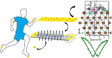
Lead-free halide perovskites have gained immense popularity in photovoltaic and energy harvesting applications because of their excellent optical and electrical attributes with minimal toxicity. We synthesized composite films of lead-free Cs3Bi2Br9 perovskite embedded in the polyvinylidene fluoride (PVDF) matrix and have investigated their piezoelectric energy harvesting. Five PVDF@Cs3Bi2Br9 composite films were fabricated with varying wt% of the perovskite in the PVDF. The composite with a 4 wt% of the perovskite shows 85% activation of the electroactive β-phase of PVDF. Additionally, this composite exhibits a maximum polarisation of ∼0.1 μC cm−2 and the best energy storage density of ∼0.8 mJ cm−3 at an applied field of ∼16 kV cm−1 among all the synthesized composites. A nanogenerator fabricated using 4 wt% loading in the composite film produced an instantaneous output voltage of ∼40 V, an instantaneous current of ∼4.1 μA, and a power density of ∼17.8 μW cm−2 across 10 MΩ resistance when repeatedly hammered by the human hand. The nanogenerator is further employed to light up several LEDs and to charge capacitors with a small active area demonstrating significant promise for prospective wearables and portable devices and paving the way for high-performance nanogenerators using lead-free halide perovskites. Density functional theory calculations were performed to understand the interaction of the electroactive phase of the PVDF with different perovskite surface terminations to unravel the various interaction mechanisms and their ensuing charge transfer properties.


1. Introduction

The accelerated depletion of fossil fuels and the unprecedented climate changes induced by harnessing energy from them has necessitated intense research efforts in renewable energy sources and technologies, particularly those which are environment-friendly with a low carbon footprint. In addition to renewable energy sources, the realization of low-power electronic devices is also the present need of the hour.1–6 Different types of energy sources like electrostatic, thermal, solar, vibration, wind, and sonic waves are present in our circumambient and are used to produce wearable devices.7–9 In this context, piezoelectric nanogenerators (PENGs) are playing an important role due to their ability to harvest “battery-less” energy from ambient sources.10,11 Considerable efforts have been devoted to exploring potential materials and structures that can be employed to build PENGs with high electrical output. Given its electroactive phase content and excellent flexibility, polyvinylidene fluoride (PVDF) and its copolymers are among the most attractive choices.12,13 However, bare PVDF-based nanogenerators have limited electrical output and cannot meet the increased energy demands. One of the many successful ways to increase PVDF's electrical output is to alter its physical and chemical properties by adding functional fillers.14,15 In addition to their deployment in optoelectronic devices like solar cells, LEDs, and photodetectors, halide perovskites (compared to other additive materials) offer attractive possibilities as a filler to increase the performance of a PENG.16–21 This is primarily because halide perovskites can act as potent nucleating agents for PVDF due to their semiconducting and ionic properties, resulting in the transformation of amorphous or nonpolar phases into polar-crystalline phases with improved piezoelectric responses.22,23

Despite these apparent advantages, most research so far has focused on lead-based halide perovskites,24–29 which are detrimental to both human and environmental health due to toxic lead components. At the same time, some lead-free tin-based perovskites, despite their low toxicity, have shown instability and oxidation issues.30 All-inorganic bismuth-based halide perovskite materials, with a typical formula of A3Bi2X9 (A: Cs, X: I, Br, Cl), have drawn significant attention in the development of improved lead-free perovskite materials due to their superior power conversion efficiency, structural stability, and low toxicity.31,32 Recently, Cs3Bi2Cl9, a bismuth-based perovskite, has been reported in photodetection and CO2 reduction applications.33–35 In bismuth-based perovskites, Bi3+ has the advantage of having not only an electronic configuration similar to Pb2+ but also a comparable ionic radius, and, in fact, Cs3Bi2Br9 perovskite-derivates demonstrated high photoluminescence quantum yields as well as moisture and air stability.36 Extensive research is being done to enhance the Cs3Bi2Br9-based device's water retardancy, functionality, and encapsulation in order to increase its working lifespan. Mechanical energy harvesting or self-powered electronics is desirable in this scenario, but the brittle nature of halide perovskite, which might easily lead to material breakage during mechanical deformations of wearable devices, presents yet another obstacle to its practical application. Perovskites demonstrate exceptional mechanical durability and flexibility when combined with flexible PVDF polymer to create a homogeneous composite. The PVDF-halide perovskite composite also offers an additional protective layer to prevent direct contact between perovskites and the external atmosphere, thereby significantly improving its mechanical properties and overall stability.37 In general, the PVDF polymer exhibits four distinct polymorphs: the α, β, γ, and δ phases. Due to their dominant piezoelectric and ferroelectric properties, the semi-polar γ (T3GT3G conformation) and the polar β (TTTT conformation) phases are particularly significant for energy harvesting.38 Compared to other phases, the β-phase has a larger dipole moment per unit volume (enhanced electroactivity) because its dipole moment is aligned perpendicular to the central chain axis of the PVDF.39,40 Most previously documented approaches for making perovskite-PVDF composites are impeded by the physical mixing approach, which frequently results in aggregation in the polymer matrix leading to reduced interfacial interaction between the constituents.41In situ strategies, on the other hand, provide good dispersion and distribution of the constituent elements in the composite. Direct integration of a well-dispersed nanostructure into a polymer matrix is also possible using these approaches.42 Furthermore, the majority of studies on perovskite-based composites have focused on photovoltaic applications, while only a small fraction has investigated mechanical energy harvesting, leaving ample scope for advancement in this area of potentially affordable technology.43–45

In this study, we used an in situ chemical method to create a composite film using PVDF and Cs3Bi2Br9 nanostructures at ambient temperatures. The key features of this technique are the relatively uncomplicated synthesis strategies along with a high yield. The PVDF@Cs3Bi2Br9 composite is made in situ, ensuring that the perovskite is evenly distributed throughout the PVDF polymer matrix. When used as a filler, the Cs3Bi2Br9 perovskite facilitates substantial electroactive β-phase transformation in the polymer matrix. Several weight percentages of the perovskite were combined with the PVDF to fabricate the optimized composite for energy harvesting applications. Diffraction and spectroscopic studies were carried out to assess the electroactive phase change with increasing perovskite content in the composite. The electroactive phase in the PVDF matrix could be enhanced beyond 85% in the optimized PVDF@Cs3Bi2Br9 composite, which also exhibited butterfly-shaped amplitude and phase loops. The device fabricated from this optimized film demonstrated the highest energy harvesting capability among all the synthesized samples due to its superior piezoelectric properties. The piezoelectric performance of the optimized composite is significantly better than that of pristine PVDF. The enhanced piezoresponse in the composites is explained in terms of the interaction between the polymer and the perovskite surface terminations. The interfacial interactions of PVDF molecules with Cs3Bi2Br9 perovskite were demonstrated using the first principles density functional theory (DFT) based calculations. The proposed approach illustrates the potential of employing lead-free perovskite-PVDF composites to obtain substantially increased piezoresponse for high-performance energy harvesting devices based on biomechanical motions.

2. Experimental

2.1 Chemicals and materials

Cesium bromide (CsBr), bismuth bromide (BiBr3), PVDF pellets (Mw 275[thin space (1/6-em)]000 g mol−1), Isopropyl alcohol (IPA), and Al tape strip were procured from Sigma Aldrich, USA. On the other hand, N,N-dimethyl formamide (DMF), Polydimethylsiloxane (PDMS), and Acetone were obtained from Merck, India.

2.2 Cs3Bi2Br9 synthesis

0.2 mmol bismuth(III) bromide (BiBr3) and 0.3 mmol Cesium bromide (CsBr) were mixed in 2 ml of DMF and stirred for 45 minutes separately at room temperature. After that, both solutions were added and left at room temperature for 12 hours under continuous stirring. The final solution was then precipitated with 20 ml of IPA and centrifuged at 5000 rpm, after which the precipitate was left for 12 hours to dry in vacuum.

2.3 In situ synthesis of Cs3Bi2Br9 in PVDF matrix

By mixing 0.3 mmol CsBr and 0.2 mmol BiBr3 into a 15 ml DMF and PVDF solution, the in situ synthesis of Cs3Bi2Br9 on the PVDF matrix was realized. This mixture solution was stirred for 12 hours at 60 °C. The resulting mixed solution was then put onto a glass surface and Petri dish to create a uniformly thick coating. The glass substrate and Petri dish are then placed in a vacuum oven set to 90 °C for 24 hours. Finally, a clean tweezer was used to peel the in situ perovskite PVDF composite films (IPPF) away from the substrate. Five in situ composite films are coined as IPPF2, IPPF3, IPPF4, IPPF5, and IPPF6, where the numeric suffix represents the wt% of the perovskite in the composite. All the cast films were further used for detailed characterizations and device applications. For device fabrication, we used 5 × 2 cm2 effective area of the composite films. We applied aluminium foil tapes on both sides of the nanocomposite films with an area of 4.8 × 1.8 cm2. Between the nanocomposite and the aluminium foil strip, copper wires were connected. Furthermore, the device was encapsulated with PDMS and then heated in an electric furnace at 70 °C until the PDMS hardened. The in situ nanogenerator (ING) device required the PDMS encapsulation to prevent damage from repetitive mechanical excitations and to make it water and dust resistant.16Fig. 1 shows the schematic representation of the in situ synthesis procedure.
image file: d3nr01517c-f1.tif
Fig. 1 Schematic representation of in situ fabrication of PVDF@Cs3Bi2Br9 composite-based PENGs.

3. Characterization

X-ray diffraction (XRD) measurement was performed at room temperature using Cu-Kα radiation (λ = 1.5406 Å) on a SmartLab Multipurpose X-ray diffractometer (Rigaku Corp., Japan). The UV-Vis absorbance spectrum was studied using a UV-Vis NIR Carry 5000 Agilent spectrometer. NEXA base Thermo Fischer Scientific X-ray photoelectron spectroscopy (XPS) was used to determine the elemental composition and the oxidation states of the prepared material. Field Emission Scanning Electron Microscopy (FESEM) and Energy Dispersive X-ray (EDX) spectroscopy were performed using Supra 35 VP for microstructural and elemental analysis, respectively. Fourier Transform Infrared Spectroscopy (FTIR) (FTIR-Spectrum 2, PerkinElmer) was used to determine the phase parameters of the samples. The piezoresponse force microscopy (PFM) study was performed on an Asylum Research AFM (MFP-3D BIO). Dielectric measurements were made using an LCR spectrometer (HIOKI, model: IM 3536). The RADIANT ferroelectric test apparatus (Radiant Technologies Inc.) and Vision software were used to perform the room-temperature ferroelectric measurement. A digital oscilloscope (YOKOGAWA, DL 1640) was used to record the piezoresponse.

4. Computational details

We have carried out DFT-based studies using the Quantum Espresso software.46,47 The electron-ion interactions are described with ultrasoft pseudopotentials48 for Bi, Br, C, and F, while for Cs, we have used a norm-conserving pseudopotential.49 The following valence electron configurations were considered for the different species: Cs: 6s1, Bi: 5d106s26p3, Br: 4s24p5, C: 2s22p2, F: 2s22p5 and H: 1s1. The electron–electron exchange and correlation potentials were treated within the generalized gradient approximation (GGA) using the Perdew–Burke–Ernzerhof (PBE) parametrization.50 The wavefunctions and charge densities are expanded using a plane wave basis set with a kinetic energy cutoff of 55 Ry (550 Ry) for the wavefunction (charge density). The Br ions being highly polarizable, van der Waals interactions are important for these systems. Moreover, as shown later, van der Waals interactions are also crucial for describing the PVDF-Cs3Bi2Br9 interface. Since conventional DFT functionals do not include van der Waals interaction, we have incorporated this using the semi-empirical Grimme's DFT-D2 correction.51 Brillouin zone (BZ) integrations were done using Γ-centered Monkhorst–Pack k-point mesh of (5 × 5 × 3) for bulk Cs3Bi2Br9 and shifted k-point meshes of (10 × 3 × 6) for the β phase of PVDF, respectively. To speed up the calculations, we have used a Marzari-Vanderbilt smearing52 with a smearing width of 0.007 Ry.

In order to test the validity of our computational parameters, we have computed the lattice parameters of bulk Cs3Bi2Br9 and the β phase of PVDF. Bulk Cs3Bi2Br9 crystallizes in the trigonal P3m1 space group. Our computed lattice parameters of a = 7.72 Å and c = 9.53 Å are in excellent agreement with the experimental values of 7.90 Å and 9.85 Å.53 For the β phase of PVDF, our calculations yield lattice parameters of a = 2.57 Å, b = 8.26 Å, and c = 4.55 Å that are in reasonably good agreement with the literature report.54

In order to study the interaction between the polymer and the halide perovskite, we have considered the (0001) surface of the latter. Cleaving the crystal along the [001] direction can result in two possible terminations, namely, the CsBr3 and the Bi terminations (Fig. 2). While, in the former, the surface layer of the (1 × 1) surface unit cell has one Cs and three Br, for the latter, the Bi atoms form the surface layer. As a consequence, some of the Cs and Br atoms of the layer below the Bi layer are also exposed in the Bi termination. Each of these terminations were modeled by symmetric slabs. For the CsBr3 (Bi) termination, the slab consists of 6 alternating CsBr3 and Bi layers (9 layers). Since we are using periodic boundary conditions, we have used a vacuum of 25 Å along the direction perpendicular to the slab to minimize the spurious interactions between the periodic images. Moreover, for the (1 × 1) surface unit cell, we have used a (5 × 5 × 1) k-mesh. A single strand consisting of 3 monomeric units of β-PVDF was placed on a (2 × 1) surface supercell at different places to study the interaction of β-PVDF with Cs3Bi2Br9. A single strand of the polymer, with one monomer unit in the unit cell, has a periodicity of 2.58 Å. Thus 3 monomeric units were placed along the shorter axis of the surface supercell, resulting in a minimal compressive strain of −0.26% on the PVDF strand.


image file: d3nr01517c-f2.tif
Fig. 2 Bulk structure of Cs3Bi2Br9 showing the stacking of the atoms along the [001] direction. The red box shows the bulk unit cell in the ac plane. The black boxes show the CsBr3 and Bi layers.

5. Results and discussion

XRD and FTIR spectroscopy were performed for the characterization of the structural phases and quantification of electroactive β-phase in the in situ grown composite films. Fig. 3(a) shows XRD measurements of pure Cs3Bi2Br9, pure PVDF, and the composite films with varying Cs3Bi2Br9 percentage loading. Diffraction peaks corresponding to the PVDF and Cs3Bi2Br9 are present in all the composite films (IPPF2, IPPF3, IPPF4, IPPF5, IPPF6). With the increment in the Cs3Bi2Br9 loading into the PVDF matrix, the diffraction peaks of Cs3Bi2Br9 become more pronounced. The characteristic diffraction peaks of the Cs3Bi2Br9 nanostructures at 2θ of 15.72° (100), 18.02° (002), 22.28° (102), 27.2° (003), 31.7° (202), and 39.07° (212) indicate the formation of pure Cs3Bi2Br9 perovskite with a hexagonal crystal structure in the PVDF matrix. Fig. S1(a) in the ESI shows the deconvoluted XRD peaks of PVDF, which represent the α-, β-, and γ-phases in the bare film. The characteristic peaks at 19.1° (020) and 20.2° (200) confirm the presence of nonpolar α-phase and semi-polar γ-phase in pure PVDF, respectively. Deconvoluted XRD peaks of the composite films IPPF2, IPPF3, IPPF4, IPPF5, and IPPF6 are shown in Fig. S1(b), (c), (d), (e), and (f) (please see ESI), respectively. From the variation in the relative intensities of the peaks corresponding to the α- and the β-phases, it can be concluded that the electroactive β-phase increases with an increase in the perovskite loading into the PVDF at the expense of the α-phase. The maximum amount of activated β-phase was found for the IPPF4 sample. Beyond this, the amount of polar phase shrinks as the perovskite loading increases. Fig. 3(b) shows the FTIR measurements confirming the nucleation of the electroactive β-phase in the Cs3Bi2Br9@PVDF composite films. The FTIR spectrum of pure PVDF reveals typical absorption peaks at 432 cm−1, 764 cm−1, 812 cm−1, 1150 cm−1, and 1233 cm−1, demonstrating the presence of nonpolar and semi-polar phases. The intensity of distinct absorption peaks corresponding to the nonpolar α-phase is rapidly diminished with the addition of Cs3Bi2Br9 to the PVDF matrix. On the other hand, the intensity of absorption peaks related to the polar β-phase continuously rises with the loading of perovskite in the PVDF matrix. The appearance of sharp peaks at 468 cm−1, 840 cm−1, and 1279 cm−1 demonstrates the formation of the polar β-phase in the composite film. Fig. 3(c) shows the variation in the electroactive phase percentage (FEA) as a function of perovskite loading.
image file: d3nr01517c-f3.tif
Fig. 3 (a) XRD profile, (b) FTIR spectra, and (c) the electroactive β-phase percentage of the pure PVDF and the composite samples.

The following formula is used to quantitatively analyze the electroactive phase composition in the perovskite-PVDF composite matrix:

image file: d3nr01517c-t1.tif
where FEA is the electroactive phase fraction. A764 and A840 are the absorption peak intensities at 764 cm−1 (non-electroactive phase) and 840 cm−1 (electroactive phase), respectively. K764 and K840 are the absorption coefficients corresponding to the peaks at 764 cm−1 and 840 cm−1, respectively, with values of 6.1 × 104 cm2 mol−1 and 7.7 × 104 cm2 mol−1. With 4 wt% Cs3Bi2Br9 loading, the phase percentage reached >85%, more than thrice as high as the pristine PVDF phase percentage (25%). When the perovskite loading was increased by more than 4 wt%, the nonpolar α-phase increased, possibly due to perovskite aggregation in the PVDF matrix at higher loading.14 The FTIR spectrum in the range of 3050–2960 cm−1 in Fig. S2 (please see ESI) clearly shows the interfacial interaction between Cs3Bi2Br9 and the PVDF dipoles. The symmetric and asymmetric –CH2– bond stretching absorption peaks at 2980 and 3023 cm−1 are crucial in understanding the generation of electroactive phases via interfacial contact.14 The shift in the vibrational peaks is indicative of interfacial interaction. Both peaks are blue-shifted when comparing PVDF solely to composite films, indicating an interaction between the perovskite and PVDF dipole. The surface charge of Cs3Bi2Br9 interacts interfacially with –CH2– and –CF2– dipoles. This interaction promotes the preferred ordering of PVDF chains from α (TGTG) to β (TTTT) phase, resulting in an increase in the percentage of electroactive β-phase in the PVDF matrix.14 The –CH2– dipole's effective mass rises due to the interfacial interaction, which lowers its vibrational frequency. As a result, this interaction serves as a damping source. The angular frequency of the –CH2– stretching vibration dipole under damped and undamped conditions is correlated with the damping constant. The amount of perovskite in the composite film raises the value of the damping constants. It is worth noting that under perovskite loading, the behavior of the electroactive β-phase and the damping constant is similar, which indicates a direct link between electroactive phase growth in the PVDF matrix as a result of dipolar interaction with Cs3Bi2Br9.38 The amount of electroactive PVDF phase and the crystalline structure of the PVDF present in a PVDF-based composite film govern the system's piezoelectric capabilities.

The X-ray photoelectron spectroscopy (XPS) surface survey scan of the IPPF4 film is depicted in Fig. 4(a). XPS analysis validates the existence of Cs, Bi, Br, C, and F as the constituent elements as well as their chemical states. All the spectra were charge corrected by referencing the C 1s peak positioned at 284.75 eV. The prominent peaks at 723.23 and 737.19 eV in Fig. 4(b) correspond to Cs 3d5/2 and Cs 3d3/2, respectively. This indicates that the CsBr primordial reactant is not present in the PVDF@Cs3Bi2Br9 composite fibers as-synthesized but is instead introduced to the perovskite structure as a monovalent ion.55 The Bi3+ state is represented by two peaks in Fig. 4(c) that are indexed to the Bi 4f7/2 and Bi 4f5/2 core levels, respectively, with energies of 158.17 eV and 163.53 eV.56 The two Br 3d peaks, ascribed to the 3d3/2 and 3d5/2 states, are visible in the Br 3d spectrum (see Fig. 4(d)). In the composite film, the Br 3d3/2 and 3d5/2 peaks are found at 66.97 eV and 67.85 eV, respectively.57 The C 1s spectrum is deconvoluted into three peaks at 284.17, 286.03, and 289.36 eV, as shown in Fig. 4(e). The CH2 bond is responsible for the first two peaks, whereas the CF2 bond is associated with the third peak. Fig. 4(f) illustrates the F 1s peak, which is symmetric at 686.61 eV. For the composite IPPF4, C 1s and F 1s peaks are found to be shifted towards higher binding energies, whereas the Cs 3d, Bi 4f, and Br 3d peaks are shifted towards lower binding energies with respect to the pristine PVDF and Cs3Bi2Br9 samples.58 Such a shift in binding energies may be attributed to the production of an internal electric field due to hybrid formation, which substantially impacts the local binding energies of the base materials.15Fig. 4(g) displays a representative FESEM image of the in situ synthesized IPPF4 composite film demonstrating the presence of nearly uniform connected spherical structures. Fig. 4(h) shows the EDX spectra, and Fig. 4(i) the EDX elemental mapping of the IPPF4 sample, affirming that the composite film is indeed comprised of C, F, Cs, Bi, and Br and is homogenously distributed with almost no impurities. Fig. S3 and S4 (please see ESI) display the FESEM images and the EDX mapping of the other composites.


image file: d3nr01517c-f4.tif
Fig. 4 (a) XPS surface survey; core level, (b) Cs 3d, (c) Bi 4f, (d) Br 3d (e) C 1s, (f) F 1s spectra, (g) FESEM, (h) EDX spectra, and (i) EDX elemental mapping of the IPPF4 film.

The magnitude of the material's piezoelectric coefficient (d33) represents the ability of a piezoelectric material to transform mechanical stress into electricity. The piezoelectric coefficient of a material significantly influences its piezoresponse. In order to assess the piezoelectric features of the composite with a 4 wt% perovskite loading, we used piezoresponse force microscopy (PFM). The conductive tip served as one of the electrodes during this PFM, with the applied electrical field running parallel to the detected deformation. Fig. 5(a), (b), and (c), respectively, show the obtained amplitude, phase, and topography images in an area of 5 μm × 5 μm. With a bias voltage of ±30 V, a butterfly-shaped amplitude loop [A(E)] was seen in Fig. 5(d). The amplitude of this composite film (IPPF4) reaches 425 pm (OFF state) over the ±30 V voltage range without poling. The formula for determining the piezoelectric coefficient is Adeflection = d33Eac. From this equation, the d33 value for IPPF4 was calculated to be 10 pm V−1. This value exceeds that of other lead-free perovskites, such as NaNbO3 (4 pm V−1),59 and lead-based organic halide perovskites, such as MAPbI3 (5 pm V−1).60 Table S1 (please see ESI) shows the piezoelectric coefficient (d33) values of different piezoelectric materials for comparison.


image file: d3nr01517c-f5.tif
Fig. 5 PFM response: (a) amplitude (b) phase image (c) topography (d) “butterfly” loop (e) phase hysteresis loop and (f) piezoresponse loop obtained with a DC voltage of ±30 V.

Fig. 5(e) shows the phase response of IPPF4 when the bias voltage is applied. Applying an external electric field makes it possible to change the polarization upward or downward, as shown by the rectangle-shaped hysteresis loop of IPPF4 composite film, demonstrating 180° switching. The “OFF” state is utilized for these experiments to reduce the impact of electrostatic interactions. Fig. 5(f) depicts the calculated piezoresponse hysteresis loop using the equation: PR(E) = A(E) cos[φ(E)].61,62 The resultant hysteresis loop is asymmetric, indicating a transition toward positive bias along the electric field axis, which further suggests that the nanocomposite already has a built-in field that encourages polarization in a particular direction.63

Particularly in the context of designing energy storage devices, the dielectric features of composite films are significant. The dielectric constant value can estimate a material's charge-carrying capacity, and the dielectric loss (tan[thin space (1/6-em)]δ) measures the energy dissipation (power loss) in each cycle. The relative dielectric permittivity (εr) of bare PVDF and the composite films at ambient temperature in the frequency range of 50 Hz to 1 MHz is shown in Fig. 6(a), where we observe that the εr values of the composite films are higher than the pristine PVDF. Here, the permittivity value rises as the amount of perovskite is increased, which may result from increased interfacial interaction between the perovskite and PVDF matrix. Furthermore, it is observed that in all the composite films, the value of εr for IPPF4 is maximum and that a perovskite loading of more than 4 wt% actually reduces the relative permittivity due to agglomeration.64 In composite materials, the higher dielectric constant can be explained by the Maxwell–Wagner polarization. The PVDF matrix acts as an insulating layer between the Cs3Bi2Br9 perovskite structures, which results in a capacitor-like arrangement within the matrix. This is very similar to the behavior of semiconductor nanoparticles inside the polymer matrix, which work like micro-capacitors leading to enhancement in the dielectric constant and, consequently, the energy density of the polymer-dielectric composites.65–67 Appreciable amount of charges is held in PVDF@Cs3Bi2Br9 composite micro capacitors due to the insulating layer's attempt to stop the generation of high leakage currents.68 The consequence is an increase in dielectric permittivity.15 On the other hand, incorporating perovskite into a hybrid raises the interfacial space charge, resulting in increased space charge polarisation and a rise in the dielectric permittivity (εr) value.15 These two aspects influence the relative dielectric permittivity of the composite. As mentioned earlier, if the perovskite value is increased by more than 4 wt%, the composite system agglomerates, which can cause the insulating layer between the two perovskite structures to disappear, resulting in the decrement of the capacitance value. A drop in εr values for the hybrid composites is registered at high frequencies. The relatively larger values of εr at low frequencies can be explained by the existence of all four types of polarizations, including ionic, electronic, interfacial, and dipolar. In the applied frequency window, however, the εr values are lowered at high frequencies due to the weakening of the interfacial/space polarization.69


image file: d3nr01517c-f6.tif
Fig. 6 Variation of (a) dielectric permittivity, (b) loss factor (tan[thin space (1/6-em)]δ), (c) AC conductivity as a function of frequency. (d) P–E loop, (e) remanent and maximum polarization (in μC cm−2), and (f) energy loss, energy storage, and total energy densities of all the synthesized samples.

Fig. 6(b) depicts the variance in the dielectric loss (tan[thin space (1/6-em)]δ) as a function of frequency. Pristine PVDF has a dielectric loss of 0.007 at 1 kHz, whereas hybrid films have a loss of 0.001 to 0.015 at the same frequency. The dielectric loss of all composite films increases considerably beyond a frequency of 10 kHz due to relaxation loss. It is noteworthy that the hybrid films demonstrate such nominal dielectric loss for most of the investigated frequency range. Fig. 6(c) shows the AC electrical conductivity of the samples. The composite films’ AC conductivity is seen to increase on perovskite loading in the PVDF matrix. The enhanced conductivity results in an overall increase in the device's output current. The DC conductivity is represented by the plateau region of the AC conductivity at low frequencies. The AC conductivity is also the highest for the IPPF4 sample. Fig. 6(d) represents the P–E hysteresis loop of all the composite films and the pure PVDF at an electric field window of ±16.5 kV cm−1 at room temperature and indicates the presence of ferroelectric properties. The remanent polarization (Pr) value for PVDF is 0.001 μC cm−2, which is significantly increased up to 0.005 μC cm−2 in IPPF4. The values of maximum polarization for PVDF and IPPF4 are 0.025 μC cm−2 and 0.1 μC cm−2 under ±16.5 kV cm−1 electric field. Fig. 6(e) depicts the remanent polarization and maximum polarization value of the PVDF and all the composite films. This graph reveals that, out of all the composite films, the IPPF4 composite film demonstrates the highest value of remanent and maximum polarization, implying that the PVDF chain of the IPPF4 hybrid has formed a larger dipole moment per unit volume. Compared to composite films, the PVDF exhibits substantially lower saturation and remanent polarization, suggesting lesser dipole–dipole interaction.

Pure PVDF contains a significant amount of the nonpolar α-phase with very low dipole moments, but the composite films contain a greater proportion of electroactive β-phase with larger dipole moments. Therefore, the hybrid system's increasing dipole moment ensures larger polarization values, which are expected to result in increased piezoresponse. It makes sense to assume that since the composite films’ effective permittivity was enhanced by the Cs3Bi2Br9 addition, the stored energy density (or discharged energy density) will also be increased because of its dependence on the effective permittivity (εr). PVDF-based composite films, on the other hand, do not belong to the class of linear dielectric materials; they are nonlinear, where the energy density (U) of dielectric material is given by image file: d3nr01517c-t2.tif, E being the electric field and D the dielectric displacement. The stored energy density, energy loss density, and total energy densities have been calculated by integrating different parts of the D–E (P–E) loop (Fig. 6d).70Fig. 6(f) shows the calculated stored energy density, energy loss density, and total energy density of pure PVDF and all composite films.

The PVDF@Cs3Bi2Br9in situ composite films (with various perovskite loading percentages in the PVDF matrix) were utilized to fabricate flexible piezoelectric nanogenerators to explore their substantial ferroelectric response. When calculating the piezo output voltages, an effective area of 5 × 2 cm2 of the film was considered for the entire investigation. A reference nanogenerator (RNG) was built using only PVDF. The labels for the other composite nanogenerators are ING2, ING3, ING4, ING5, and ING6 where the numeric suffix with ING denotes the wt% of perovskite. The piezoelectric output of each device is assessed without the use of any additional electrical poling. The instantaneous voltage (V) and current (I) of each device upon hand hammering are shown in Fig. 7(a) and (b). These figures also demonstrate the highest instantaneous output voltage and current of the ING4 device, which are ∼40 V and ∼4.1 μA, respectively, under 25 kPa force. Under identical experimental conditions, the RNG's output voltage and current are only ∼6 V and ∼0.70 μA, respectively.


image file: d3nr01517c-f7.tif
Fig. 7 (a) Instantaneous output voltage (b) output current of RNG and different INGs due to hand hammering. (c) The output voltage and power density of ING4 as a function of different load resistance. (d) Output current and (e) output voltage in forward and reverse connection. (f) Rectified voltage signal using a full-wave bridge rectifier circuit.

Fig. 7(c) displays the variations in the output voltage and power density (P/A, where P is the generated power and A is the effective electrode area) generated by the ING device over different load resistances. As the load resistance increased, the voltage gradually rose until it reached its maximum value at a load resistance of 10 MΩ, beyond which it saturated. Meanwhile, the power density of the devices dropped after achieving the peak value. Using the formula P = V2/RA at 10 MΩ resistance, the maximum area power density ∼17.8 μW cm−2 was determined. The current and voltage generated in ING4 in the forward and reverse directions are almost identical, as shown in Fig. 7(d) and (e), which affirm that the signal origin is predominantly piezoelectric in nature. Fig. 7(f) shows the DC output voltage of ING4, which shows that an output voltage of about 40 V can be repeatedly achieved. Initially, the dipoles of the piezoelectric nanogenerator are randomly oriented. When pressure is applied to the nanogenerator, the dipoles orient, creating a piezoelectric potential, and the positive and negative charges are accumulated at the electrodes to counter the piezoelectric potential, resulting in the creation of a positive voltage signal. On the other hand, when the pressure is withdrawn, the dipole orientation is deformed. During the deformation, the piezoelectric potential vanishes, and the stored charge flows in the opposite direction, generating a reverse or negative voltage signal.71,72

The in situ composite film-based ING was used to show the usefulness of the device for harvesting biomechanical energy in daily life. Self-powered portable devices, as well as wearable electronics, are being developed by scavenging energy from various body movements, such as finger bending, wrist movement, toe-tapping, heel pressing, walking, elbow movement, jaw action, and bending. To demonstrate energy harvesting from human biomechanical motions, the ING device was positioned accordingly at various places on the human body. Fig. 8 displays the piezoelectric output voltage generated by ING4 utilizing different biomechanical motions. Here, the output voltage is generated from wrist movement (∼4.5 V), elbow movement (∼4.5 V), index finger movement (∼2 V), toe pressing (∼8 V), heel pressing (∼7 V), walking (∼12 V), finger tapping (∼3 V), jaw movement (∼0.3 V), and hand punching (∼15 V), to demonstrate a few with applied pressure of ∼2.1 kPa, ∼2.4 kPa, ∼1 kPa, ∼4.2 kPa, ∼3.5 kPa, ∼6 kPa, ∼1.6 kPa, ∼200 Pa, ∼8 kPa, respectively. We also tested the performance of the nanogenerator device under different humid conditions from 50% to 95%. Fig. S5 (please see ESI) demonstrates that this device shows a very nominal change in the output voltage even in very high humidity.


image file: d3nr01517c-f8.tif
Fig. 8 Generated output voltage from ING4 during (a) wrist movement, (b) elbow movement, (c) index finger movement, (d) toe pressing, (e) heel pressing, (f) walking, (g) finger tapping, (h) jaw motion, and (i) hand punching.

Numerous devices require high instantaneous output along with quick charging and discharging at high voltages. The ING4 device was linked to a capacitor via a bridge rectifier configuration and put through biomechanical activity. Fig. 9(a) shows the circuit diagram for this capacitor charging process. Capacitor charging as a function of time for different capacitors, namely, 10, 33, 47, and 470 μF, is shown in Fig. 9(b). This fig also shows that a 10 μF capacitor could be fully charged (∼0.22 V) by hand pressing in a relatively short time of 25 seconds. The formula image file: d3nr01517c-t3.tif, where Pout is the amount of power stored, and C is the capacitance, was used to determine the power stored in the capacitor. V represents the capacitor's saturation voltage, and t represents the time it takes to achieve that voltage. The estimated power stored in the capacitor is 0.968 μW, sufficient to run small electronic devices. The ING4 device was put through a fatigue test for up to 10[thin space (1/6-em)]000 cycles to probe long-term applications. A motorized load was used to apply mechanical force in long-cycle operational tests (please see supplementary video VS1). The output voltage across the nanogenerator is shown in Fig. 9(c) through 10[thin space (1/6-em)]000 cycles. Despite the prolonged cycle operation, there is no noticeable output voltage attenuation. Time stability is shown to be up to six months in Fig. 9(d). The inset of Fig. 9(d) and video clip VS2 (please see ESI video) shows the nanogenerator lighting several commercially available green LEDs without having to use any additional power sources. These findings show that the piezoresponse of the fabricated nanogenerators is not drastically affected by moisture, seasonal temperature fluctuations, or other factors. After 10[thin space (1/6-em)]000 cycles of operation, the microstructure of the hybrid film embedded in the device was examined using FESEM microscopy and EDX mapping (please see Fig. S6 in ESI). Even after such extensive repeat operations, a thorough examination of the hybrid film using the FESEM reveals no noticeable faults, fractures, or breaks. These studies support the nanogenerator's long-term reliability, durability, and efficiency as an energy harvester in challenging conditions. To judge the figure of merit of the optimized device, its performance as a nanogenerator compared with other reported results is shown in Table S2 (please see ESI). This table indicates superior performance by the ING4 device, which is comparable to/better than other reported nanostructure-based piezoelectric devices.


image file: d3nr01517c-f9.tif
Fig. 9 (a) Schematic of the capacitor charging process, (b) charging curve of different capacitors through hand pressing, (c) long cycle output voltage of ING4 for 10[thin space (1/6-em)]000 cycles, (d) after 3 months and 6 months. The inset in (d) shows the image of glowing commercial LEDs.

In order to identify the interactions between PVDF and Cs3Bi2Br9 that are responsible for the enhancement of the piezoelectric response, we have performed DFT-based calculations. The different configurations of the polymer-perovskite interface considered in our calculations are given in Table S3 of the ESI.Fig. 10(a) and (b) show the lowest energy configurations for the Bi and CsBr3 terminations, respectively. On both these terminations, the polymer chain is oriented along the a-axis, and both the H and F atoms of the polymer interact with the perovskite layer. However, the interaction between the polymer with Cs3Bi2Br9 is stronger for the case of Bi-termination compared to that with the CsBr3-termination (binding energy of −2.13 eV per monomer unit for Bi-termination versus −1.13 eV per monomer unit for CsBr3-termination). Further, to understand the role of van der Waals interaction in stabilizing the polymer on the surface, we have computed the binding energies without incorporating the van der Waals interactions. For this, we find the binding energies to be −0.44 eV and −2.08 eV for Bi and CsBr3 terminations, respectively, suggesting that while on CsBr3-termination, the binding of the polymer to the perovskite is primarily due to van der Waals interaction, on Bi-termination the polymer is strongly chemisorbed. The Bi-terminations promote the β-phase but are also unstable compared to the weaker but relatively more stable CsBr3-termination. This interplay of interactions, due to the two different terminations, leading to polar phase activation in the PVDF but at the expense of structural stability, can be a plausible explanation of the agglomeration of the composite beyond a specific loading volume of the perovskite; however, this aspect needs further theoretical and experimental investigations to have a clear understanding of the mechanism.


image file: d3nr01517c-f10.tif
Fig. 10 The relaxed geometry and charge transfer of the (a) PVDF-Bi termination and (b) PVDF-CsBr3 termination. The brown, magenta, turquoise, and grey spheres represent the Br, Bi, Cs, and F atoms, respectively. The C–H of PVDF is shown through the stick model. In (a) and (b), the red (green) isosurfaces denote charge accumulation (depletion). The isosurfaces are plotted for Δρ = 0.007 e Å−3. The blue plot superimposed on (a) and (b) shows the planar average of the charge transfer.

Further, we have also computed the charge transfer (Δρ(r)) due to the interaction between the polymer and the perovskite. Δρ(r) is computed as:

Δρ(r) = ρsurface+polymer(r) − ρsurface(r) − ρpolymer(r)
where ρ(r) denotes the charge density at r. The first, second, and third terms on the right-hand side of the above equation are the charge densities of the composite (surface and polymer), the surface in the same geometry as the composite, and the polymer in the same geometry as the composite, respectively. These are shown in Fig. 10(a) and (b) for the Bi and CsBr3 terminations, respectively. The planar average of the charge transfer is also shown in the same figure. While on the Bi-termination (Fig. 10(a)), we observe charge accumulation (red isosurfaces) and charge depletion (green isosurfaces) both on the polymer atoms and the surface atoms of the perovskite, on the CsBr3 termination (Fig. 10(b)) charge rearrangement is observed only on the polymer atoms. We note that this is in accordance with our analysis of the contributions to the binding energies of the polymer on the two terminations, according to which, for the latter termination, the polymer and perovskite interact primarily through van der Waals interaction. Moreover, the planar average plot reveals that there is a net accumulation of charge on the surface while a depletion from the polymer.

To further quantify this, we have computed the Density Derived Electrostatic and Chemical (DDEC6) charges73 on the atoms of the composite. Summing up the DDEC6 charges on all the atoms comprising the slab results in a net charge of about 0.06 e on the perovskite, which is localized on the atoms interacting with PVDF, in accordance with the charge transfer plots. We would like to emphasize that our observation of accumulation (depletion) of electron density on the surface (PVDF) atoms, thereby making the surface negatively charged and the PVDF positively charged, is in accordance with the shifts in XPS peaks as mentioned in the earlier part of the manuscript, where the C 1s and F 1s XPS peaks shift to higher binding energy and the peaks corresponding to the Cs, Br, and Bi atoms of the perovskite shifts to the lower binding energy. This charge depletion and accumulation at the interface results in surface dipoles pointing away from the surface that augments the already existing polarization in the β-PVDF polymer, resulting in the enhancement of the piezoelectric effect.

6. Conclusion

To summarize, we have realized composite films based on PVDF and Cs3Bi2Br9 structures to be used in piezoelectric nanogenerators. A uniform distribution of Cs3Bi2Br9 on the PVDF polymer matrix is produced when the composite is produced in situ, which also enhances the electroactive beta-phase content. To study the effect of perovskite loading on the overall features of the composite, five distinct in situ PVDF@Cs3Bi2Br9 composite films were fabricated, each with a subtle variation in the perovskite content. In particular, the 4 wt% in situ grown composite exhibits an electroactive phase activation of >85%. The same composite sample with a d33 value of 10 pm V−1 displays prominent piezoelectric behavior in the form of an amplitude loop and phase loop shaped like a butterfly. With an applied field of 16.5 kV cm−1, this film also shows the best energy storage density of 0.8 mJ cm−3 and a maximum polarisation of 0.1 μC cm−2. The prepared nanogenerator based on this 4 wt% composite film produced an instantaneous output voltage of ∼40 V, an instantaneous current of ∼4.1 μA, and a power density of ∼17.8 μW cm−2 across 10 MΩ resistance when repeatedly hammered by the human hand. The proposed mechanism for the improved piezoelectric response is established by DFT calculations, which show that the preferential perovskite surface termination induced interfacial interactions result in charge transfer, a consequence of which is the creation of a surface dipole pointing away from the surface. This dipole augments the existing dipole in the β-PVDF matrix that promotes its piezoelectric response. Due to its boosted piezoresponse, ING4, the nanogenerator device based on the optimized composite, demonstrated the highest energy harvesting performance following repeated human hand hammering with an instantaneous output voltage of about 40 V. The fabricated device was used to charge capacitors and light up commercial green LEDs. The in situ fabrication protocol of PVDF@Cs3Bi2Br9 composites could be potentially used to replace other intricate and expensive manufacturing processes with prospective applications in mechanical energy harvesting and motion sensing.

Author contributions

Aditi Sahoo: Conceptualization, data curation, investigation, methodology, validation, writing – original draft. Tufan Paul: Conceptualization, visualization, data curation, writing – original draft. Ankan Nath: Methodology, formal analysis, software. Soumen Maiti: Visualization, methodology, data curation, validation, writing – original draft. Prabhat Kumar: Investigation, methodology, validation. Prasenjit Ghosh: Resources, software, supervision, validation, writing – review & editing. Rupak Banerjee: Conceptualization, funding acquisition, project administration, validation, resources, supervision, writing – review & editing.

Conflicts of interest

There are no conflicts to declare.

Acknowledgements

Funding from the MoE-STARS, Govt. of India under the project MoE-STARS/STARS-1/231 is gratefully acknowledged. We also thank the Central Instrumentation Facility at IIT Gandhinagar for facilitating several measurements. AN and PG acknowledge the Center for Computational Materials Science, Institute for Materials Research, Tohoku University, Japan, for providing computational facilities through the MASAMUNE Supercomputer. PG would also like to acknowledge support from the Abdus Salam ICTP through the Associates Programme and from the Simons Foundation through Grant Number 284558FY19.

References

  1. P. Rui, W. Zhang and P. Wang, ACS Nano, 2021, 15, 6949–6960 CrossRef CAS PubMed.
  2. L. Chen, C. Chen, L. Jin, H. Guo, A. C. Wang, F. Ning, Q. Xu, Z. Du, F. Wang and Z. L. Wang, Energy Environ. Sci., 2021, 14, 955–964 RSC.
  3. D. W. Jin, Y. J. Ko, C. W. Ahn, S. Hur, T. K. Lee, D. G. Jeong, M. Lee, C. Y. Kang and J. H. Jung, Small, 2021, 17, 2007289 CrossRef CAS PubMed.
  4. L. Lan, J. Xiong, D. Gao, Y. Li, J. Chen, J. Lv, J. Ping, Y. Ying and P. S. Lee, ACS Nano, 2021, 15, 5307–5315 CrossRef CAS PubMed.
  5. H. Ko, Y. W. Lim, S. Han, C. K. Jeong and S. B. Cho, ACS Energy Lett., 2021, 6, 2792–2799 CrossRef CAS.
  6. S. Park, J. Park, Y. G. Kim, S. Bae, T. W. Kim, K. I. Park, B. H. Hong, C. K. Jeong and S. K. Lee, Nano Energy, 2020, 78, 105266 CrossRef CAS.
  7. I.-Y. Suh, Y.-J. Kim, P. Zhao, D. S. Cho, M. Kang, Z.-Y. Huo and S.-W. Kim, Nano Energy, 2023, 110, 108343 CrossRef CAS.
  8. S. J. Kim, J. H. We and B. J. Cho, Energy Environ. Sci., 2014, 7, 1959–1965 RSC.
  9. A. Gaur, S. Tiwari, C. Kumar and P. Maiti, Nanoscale Adv., 2019, 1, 3200–3211 RSC.
  10. S. Lee, R. Hinchet, Y. Lee, Y. Yang, Z. H. Lin, G. Ardila, L. Montès, M. Mouis and Z. L. Wang, Adv. Funct. Mater., 2014, 24, 1163–1168 CrossRef CAS.
  11. S. Lee, S. H. Bae, L. Lin, Y. Yang, C. Park, S. W. Kim, S. N. Cha, H. Kim, Y. J. Park and Z. L. Wang, Adv. Funct. Mater., 2013, 23, 2445–2449 CrossRef CAS.
  12. J. Zhu, Y. Zhu and X. Wang, Adv. Mater. Interfaces, 2018, 5, 1700750 CrossRef.
  13. W. Z. Song, X. X. Wang, H. J. Qiu, N. Wang, M. Yu, Z. Fan, S. Ramakrishna, H. Hu and Y. Z. Long, Nano Energy, 2021, 82, 105695 CrossRef CAS.
  14. S. Mondal, T. Paul, S. Maiti, B. K. Das and K. K. Chattopadhyay, Nano Energy, 2020, 74, 104870 CrossRef CAS.
  15. S. Mondal, S. Maiti, T. Paul, A. Sahoo, S. Bhattacharjee, N. S. Das and K. K. Chattopadhyay, Appl. Mater. Today, 2022, 26, 101385 CrossRef.
  16. A. Sahoo, T. Paul, N. H. Makani, S. Maiti and R. Banerjee, Sustainable Energy Fuels, 2022, 6, 4484–4497 RSC.
  17. H. Ren, S. Yu, L. Chao, Y. Xia, Y. Sun, S. Zuo, F. Li, T. Niu, Y. Yang, H. Ju, B. Li, H. Du, X. Gao, J. Zhang, J. Wang, L. Zhang, Y. Chen and W. Huang, Nat. Photonics, 2020, 14, 154–163 CrossRef CAS.
  18. G. Pacchioni, Nat. Rev. Mater., 2021, 6, 108–108 CrossRef CAS.
  19. S. F. Leung, K. T. Ho, P. K. Kung, V. K. S. Hsiao, H. N. Alshareef, Z. L. Wang and J.-H. He, Adv. Mater., 2018, 30, 1704611 CrossRef PubMed.
  20. Y. Wang, J. Duan, X. Yang, L. Liu, L. Zhao and Q. Tang, Nano Energy, 2020, 69, 104418 CrossRef CAS.
  21. S. Wu, F. Zabihi, R. Y. Yeap, M. R. Y. Darestani, A. Bahi, Z. Wan, S. Yang, P. Servati and F. K. Ko, ACS Nano, 2023, 17, 1022–1035 CrossRef CAS PubMed.
  22. R. Ding, X. Zhang, G. Chen, H. Wang, R. Kishor, J. Xiao, F. Gao, K. Zeng, X. Chen, X. W. Sun and Y. Zheng, Nano Energy, 2017, 37, 126–135 CrossRef CAS.
  23. A. Sultana, M. M. Alam, P. Sadhukhan, U. K. Ghorai, S. Das, T. R. Middya and D. Mandal, Nano Energy, 2018, 49, 380–392 CrossRef CAS.
  24. A. Sultana, P. Sadhukhan, M. M. Alam, S. Das, T. R. Middya and D. Mandal, ACS Appl. Mater. Interfaces, 2018, 10, 4121–4130 CrossRef CAS PubMed.
  25. V. Jella, S. Ippili, J. H. Eom, Y. J. Kim, H. J. Kim and S. G. Yoon, Nano Energy, 2018, 52, 11–21 CrossRef CAS.
  26. D. B. Kim, K. H. Park and Y. S. Cho, Energy Environ. Sci., 2020, 13, 2077–2086 RSC.
  27. S. Ippili, V. Jella, J. H. Eom, J. Kim, S. Hong, J. S. Choi, V. D. Tran, N. V. Hieu, Y. J. Kim, H. J. Kim and S. G. Yoon, Nano Energy, 2019, 57, 911 CrossRef CAS.
  28. A. Sahoo, T. Paul, S. Maiti and R. Banerjee, Nanotechnology, 2022, 33, 195703 CrossRef PubMed.
  29. N. H. Makani, A. Sahoo, P. Pal, T. Paul, L. S. Tanwar, M. Singh, A. Ghosh and R. Banerjee, Phys. Rev. Mater., 2022, 6, 115002 CrossRef CAS.
  30. N. H. Makani, P. Kumar, T. Paul, S. Maiti, A. Sahoo, M. Singh and R. Banerjee, MRS Commun., 2022, 12, 1212 CrossRef CAS.
  31. B. Yang, J. Chen, F. Hong, X. Mao, K. Zheng, S. Yang, Y. Li, T. Pullerits, W. Deng and K. Han, Angew. Chem., Int. Ed., 2017, 56, 12471–12475 CrossRef CAS PubMed.
  32. M. Leng, Y. Yang, K. Zeng, Z. Chen, Z. Tan, S. Li, J. Li, B. Xu, D. Li, M. P. Hautzinger, Y. Fu, T. Zhai, L. Xu, G. Niu, S. Jin and J. Tang, Adv. Funct. Mater., 2018, 28, 1704446 CrossRef.
  33. Y. Dai and H. Tüysüz, ChemSusChem, 2019, 12, 2587 CrossRef CAS PubMed.
  34. Q. Sun, W. Ye, J. Wei, L. Li, J. Wang, J. H. He and J. M. Lu, J. Alloys Compd., 2022, 893, 162326 CrossRef CAS.
  35. D. Wu, X. Zhao, Y. Huang, J. Lai, J. Yang, C. Tian, P. He, Q. Huang and X. Tang, J. Phys. Chem. C, 2021, 125, 18328–18333 CrossRef CAS.
  36. L. Romani, A. Speltini, C. N. Dibenedetto, A. Listorti, F. Ambrosio, E. Mosconi, A. Simbula, M. Saba, A. Profumo, P. Quadrelli, F. D. Angelis and L. Malavasi, Adv. Funct. Mater., 2021, 31, 2104428 CrossRef CAS.
  37. F. Jiang, X. Zhou, J. Lv, J. Chen, J. Chen, H. Kongcharoen, Y. Zhang and P. S. Le, Adv. Mater, 2022, 34, 2200042 CrossRef CAS PubMed.
  38. S. Ippili, V. Jella, A. M. Thomas and S. G. Yoon, Nanoenergy Adv., 2021, 1, 3–31 CrossRef.
  39. P. Ueberschlag, Sens. Rev., 2001, 21, 118–126 CrossRef.
  40. W. Ma, J. Zhang, S. Chen and X. Wang, J. Macromol. Sci., Part B: Phys., 2008, 47, 434–449 CrossRef CAS.
  41. T. Paul, S. Maiti, U. Mukherjee, S. Mondal, A. Sahoo and K. K. Chattopadhyay, Mater. Lett., 2021, 301, 130264 CrossRef CAS.
  42. B. Mondal, H. K. Mishra, D. Sengupta, A. Kumar, A. Babu, D. Saini, V. Gupta and D. Mandal, Langmuir, 2022, 38, 12157–12172 CrossRef CAS PubMed.
  43. S. K. Si, S. Paria, S. K. Karan, S. Ojha, A. K. Das, A. Maitra, A. Bera, L. Halder, A. De and B. B. Khatua, Nanoscale, 2020, 12, 7214–7230 RSC.
  44. H. Chen, L. Zhou, Z. Fang, S. Wang, T. Yang, L. Zhu, X. Hou, H. Wang and Z. L. Wang, Adv. Funct. Mater., 2021, 31, 2011073 CrossRef CAS.
  45. S. Deswal, S. K. Singh, R. Pandey, P. Nasa, D. Kabra, B. P. Kumar, S. Ogale and R. Boomishankar, Chem. Mater., 2020, 32, 8333–8341 CrossRef CAS.
  46. P. Giannozzi, S. Baroni, N. Bonini, M. Calandra, R. Car, C. Cavazzoni, D. Ceresoli, G. L. Chiarotti, M. Cococcioni, I. Dabo, A. D. Corso, S. D. Gironcoli, S. Fabris, G. Fratesi, R. Gebauer, U. Gerstmann, C. Gougoussis, A. Kokalj, M. Lazzeri, L. M. Samos, N. Marzari, F. Mauri, R. Mazzarello, S. Paolini, A. Pasquarello, L. Paulatto, C. Sbraccia, S. Scandolo, G. Sclauzero, A. P. Seitsonen, A. Smogunov, P. Umari and R. M. Wentzcovitch, J. Phys.: Condens. Matter, 2009, 21, 395502 CrossRef PubMed.
  47. P. Giannozzi, O. Andreussi, T. Brumme, O. Bunau, M. B. Nardelli, M. Calandra, R. Car, C. Cavazzoni, D. Ceresoli, M. Cococcioni, N. Colonna, I. Carnimeo, A. D. Corso, S. Gironcoli, P. Delugas, R. A. D. Jr, A. Ferretti, A. Floris, G. Fratesi, G. Fugallo, R. Gebauer, U. Gerstmann, F. Giustino, T. Gorni, J. Jia, M. Kawamura, H. Y. Ko, A. Kokalj, E. Küçükbenli, M. Lazzeri, M. Marsili, N. Marzari, F. Mauri, N. L. Nguyen, H. V. Nguyen, A. O. Roza, L. Paulatto, S. Poncé, D. Rocca, R. Sabatini, B. Santra, M. Schlipf, A. P. Seitsonen, A. Smogunov, I. Timrov, T. Thonhauser, P. Umari, N. Vast, X. Wu and S. Baroni, J. Phys.: Condens. Matter, 2017, 29, 465901 CrossRef CAS PubMed.
  48. D. Vanderbilt, Phys. Rev. B: Condens. Matter Mater. Phys., 1990, 41, 7892 CrossRef PubMed.
  49. D. R. Hamann, M. Schlüter and C. Chiang, Phys. Rev. Lett., 1979, 43, 1494 CrossRef CAS.
  50. J. P. Perdew, K. Burke and M. Ernzerhof, Phys. Rev. Lett., 1997, 78, 1396 CrossRef CAS.
  51. V. Barone, M. Casarin, D. Forrer, M. Pavone, M. Sambi and A. Vittadini, J. Comput. Chem., 2009, 30, 934–939 CrossRef CAS PubMed.
  52. N. Marzari, D. Vanderbilt, A. D. Vita and M. C. Payne, Phys. Rev. Lett., 1999, 82, 3296 CrossRef CAS.
  53. M. Roy, S. Ghorui, Bhawna, J. Kangsabanik, R. Yadav, A. Alam and M. Aslam, J. Phys. Chem. C, 2020, 124, 19484–19491 CrossRef CAS.
  54. R. Hasegawa, Y. Takahashi, Y. Chatani and H. Tadokoro, Polym. J., 1972, 3, 600–610 CrossRef CAS.
  55. M. S. Sebastian, A. Larrea, R. Gonçalves, T. Alejo, J. L. Vilas, V. Sebastian, P. Martins and S. Lanceros-Mendez, RSC Adv., 2016, 6, 113007–113015 RSC.
  56. H. Liu, R. Nakamura and Y. Nakato, J. Electrochem. Soc., 2005, 152, G856 CrossRef.
  57. M. Zhang, Z. Q. Tian, D. L. Zhu, H. He, S. W. Guo, Z. L. Chen and D. W. Pang, New J. Chem., 2018, 42, 9496–9500 RSC.
  58. P. Kaspar, D. Sobola, K. Částková, R. Dallaev, E. Št'astná, P. Sedlák, A. Knápek, T. Třcka and V. Holcman, Materials, 2021, 14, 1428 CrossRef CAS PubMed.
  59. T. Y. Ke, H. A. Chen, H. S. Sheu, J. W. Yeh, H. N. Lin, C. Y. Lee and H. T. Chiu, J. Phys. Chem. C, 2008, 112, 8827–8831 CrossRef CAS.
  60. M. Coll, A. Gomez, E. Mas-Marza, O. Almora, G. G. Belmonte, M. C. Quiles and J. Bisquert, J. Phys. Chem. Lett., 2015, 6, 1408–1413 CrossRef CAS PubMed.
  61. J. Xiao, W. L. Ong, Z. Guo, G. W. Ho and K. Zeng, ACS Appl. Mater. Interfaces, 2015, 7, 11412–11422 CrossRef CAS PubMed.
  62. M. Singh, T. Paul, P. Pal, A. Sahoo, L. S. Tanwar, N. H. Makani, A. Ghosh and R. Banerjee, J. Phys. Chem. C, 2022, 126, 21810–21824 CrossRef CAS.
  63. R. Pandey, S. B. Gangadhar, S. Grover, S. K. Singh, A. Kadam, S. Ogale, U. V. Waghmare, V. R. Rao and D. Kabra, ACS Energy Lett., 2019, 4, 1004–1011 CrossRef CAS.
  64. S. K. Pradhan, A. Kumar, P. Kour, R. Pandey, P. Kumar, M. Kar and A. N. Sinha, J. Mater. Sci.: Mater. Electron., 2018, 29, 16842–16852 CrossRef CAS.
  65. Y. Wang, L. Wang, Q. Yuan, J. Chen, Y. Niu, X. Xu, Y. Cheng, B. Yao, Q. Wang and H. Wang, Nano Energy, 2018, 44, 364–370 CrossRef CAS.
  66. Z. Mallick, D. Saini, R. Sarkar, T. K. Kundu and D. Mandal, Nano Energy, 2022, 100, 107451 CrossRef CAS.
  67. B. J. Li, S. I. Seok, B. Chu, F. Dogan, Q. Zhang and Q. Wang, Adv. Mater., 2009, 21, 217–221 CrossRef.
  68. J. Kim, H. Ryu, J. H. Lee, U. Khan, S. S. Kwak, H.-J. Yoon and S.-W. Kim, Adv. Energy Mater., 2020, 1903524 CrossRef CAS.
  69. N. Prashanth, M. J. Raj, N. R. Alluri, G. Khandelwal and S. J. Kim, Composites, Part B, 2019, 161, 608 CrossRef.
  70. A. Sasmal, S. Sen and P. S. Devi, Phys. Chem. Chem. Phys., 2019, 21, 5974–5988 RSC.
  71. D. Bhattacharya, S. Bayan, R. K. Mitra and S. K. Ray, ACS Appl. Electron. Mater., 2020, 2, 3327–3335 CrossRef CAS.
  72. Y. Xue, T. Yang, Y. Zheng, E. Wang, H. Wang, L. Zhu, Z. Du, X. Hou and K. C. Chou, J. Mater. Chem. A, 2022, 10, 21893–21904 RSC.
  73. N. G. Limasa and T. A. Manz, RSC Adv., 2016, 6, 45727–45747 RSC.

Footnote

Electronic supplementary information (ESI) available. See DOI: https://doi.org/10.1039/d3nr01517c

This journal is © The Royal Society of Chemistry 2023