
 Open Access Article
 This Open Access Article is licensed under a Creative Commons Attribution-Non Commercial 3.0 Unported Licence
Spinodal decomposition introduces strain-enhanced thermochromism in polycrystalline V1−xTixO2 thin films†
Alexander
Belenchuk
 *a,
Oleg
Shapoval
a,
Vladimir
Roddatis‡
b,
Karen
Stroh
c,
Sergiu
Vatavu
a,
Jonas
Wawra§
c and
Vasily
Moshnyaga
*c
*a,
Oleg
Shapoval
a,
Vladimir
Roddatis‡
b,
Karen
Stroh
c,
Sergiu
Vatavu
a,
Jonas
Wawra§
c and
Vasily
Moshnyaga
*c
aPhysics of Semiconductors & Devices Laboratory, Department of Physics and Engineering, Moldova State University, 60A Mateevici str., MD-2009 Chişinău, Republic of Moldova. E-mail: alexandr.belenciuc@usm.md
bInstitut für Materialphysik, Georg-August-Universität-Göttingen, Friedrich-Hund-Platz 1, D-37077 Göttingen, Germany
cErstes Physikalisches Institut, Georg-August-Universität-Göttingen, Friedrich-Hund-Platz 1, D-37077 Göttingen, Germany. E-mail: vmosnea@gwdg.de
First published on 20th June 2023
Abstract
Processes of self-organization play a key role in the development of innovative functional nanocomposites, allowing, in particular, the transformation of metastable solid solutions into multilayers by activating spinodal decomposition instead of layer-by-layer film growth. We report the formation of strained layered (V,Ti)O2 nanocomposites in thin polycrystalline films using a spinodal decomposition. Already during the growth of V0.65Ti0.35O2 films, spinodal decomposition was detected while producing atomic-scale disordered V- and Ti-rich phases. Post-growth annealing enhances compositional modulation, arranges the local atomic structures of the phases, and yields periodically layered nanostructures that resemble superlattices. The coherent interfacing of the V- and Ti-rich layers results in the compression of the V-rich phase along the c-axis of the rutile structure and enables strain-enhanced thermochromism. The latter is characterized by a simultaneous decrease in the temperature and width of the metal–insulator transition in the V-rich phase. Our results provide proof-of-concept for an alternative strategy to develop VO2-based thermochromic coatings by introducing strain-enhanced thermochromism into polycrystalline thin films.
1 Introduction
Ordering matter by self-organization and self-assembly underlies numerous natural processes and opens vast opportunities in various technologies ranging from energy and environment to electronics and healthcare.1,2 Among other self-organization phenomena, spinodal decomposition (SD) holds special significance because of its inherent ability to assemble nanoscale phase-separated materials from initially homogeneous crystalline solids, soft matter, and liquids. In contrast to the traditional growth of new phases by nucleation, spinodal ordering emerges in a metastable solution that is sufficiently far from equilibrium, as a regular compositional wave appearing in response to thermodynamic stimuli.3 The most prominent feature of SD is its capacity to assemble anisotropic condensed matter into ordered multilayers or even superlattices (SLs) without layer-by-layer epitaxy.4–6A notable example of SD ordering is provided by the strongly anisotropic VO2–TiO2 system.7 The compositional wave in V1−xTixO2 propagates along the c-axis of the rutile structure (cR), producing a layered nanocomposite with alternating V- and Ti-rich phases. Strain minimization is achieved by interfacing layers along the a(b)-axis, where the lattice mismatch is smaller. By applying post-growth annealing, (V,Ti)O2 nanocomposites have been fabricated in bulk polycrystalline materials,7,8 single crystals,9 epitaxial films of various orientations grown on TiO2![[thin space (1/6-em)]](https://www.rsc.org/images/entities/char_2009.gif) 10–13 and Al2O3 substrates,14–16 and, lately, polycrystalline films.17 Furthermore, coherently strained SLs have been demonstrated by the enhancement of uphill diffusion during epitaxial growth on TiO2(001).18
10–13 and Al2O3 substrates,14–16 and, lately, polycrystalline films.17 Furthermore, coherently strained SLs have been demonstrated by the enhancement of uphill diffusion during epitaxial growth on TiO2(001).18
Ordered (V,Ti)O2 multilayers are particularly intriguing because of the strongly dissimilar electronic properties of the constituent oxides. TiO2 is a wide-bandgap insulator, whereas VO2 is a strongly correlated material with coupled metal–insulator (MI) and structural (tetragonal–monoclinic) phase transitions.19 Sharp, reversible, and tunable ultrafast changes in electrical resistivity and optical constants make VO2 highly promising for a wide variety of switching and sensing devices.20 In particular, because of its close to room temperature TMI = 341 K and strong modulation of near-infrared (NIR) optical transmittance, VO2 has been considered for a long time as the most favorable candidate for thermochromic coatings in energy-efficient “smart” windows.21
However, the research and development of thermochromic VO2-based coatings are still in “the infancy”, because the following characteristics should be achieved simultaneously: (1) TMI ∼ 20 ÷ 25 °C; (2) solar transmittance modulation, ΔTsol > 10%; and (3) integral luminous transmission, Trlum > 60%.22 In addition, the MI transition should be sharp, with as narrow a thermal hysteresis loop as possible.23 For several decades, research has primarily focused on two strategies: (1) reduction of TMI by doping24 and (2) increasing Trlum by implementing a nanothermochromic concept, based on the embedment of VO2 nanoparticles into a transparent matrix,25 or by combining both strategies.26 Consequently, the issue of ineffective switching behaviour remains unaddressed, and reliable VO2-based thermochromic coatings are still unavailable. Moreover, VO2 doping is accompanied by degradation of the NIR transmittance switching owing to the broadening of the MI transition. The vital demand for an alternative strategy for tailoring NIR switching has recently resulted, for instance, in the hybridization of VO2 films with plasmonic TiN nanoparticles.27
Herein, we propose an alternative strategy based on strain-driven reduction of the TMI and the width of the MI transition. Coherent epitaxial strains have been widely exploited to tune the functional characteristics of transition metal oxides, including VO2.28,29 In contrast to doping, compressive strain along the cR-axis results in a reduction in TMI without an undesirable broadening of the MI transition.30,31 Unfortunately, the use of strain engineering for tuning TMI is intimately linked to epitaxial growth, which is inapplicable to thermochromic coatings, as they must be deposited on an amorphous glass substrate. In the VO2–TiO2 system, the necessity for epitaxial growth can, in principle, be overcome using a strained layered nanocomposite formed by the SD process, which must be executed in a thin polycrystalline film. To date, the optical and thermochromic properties of (V,Ti)O2-based nanocomposites have been studied exclusively for epitaxial films.12,14 However, strong elastic coupling (clamping) of the epitaxial film and substrate makes strain-enhanced thermochromism unattainable.
In this study, we performed SD in polycrystalline thin films of V1−xTixO2 grown on fused quartz substrates, examining thus spinodal ordering inside small grains with a lateral size D < 100 nm.
The composition of the solid solution was adjusted to x = 0.35, that is to the center of the miscibility gap for the VO2–TiO2 system, which is known to be optimal for SD.7 Next, post-growth annealing was performed to accomplish decomposition. The structural and thermochromic properties of the as-grown and annealed films were studied to disclose the SD features in the fine grains and to estimate the potential of our strategy for the fabrication of thermochromic coatings.
2 Experimental details
Thin film samples were grown using a solution-based chemical technique of metalorganic aerosol deposition32 (MAD), which is founded on the pyrolysis of precursors at the surface of a heated substrate. The deposition system was equipped with a pneumatic nebulizer (MEINHARD®) for spray flux generation and various controllers and sensors to regulate deposition parameters such as substrate temperature, Tsub, Ar and O2 gas flows, spray flux intensity, pressure etc. To stabilize the V4+ valence state, the growth of VO2 and V1−xTixO2 films was performed under oxygen-deficient conditions by using a mixture of Ar and O2 gases. Regardless of the gas mixture composition, the total pressure inside the chamber was maintained at 750 mbar to ensure a constant distribution of the spray over the substrate. OV(acac)2 and Ti(O-i-Pr)2(TMHD)2 precursors were dissolved in dimethylformamide with a concentration of 0.05 M l−1 for fabrication of pure-phase VO2 and TiO2 films, respectively; a mixture of the precursors was employed for deposition of V1−xTixO2 films. The 10 × 10 × 0.5 mm substrates of 2-side polished fused quartz were used for the deposition of polycrystalline films. Additionally, Al2O3(0001) substrates were utilized for the optimization of VO2 synthesis. To prevent vanadium over-oxidation, spinodal decomposition of the V0.65Ti0.35O2 films was performed by annealing in a pure Ar atmosphere at a pressure of 1000 mbar.The surface morphology of the films was characterized using either a Zeiss Leo Supra 35 field-emission gun scanning electron microscope (SEM) or a Park System XE7 atomic force microscope (AFM). The composition of the solid-solution films was estimated by energy dispersive X-ray (EDX) elemental analysis using the same SEM. Using a Bruker D8 Advance diffractometer (CuKα radiation), the thickness of the films was determined from X-ray reflection (XRR) oscillations by plotting the reflection intensity versus the momentum transferred perpendicular to the sample, which is defined by  ; the roughness of thick polycrystalline films was too high to determine their thickness by XRR.
The microstructure of the films and the local V/Ti chemical composition were analyzed using a FEI TITAN 80-300 environmental transmission electron microscope (TEM) operating at 300 kV and equipped with a Gatan imaging filter (Quantum 965 ER). Bright-field (BF) and high-angle annular dark field (HAADF) images were acquired in the scanning TEM (STEM) mode after the collection of electron energy-loss spectra (EELS). The analysis of crystalline phases was performed by X-ray diffraction (XRD) using a Malvern Panalytical Empyrean 2 diffractometer (λ = 1.54098 Å) in grazing incidence mode (θ = 0.5°). A dedicated X-ray server33 was used to estimate the residual strains in polycrystalline V1−xTixO2 films by numerically fitting the XRD patterns. To simulate peak broadening, the XRD patterns were represented as a sum of reflections from numerous individual grains by varying their parameters (grain size, number of compositional layers, and their thickness) around the average values, which were determined using TEM. Micro-Raman analysis was carried out at room temperature in a backscattering geometry with a continuous wave Nd:YAG laser (λ = 532 nm) using a confocal Raman microscope (LabRAM HR Evolution, Horiba JobinYvon); to avoid significant heating of the sample, the laser power was reduced down to 0.2 mW.
The electrical resistivity of the samples was measured using the four-electrode method (silver paint contacts) at temperatures ranging from 300 to 400 K in a physical property measurement system (PPMS, Quantum Design) with a heating/cooling rate of 2 K min−1. Temperature-dependent optical transmission at wavelengths of 400–2500 nm was measured using a custom-assembled setup based on: (1) two spectrometers (Maya2000Pro for 165–1100 nm and NIRQuest512-2.5 for 900–2500 nm, both by OceanOptics); (2) the corresponding Vis and NIR light sources (DH-2000 and HL-2000-FHSA, both by OceanInsight); and (3) the temperature-controlled stage (THMS350V, Linkam Scientific) for mounting samples. The integrated solar transmittance (250–2500 nm) was calculated as follows:
| ΔTrsol = ΔTrsol, lT − ΔTrsol, hT, |
where φlum is the standard luminous efficiency of photopic vision.
3 Results and discussion
3.1 Thin film growth and annealing
Because of the abundant vanadium valences ranging from 2+ to 5+, over 20 oxide phases can be produced.34 Therefore, the growth conditions for the pure-phase VO2 synthesis were firstly optimized and these conditions were further applied to prepare the V1−xTixO2 solid solution. The growth parameters of VO2 are interrelated, and a higher Tsub or deposition rate requires an increase in oxygen content.35 Subsequently, we optimized VO2 synthesis by regulating O2 flow only, as the most sensitive parameter, keeping fixed the rest of them: (1) Ar + O2 gas flow at 1000 cm3 min−1, (2) Tsub = 470 °C, and (3) deposition rate at 1 nm s−1. XRD analysis of crystalline phases, used for a prior optimization, shows that for the O2 flow below 10 cm3 min−1 all XRD peaks belong to the monoclinic VO2 phase, forming typical patterns for polycrystalline (Fig. 1a) and (010)-oriented (Fig. 1b) films grown on fused quartz and Al2O3(0001), respectively. Precise tuning of the O2 flow was then carried out by measuring the temperature-dependent resistance, R(T), because the value of TMI and the form of the hysteresis loop proved to be more sensitive to the VO2 off-stoichiometry. Thereby, we found that only a narrow O2 flow interval of around 4 cm3 min−1 ensures a pure-phase VO2 synthesis. That is, an O2 content of 0.4% provides both the anion-to-cation stoichiometry and the utilization of organic remains; the latter is imperative for the MAD technique, which involves the combustion of an organic solvent and precursor ligands.36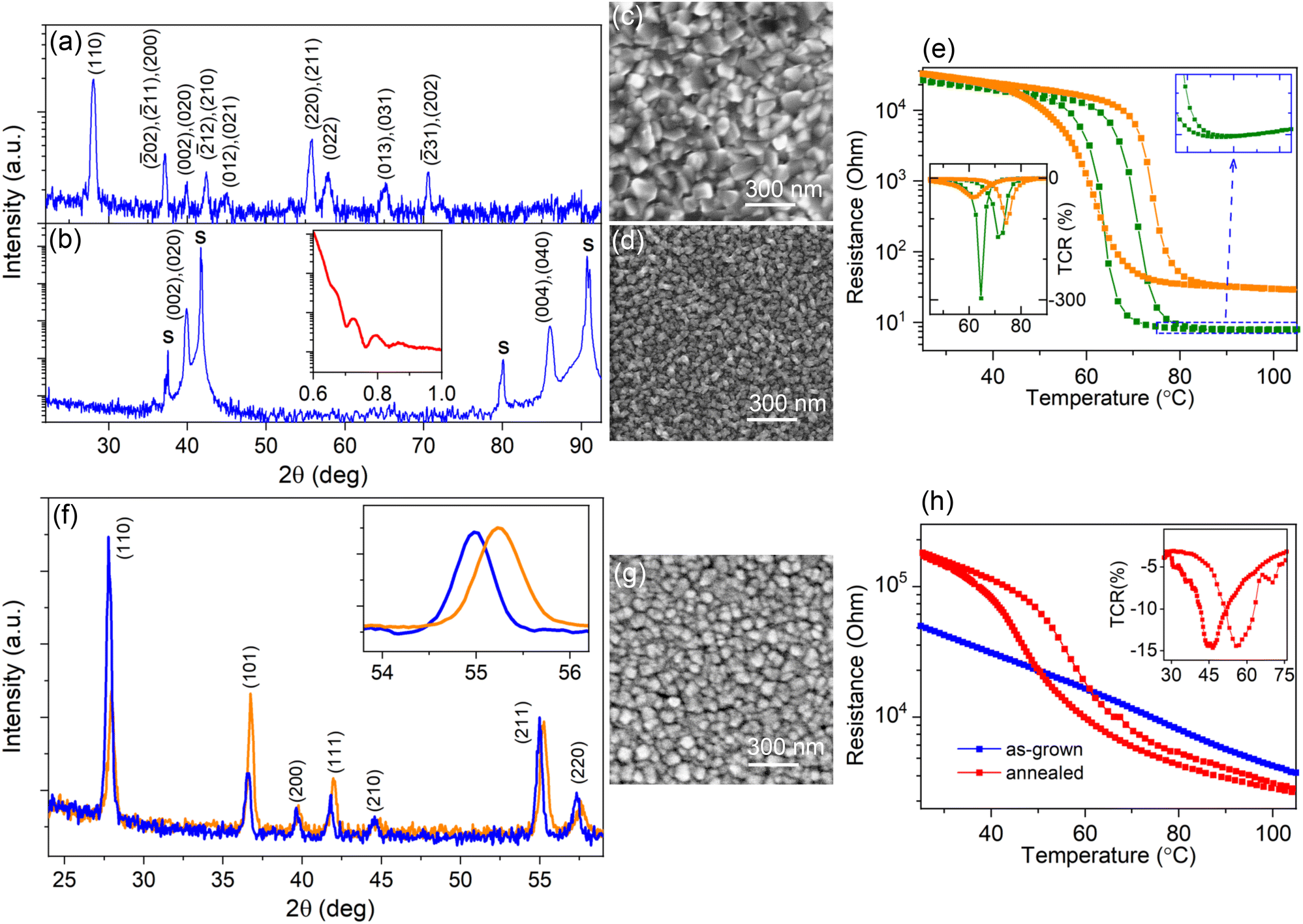 | ||
| Fig. 1 Characterization of VO2 and V1−x TixO2 thin films. XRD patterns of VO2 films grown on (a) fused quartz and (b) Al2O3(0001) substrates (the sapphire peaks are denoted by s); the inset in (b) shows the XRR oscillations of the 83 nm-thick film. SEM images of VO2 films grown on (c) fused quartz and (d) Al2O3(0001) substrates. (e) Temperature-dependent resistance of VO2 films grown on Al2O3(0001) (olive) and fused quartz (orange) substrates; the insert shows the thermal coefficients of resistance, TCR(T) = 100% × (1/R)(dR/dT). The magnified area in (e) demonstrates the metallic conductivity of the VO2 film grown on Al2O3(0001). (f) XRD patterns of two V1−xTixO2 films with x1 = 0.26 (orange) and x2 = 0.43 (blue); the inset demonstrates shifting of the (211)-peak with x. (g) SEM image of 180 nm-thick V0.65Ti0.35O2 films grown on fused quartz substrate. (h) Temperature-dependent resistance of as-grown (blue) and annealed (red) at 530 °C for 1 hour V0.65Ti0.35O2 film; the inset shows TCR(T) of the annealed film. | ||
SEM images of the VO2 films grown under the optimized conditions on fused quartz and Al2O3(0001) substrates are presented in Fig. 1c and d, respectively. Both surfaces are composed of densely packed grains, but their average sizes are quite different: they reach D ∼ 120 nm in the polycrystalline film and D ∼ 40 nm in the single-oriented film of the same thickness. The smoother surface of the oriented film on sapphire allowed us to determine the film thickness of d ∼ 83 nm by XRR (the insert on Fig. 1b). The R(T) curves shown in Fig. 1e reveal the same TMI = 68 °C both for the polycrystalline and the single-oriented films; here TMI was determined as a middle temperature between TCR(T) minima (see the inset in Fig. 1e). However, the width, sharpness, and amplitude of the hysteresis loops are predictably different because of the large contribution of irregular grain boundaries in the polycrystalline material. The obtained TMI value exactly fits the tabulated value for pristine VO2.19 The observed metallic behavior above TMI in the single-oriented film (see the zoomed area of the R(T) curve in Fig. 1e) confirms the achievement of pure-phase VO2 synthesis.
Titanium is less prone to phase variation, displaying a valence state of 4+ for all oxygen pressures that are higher than the minimum value required for stoichiometric TiO2 formation. Therefore, before V1−xTixO2 deposition, we verified the formation of TiO2 under the optimal conditions for synthesizing pure-phase VO2, i.e. under ∼0.4% oxygen in an Ar + O2 atmosphere. The obtained films were insulating with a sheet resistance above 108 Ω. Fig. S1† presents the results of characterization for a TiO2 film grown on a fused quartz substrate. The AFM image in Fig. S1a† demonstrates the typical surface of a polycrystalline film comprising grains with an average size of D ∼ 60 nm. This surface morphology was sufficiently smooth to develop XRR oscillations (see Fig. S1b†) and to determine the film thickness d = 34 nm. All XRD peaks in Fig. S1c† belong to the rutile TiO2 structure, confirming thus the formation of TiO2 under O2 content of 0.4%.
To fabricate V1−xTixO2, a specified quantity of the V precursor was replaced with the Ti precursor, maintaining the integral molarity of the mixed precursor solutions and all other growth conditions constant. A fast cooling rate of ∼100 °C min−1 was applied after film growth to freeze out the metastable state of the obtained solid solution. Fig. 1f shows the XRD patterns of the two V1−xTixO2 films with different Ti contents. One can see that, regardless of the Ti/V precursor ratio, XRD reveals peaks belonging to the solid solution only. The texture shifts towards the (110)-orientation with an increase in the Ti-content, but all peaks correspond to the rutile structure and are located between those seen for pristine VO2 and TiO2. This result is in line with rutile structure formation at x > 0.2 in the bulk polycrystals.7 According to Vegard's law, the compositions of the V1−xTixO2 films in Fig. 1f correspond to x1 = 0.26 and x2 = 0.43. By tuning the Ti/V ratio we obtained the solid solution with nominal value of x = 0.35 required for further SD processing. In Fig. 1g the SEM image shows the surface morphology of a 180 nm-thick V0.65Ti0.35O2 film with an average grain size of D ∼ 120 nm. The EDX spectrum in Fig. S2† corresponds to the metal stoichiometry of V0.66Ti0.34, confirming thus the compositional analysis performed by XRD.
The SD was then activated by a step-by-step increase in either the temperature or duration of post-growth annealing. We observed that the surface morphology and average composition of the solid solution films remained unchanged (not shown) during all annealing cycles. However, the R(T) dependence changed after exposure to 530 °C for 1 h, transforming from a gradual dependence into a hysteresis loop, as shown in Fig. 1h. The observed resistance switching suggests the onset of the MI transition in the V0.65Ti0.35O2 film owing to the appearance of the V-rich phase. It is worth noting that our attempts to further increase either the temperature or duration of annealing resulted in deterioration of the R(T) hysteresis loop. In comparison with the R(T) dependence in Fig. 1e for the optimized VO2, the resistance switching of annealed V0.65Ti0.35O2 in Fig. 1h is shifted towards a lower temperature, implying an essential difference between the emerged V-rich phase and the pure-phase VO2.
3.2 TEM analysis
The microstructures of the as-grown and annealed V0.65Ti0.35O2 films were analyzed by TEM and compared with that of pure VO2 polycrystalline film. The top row in Fig. 2 presents the plan-view BF STEM images of VO2 (a), as-grown (b), and annealed (c) V0.65Ti0.35O2. In contrast to VO2, a periodic alternation of bright and dark stripes appeared in both V0.65Ti0.35O2 samples. The cross-sectional BF STEM image shown in Fig. 2d also reveals the striped microstructure of the annealed V0.65Ti0.35O2 film. The V- and Ti-rich layers appear in the BF images as dark and bright strips, respectively. In bulk polycrystalline materials, the alternation of bright and dark bands indicates the separation of the V- and Ti-rich phases that emerge as a result of SD.7 Note that the striped microstructure can be observed by TEM only in the grains for which the direction of compositional modulation coincides with the image plane. In otherwise oriented grains, the elemental contrast is screened by the overlapping layers. By choosing correctly oriented grains, the estimated thickness of the individual layers is equal to ∼8 nm for the Ti-rich layers and ∼12 nm for the V-rich ones. The observed layered nanostructures contain stacking faults and “curved” layers, which result from the irregular shape of the crystallites and a limited number of layers embedded in the nano-sized grains.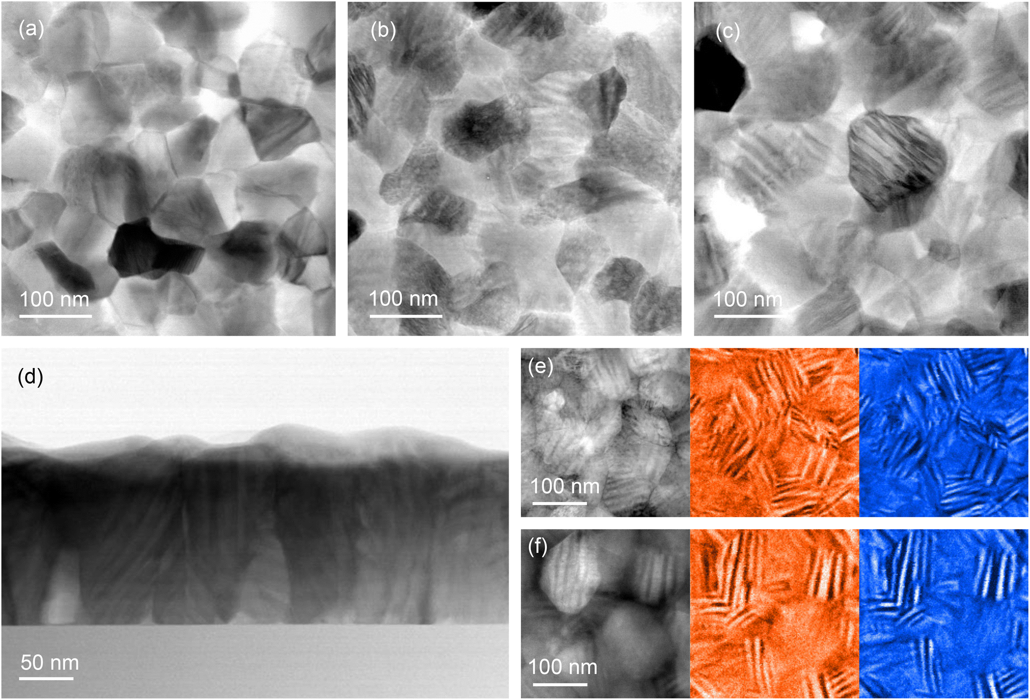 | ||
| Fig. 2 TEM analysis of VO2 and V0.65Ti0.35O2 films grown on fused quartz substrates. Plan-view BF STEM images of (a) VO2, (b) as-grown, and (c) annealed V0.65Ti0.35O2 films. (d) Cross-sectional BF STEM image of annealed V0.65Ti0.35O2 films. HAADF-STEM images and respective EELS maps of as-grown (e) and annealed (f) V0.65Ti0.35O2 films; V is marked as orange and Ti as blue. | ||
Thus, TEM analysis confirmed the realization of SD in the small crystallites of thin polycrystalline films. Moreover, it was revealed that a layered nanocomposite also forms in the as-grown V0.65Ti0.35O2 film, pointing out that SD occurs even during film growth. The presence of a layered structure signifies the spinodal nature of phase separation during growth; the alternative process of phase separation through nucleation and growth can only yield nanodot or nanopillar-embedded composites due to the isotropy of adatom surface mobility on the amorphous substrates. The development of SD during film growth has been predicted theoretically37 and observed experimentally in epitaxial (V,Ti)O2 films.18 However, the observed here nanoscale phase separation in the as-grown V0.65Ti0.35O2 contradicts the gradual R(T) behavior in the as-grown sample (see Fig. 1h), apparently contrasting with a robust hysteresis loop appeared after the annealing. The lack of resistance switching in the as-grown films can be rationalized by comparing the elemental compositions of the V- and Ti-rich layers before and after annealing. HAADF STEM images with corresponding the EELS elemental maps are shown in Fig. 2e and f for the as-grown and annealed V0.65Ti0.35O2 films, respectively. The bright and dark strips in the HAADF STEM image correspond to the V (red) and Ti (blue) areas, respectively, in the EELS elemental maps. The Ti content in the as-grown film corresponds to x = 0.41 in the Ti-rich layers and x = 0.24 in the V-rich ones. After annealing, the degree of compositional modulation becomes notably higher: x = 0.45 (Ti-rich) and x = 0.19 (V-rich). It was established7 that the value of x < 0.2 is necessary for efficient V–V dimerization, which is an essential prerequisite of the MI transition in VO2. Thus, the observed compositional modulation in the as-grown film, i.e. V0.76Ti0.24O2, is insufficient for V–V dimerization and the onset of MI transition. Post-growth annealing resulted in the formation of V0.81Ti0.19O2 layers with a sufficiently high concentration of V for the manifestation of a pronounced MI transition in R(T) dependence.
3.3 XRD analysis
XRD patterns in Fig. S3† reveal a broadening of the (101), (111), and (211) peaks after post-growth annealing, whereas the (110), (200), and (210) peaks remain unchanged. Because broadening was detected only for (hkl)-peaks with l = 1, the compositional modulation is directed along the cR-axis7 and is independent of the grain orientations. In Fig. 3 a detailed XRD pattern near the broadened (101)-peak of V0.65Ti0.35O2 is shown together with the corresponding peaks of the VO2 and TiO2 films. Two important changes induced by annealing can be observed: (1) the (101)-peak shifts toward a larger 2θ-angle; and (2) two small peaks appear symmetrically on both sides of the main (101)-peak. The observed shift indicates either a change in the film composition or a strained state of the layered nanocomposite. According to the EDX data, the average film composition did not change after the annealing. Therefore, we can attribute this shift to a decrease in the c-lattice parameter from 0.2250 to 0.2247 nm, which indicates residual compressive strain. The reason for compression is the coherent interfacing of the V- and Ti-rich layers along the a(b)-axis in the presence of a lattice mismatch (0.86% between pristine VO2 and TiO2). Coherent interfacing results in compressive and tensile strains along the cR-axis in the V- and Ti-rich layers, respectively. The overall shift of the main peak to a larger 2θ-angle means that shrinking cR in V-rich layers overcomes its expansion in Ti-rich layers. Note that the as-grown V0.65Ti0.35O2 film appears to be unstrained, and this state coexists with a level of compositional modulation that is insufficient to exhibit a hysteresis loop in the R(T) dependence.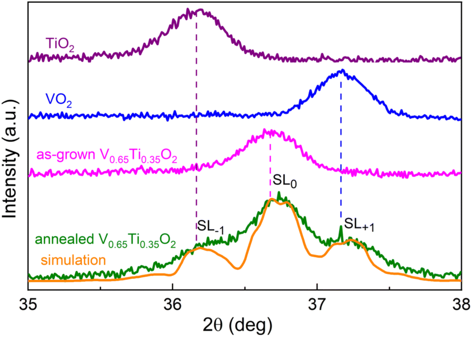 | ||
| Fig. 3 Normalized XRD patterns next to the (101) peaks of TiO2 (purple), VO2 (blue), as-grown (magenta), and annealed (olive) V0.65Ti0.35O2 films grown on fused quartz substrates. Simulated XRD (orange) of polycrystalline film with grains comprised V0.81Ti0.19O2/V0.55Ti0.45O2 superlattices. The positions of the (101) peaks are indicated by the vertical dashed lines in the respective colors. | ||
The appearance of two minor peaks after annealing (Fig. 3) was more intriguing. In principle, by stopping the SD process at the initial stage, it is possible to acquire an XRD pattern comprising both the initial peak of the solid solution and two minor peaks, which correspond to the incipient V- and Ti-rich phases. However, TEM analysis revealed a significant degree of phase separation even before and, especially, after the annealing of V0.65Ti0.35O2. Moreover, the angular distance between the main and minor peaks is too large; the minor peak at a larger 2θ-angle corresponds to a compressed pure phase of VO2, but the EELS analysis established a V-rich phase composition of V0.81Ti0.19O2. Therefore, another origin for the minor peaks must be supposed. Because the minor peaks appear at equal distances from the main one, we suppose that these peaks represent satellites SL−1 and SL+1 of the main superlattice peak SL0. That is, the appearance of minor peaks points to the right periodicity of V0.81Ti0.19O2 and V0.55Ti0.45O2 layers. By applying Schuller's formula38 for superlattices Λ = λ/(sinθn − sinθn−1), a superlattice period Λ = 20.6 nm was determined. This value agrees very well with the sum of the V- and Ti-rich layer thicknesses, i.e. 12 + 8 = 20 nm, as observed by TEM (Fig. 2). By numerically fitting the XRD patterns, we estimated the individual values of the residual strains in the V- and Ti-rich layers. The best agreement between the simulated and experimental curves in Fig. 3 was achieved at the same value of the lattice strain parameter, Δc/c = 0.01 ÷ 0.014, in both layers. Considering that compressed V-rich layers are 1.5 times thicker than tensile Ti-rich layers, the average lattice parameter of the whole SL decreases and the position of the central SL0 peak shifts toward a higher 2θ-angle.
3.4 Raman analysis
Despite the considerable compositional modulation, SL peaks were absent in the as-grown V0.65Ti0.35O2 films. Therefore, along with the quantitative enhancement of the compositional modulation revealed by TEM, post-growth annealing results in a distinct structural transformation. Raman spectroscopy allows us to elucidate this transformation. Fig. 4 shows the Raman spectra of a V0.65Ti0.35O2 film before and after annealing, as well as the spectrum of a pure-phase VO2 film and reference data for rutile TiO2.39 Almost all phonon modes of monoclinic VO240 were identified in the spectrum of the VO2 film. The spectrum of the annealed V0.65Ti0.35O2 film reproduces most of the VO2 modes, but with a shift towards smaller wavenumbers, e.g., the Ag mode shifts from 613 cm−1 to 602 cm−1. This shift is caused by the formation of a solid solution because the replacement of V with Ti increases the bond length at almost identical binding energies of the Ti–O and V–O bonds.41
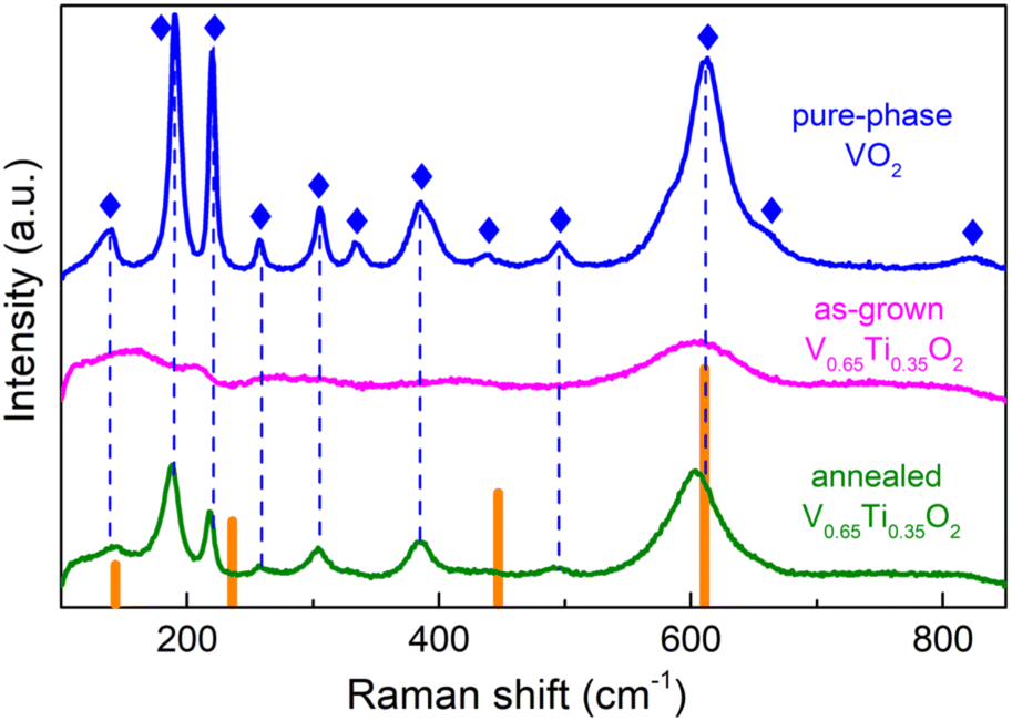 | ||
| Fig. 4 Room-temperature micro-Raman spectra acquired on the pure-phase VO2 film (blue), as-grown (magenta), and annealed (green) at 530 °C for 1 hour V0.65Ti0.35O2 films grown on fused quartz substrates. Diamonds indicate the tabulated VO2 modes. The vertical dashed lines show the correspondence between the lines in the VO2 and V0.65Ti0.35O2 spectra. The orange strips denote the positions and relative intensities of rutile TiO2 lines. | ||
The Raman spectrum of the as-grown V0.65Ti0.35O2 film, which lacks almost all phonon modes, differs drastically from those measured for VO2 and annealed V0.65Ti0.35O2 films. It consists of only a 602 cm−1 mode, which is broader and weaker than that of the annealed V0.65Ti0.35O2 film. Because XRD reveals robust crystallinity in the as-grown film, we cannot attribute such strong damping of almost all phonon modes to an amorphous state of V0.65Ti0.35O2. It is likely that the observed contradiction between XRD and Raman spectroscopy is caused by the different probing scales of these methods. Raman spectroscopy is sensitive to the local atomic-scale coordination, which is determined mainly by the nearest neighbors and to a lesser extent by the next to nearest-neighbor atoms, i.e. the probing scale is ∼1–2 unit cells.42 The coherence scattering length of XRD in polycrystalline materials is limited by the size of the crystallites. By applying Scherrer's formula L = 0.9λ/βcosθ, where L is the crystallite size, λ is the X-ray wavelength, β is the full width at half maximum of the diffraction peak, the estimated average grain size in the V0.65Ti0.35O2 film is L ≈ 50 unit cells. This size exceeds the probing scale of Raman spectroscopy by many times. Therefore, the observed contradiction can be explained by the difference between the local atomic structure and long-range or mesoscopic structure (crystallite). The local disorder in the metastable V0.65Ti0.35O2 solid solution stems from the inhomogeneous distribution of Ti and V atoms during growth. The alloying-induced disorder was frozen by the fast cooling after film growth, producing thus numerous local microphases with various arrangements of V–Ti atomic chains. Raman spectroscopy is able to detect vibrational modes from similar micro-phases developing in a random solid solution.43 In our case, the overlapping of slightly displaced vibrational modes from different microphases results in the observed broadening of the most intensive Ag-peak and damping of the rest of peaks with a smaller intensity. Hence, the results of Raman spectroscopy allowed us to conclude that upon annealing, the random solid solutions in the V- and Ti-rich layers underwent a structural transformation into short-range ordered states.
3.5 Optical transmittance
Using R(T) measurements, we detected the onset of the MI transition in the V0.65Ti0.35O2 film after annealing. However, percolative transport through the two-phase nanocomposite, where only V-rich layers undergo the MI transition, causes smearing of the hysteresis loop in R(T). Optical transmittance measurements allowed us to uncover the characteristics of the MI transition in the V-rich phase and to elucidate the thermochromic properties of the (V,Ti)O2-nanocomposite. Fig. 5 presents the temperature-dependent Vis–NIR optical transmittance of a pure VO2 film in comparison with the as-grown and annealed V0.65Ti0.35O2 films.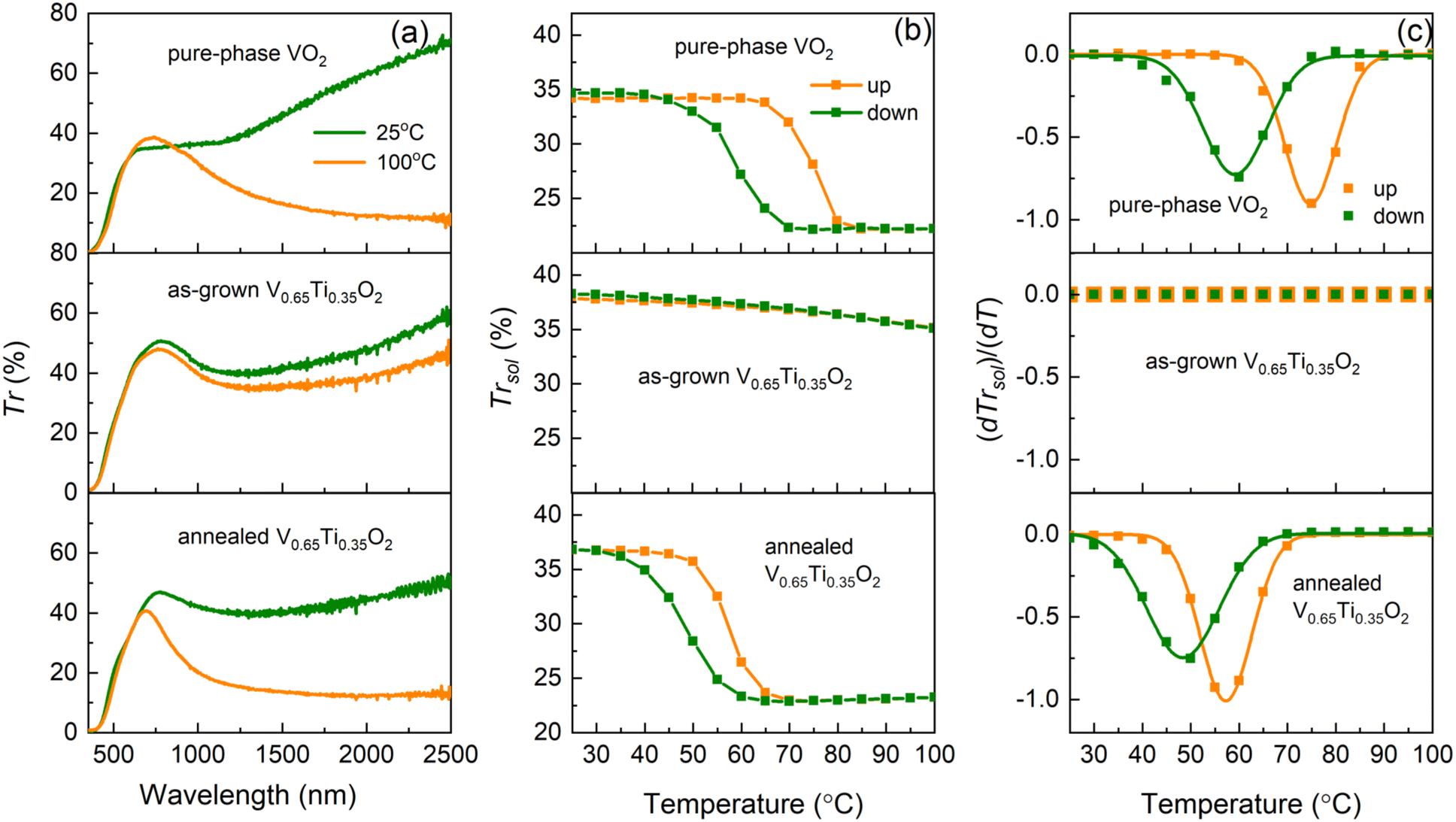 | ||
| Fig. 5 Optical properties of 83 nm-thick VO2 films (top panels) in comparison with 180 nm-thick as-grown (middle panels) and annealed (bottom panels) V0.65Ti0.35O2 films all deposited on fused quartz substrates. (a) Vis–NIR transmittance spectra at 25 and 100 °C. (b) Temperature-dependent integral solar transmittance in the 250 ÷ 2500 nm range of wavelengths. (c) Derivatives of integral solar transmittance: experimental points and Gaussian fittings. | ||
The Vis–NIR transmittance spectra in Fig. 5a were measured well below (25 °C) and above (100 °C) the standard TMI = 68 °C for pristine VO2. The spectra of the VO2 film demonstrate a typical transition-induced change in the NIR transmittance, ΔTr = 38% at 1700 nm, for a film thickness d = 83 nm. The as-grown 180 nm-thick V0.65Ti0.35O2 film exhibited a negligible change, ΔTr = 7%. However, the emergence of MI transition after annealing led to an increase in ΔTr to 29%. Fig. 5b shows the temperature-dependent integral solar transmittance, ΔTrsol, for wavelengths λ = 250–2500 nm for the VO2 and V0.65Ti0.35O2 films shown in Fig. 5a. The main MI transition characteristics (TMI, width, and amplitude of the hysteresis loop) are shown in Fig. 5c by plotting the derivative dTrsol/dT and fitting the curves using Gaussians. Here, TMI is determined as the middle temperature between the derivative minima for the heating and cooling curves. The pure VO2 film demonstrated a tabulated MI transition temperature, TMI = 68 °C, confirming the value evaluated from R(T) in Fig. 1e. The solar modulation ability, ΔTrsol = 12%, and width of the thermal hysteresis loop, ΔTMI = TMI (heating) − TMI (cooling) = 16 °C, agree well with those reported for high-quality polycrystalline VO2 films of comparable thickness.44 The as-grown V0.65Ti0.35O2 film demonstrates a lack of hysteresis behavior similar to the R(T) measurements, exhibiting a weak gradual decrease of Tsol with temperature and a low solar modulation ΔTrsol = 3%, which appears because of the variation in the optical constants with temperature. In contrast, the onset of the MI transition in the V-rich layers after annealing led to a pronounced hysteresis loop, which demonstrated a reduced TMI of 53 °C, a decreased ΔTMI of 9 °C, and an enhanced ΔTrsol of 14%.
The observed change in ΔTrsol can be interpreted as a result of the increased VO2 content in the 180 nm-thick V0.65Ti0.35O2 film compared to that in the 83 nm-thick pure-phase VO2 film. However, the simultaneous decrease in TMI and ΔTMI can only be caused by compressive strains in the V-rich layers because simple alloying of VO2 with TiO2 leads to an extended transition at elevated TMI.45 The emergence of strain-enhanced optical characteristics after annealing was in full agreement with the formation of a strained superlattice-like microstructure, as revealed by XRD. The lack of the substrate clamping effect causes the independence of interfacial strains on the grain orientation and leads to a reduction of TMI by 15 °C, which substantially exceeds the 5–6 °C reduction observed in the presence of the clamping effect in epitaxial films.15
Despite the ∼40% excess in VO2 content, the V0.65Ti0.35O2 and VO2 films possess almost the same values of Trlum, 29.0 and 28.9%, respectively. According to the nanothermochromic concept, VO2 nanoparticles embedded in a transparent dielectric host provide a higher Trlum than VO2 films of an equivalent thickness.25 In our case, the layers of a more transparent TiO2-rich phase produced the nanothermochromic effect, maintaining Trlum at the same value despite an increase in the equivalent VO2 thickness.
3.6 Discussion
We established that spinodal decomposition can be performed in small grains of thin polycrystalline V1−xTixO2 films in the same manner as in bulk materials and epitaxial films. In addition to a basic similarity, two essential differences were observed: (1) SD develops simultaneously with film growth, producing a significant phase separation in the as-grown V0.65Ti0.35O2 films, and (2) post-growth annealing results in the formation of strained superlattice-like (V,Ti)O2 nanostructures.An in situ SD during film growth has already been observed in epitaxial (V,Ti)O2 films when the cR-axis coincides with the film growth direction.18 In our case, the direction of compositional modulation was irrelevant to the grain orientation, and the SD was identical to that in the bulk materials. We suppose that enhanced surface adatom diffusion is responsible for SD during growth, whereas bulk diffusion occurs under post-grown annealing. The enhancement of surface diffusion stems from the main peculiarities of MAD growth: (1) being a chemical technique, MAD operates under near-equilibrium growth conditions, promoting surface diffusion; (2) the pyrolysis of precursors such as β-diketonates of V and Ti is an exothermic reaction, resulting in an additional increase in the surface temperature, which leads to an extra enhancement of surface diffusion. However, adatom diffusion is kinetically limited by deposition rate. As a result, phase separation during growth was incomplete, yielding an insufficient concentration of V to achieve the MI transition in V-rich layers. Moreover, Raman spectroscopy revealed a disordered state in the as-grown solid solutions, with an inhomogeneous local distribution of V and Ti atoms. Such random solid solutions possess diffused interfaces; thus, they are inconsistent with the formation of strained nanocomposites via coherent interfacing between layers. Therefore, neither superlattice-like nanostructure nor MI transition were observed in the as-grown V0.65Ti0.35O2 films.
The activation of bulk diffusion by post-growth annealing results in predictable strengthening of the compositional modulation, yielding also strained superlattice-like nanostructures. This is the most remarkable feature revealed by XRD analysis in the thin polycrystalline V0.65Ti0.35O2 films. The corresponding transformation of the optical properties, i.e. a simultaneous decrease in TMI and ΔTMI, confirms the strained state after annealing. In principle, the formation of SLs is the conventional termination step of the SD process.4 Nevertheless, suitable conditions for SL formation are hardly accessible because of (1) the pinning of compositional waves at various structural imperfections and (2) the development of new phases by concurrent processes of nucleation. We suppose that in our case, a fine grain size, D ∼ 30–100 nm, facilitates the formation of superlattices. In bulk materials, the result of SD is determined by the superposition of numerous compositional waves initiated in different parts of a large crystalline grain, D > 0.5 μm for bulk polycrystals7 or mm-size single crystals.9 For a grain size of only several tens of nanometers, it is plausible to suppose that a single compositional wave propagates over the entire crystallite, forming a superlattice-like structure of just a few periods.
As a moderate SD level has been obtained during film growth, it raises the question of whether a higher level of compositional modulation can be achieved during growth without a considerable increase in substrate temperature. This is a key challenge for the practical application of (V,Ti)O2-based nanocomposites as thermochromic coatings because the thermal budget of smart window fabrication is limited by the glass transition temperature. We obtained an enhanced surface adatom mobility during growth at Tsub = 470 °C. To activate bulk diffusion, we applied post-growth annealing at 530 °C, exceeding thus the deposition temperature by 60 °C only. We believe that further enhancement of surface diffusion during film growth can be achieved either (1) by overcoming the kinetic limitation using a reduced deposition rate or (2) by preventing the formation of foreign phase inclusions, which interrupt the diffusion flux. The latter stems from the fact that the SD in bulk polycrystals can be activated at temperatures as low as 400 °C (ref. 7) and the most probable structural defects in the VO2–TiO2 system are related to VO2 off-stoichiometry. Thus, in our case, we can assign the necessity for higher temperatures to the unbalanced cation–anion stoichiometry, owing to the partial replacement of V by Ti. Indeed, the degree of V oxidation may be reduced because a higher oxygen consumption is required for the utilization of organic residues36 for the Ti precursor, Ti(O-i-Pr)2(TMHD)2, which contains four organic ligands, in contrast with only two ligands in the V-precursor, OV(acac)2. According to the Ellingham diagrams, a large difference in the formation energies favors TiO2 stabilization over VO2 in the case of an oxygen deficiency.
Through optical measurements, we revealed a simultaneous improvement in several thermochromic parameters. These enhancements encompass the reduction of TMI and ΔTMI, as well as the presence of the nanothermochromic effect due to more transparent Ti-rich layers. Well-established strategies are often effective in enhancing a specific parameter only, however, this improvement generally comes at the cost of degradation in the others.46 For instance, the incorporation of doping elements, particularly W, is undoubtedly an effective strategy for reducing TMI to the desired range of 20 ÷ 25 °C, but it results in a broader transition. Similarly, nanothermochromism is a superior way for increasing luminous transmittance up to the required values of Trlum > 60%, but this method also fails to address the issue of switching behaviour. By comparing our proposed approach with the aforementioned strategies, we can deduce that SD-assisted formation of strained (V,Ti)O2-based nanocomposites is a promising method for the development of thermochromic coatings. While thermochromic parameters (TMI = 53 °C, ΔTrsol = 14%, Trlum = 29%) achieved in this study are still quantitatively insufficient, the demonstrated potential to simultaneously enhance several crucial factors, such as MIT temperature, luminous transmittance, and switching behavior, through a single strategy provides a promising foundation for future research.
The process of spinodal decomposition encounters a notable restriction in the thickness and composition of the resulting layers due to the necessity for preserving initial V1−xTixO2 composition near x = 0.35. This constraint imposes limitations on the potential strain-induced enhancements. Nonetheless, our polycrystalline films have not yet reached the same level of decomposition as one achieved in bulk materials. In order to lower the TMI, it is necessary to achieve a higher degree of compositional modulation during SD-process. We believe that by increasing the compositional modulation and using a heterostrain detached from the substrate, the TMI can be downshifted to the required temperatures. The sharpness and width of the NIR transmittance switching can also be advanced by increasing the compressive strain in the V-rich layers. If the nanothermochromic increase of Trlum by the Ti-rich layers will be insufficient due to limitations on their maximum thickness, a further advance could be achieved by adding a third oxide component, such as ZnO, which is transparent and structurally unmixable with the VO2–TiO2 system. The interrelation between the structure and composition-dependent properties of (V,Ti)O2-based nanocomposites is quite complex, and to fulfill all requirements for thermochromic coatings simultaneously, experimental work on nanocomposite metamaterials will strongly benefit from a predictive numerical simulation of their optical properties.
4 Conclusion
Overall, using spinodal decomposition, we demonstrated the formation of strained superlattice-like nanocomposites in thin polycrystalline films of V0.65Ti0.35O2. Starting during growth with the formation of atomic-scale disordered V- and Ti-rich layers, spinodal decomposition is completed by subsequent post-growth annealing, producing sharp heterointerfaces between the layers and creating a superlattice-like nanocomposite inside crystalline grains. Elastically coupled heterointerfaces between V- and Ti-rich layers generate lattice misfit strains, which compress the VO2-rich phase along the c-axis of the rutile structure and yield a strain-enhanced thermochromism with a simultaneous reduction in the temperature of the MI transition and narrowing of the hysteresis loop. In addition, the layers of the TiO2-rich phase promote luminous transmittance, according to the nanothermochromic concept. However, to meet the strict requirements for thermochromic coatings quantitatively, further improvements must be made based on thorough optimization of the entire fabrication process.Author contributions
A. B. conceived of the original idea and drafted the manuscript. A. B. and O. S. designed the thin film deposition system. O. S. fabricated the samples. O. S. and A. B. carried out the characterizations of the samples. V. R. performed TEM analysis. S. V. carried out XRD analysis. J. W. performed Raman spectroscopy. K. S. performed optical measurements. A. B., O. S., and V. M. contributed to the interpretation of the results. V. M. contributed to the final version of the manuscript and supervised the project. All authors discussed the results and commented on the manuscript.Conflicts of interest
There are no conflicts to declare.Acknowledgements
Funding by the Deutsche Forschungsgemeinschaft via the CRC 1073, project Z02, by STCU project no. 6133, and by NARD(ANCD) project no. 20.80009.5007.12 and the use of equipment in the “Collaborative Laboratory and User Facility for Electron Microscopy” (CLUE) are gratefully acknowledged.References
- G. M. Whitesides and B. Grzybowski, Science, 2002, 295, 2418–2421 CrossRef CAS PubMed.
- Z. Chai, A. Childress and A. A. Busnaina, ACS Nano, 2022, 16, 17641–17686 CrossRef CAS PubMed.
- J. W. Cahn, Acta Metall., 1961, 9, 795–801 CrossRef CAS.
- P. Venezuela, J. Tersoff, J. A. Floro, E. Chason, D. M. Follstaedt, F. Liu and M. G. Lagally, Nature, 1999, 397, 678–681 CrossRef.
- S. Gallardo-Hernández, I. Martinez-Velis, M. Ramirez-Lopez, Y. Kudriatsev, A. Escobosa-Echavarria, S. L. Morelhao and M. Lopez-Lopez, Appl. Phys. Lett., 2013, 103, 192113 CrossRef.
- Y. Horibe, M. Ishimatsu, S. Takeyama, S. Mori, M. Kudo, M. Auchi, M. Tanaka and Y. Murakami, Appl. Phys. Lett., 2019, 115, 232401 CrossRef.
- Z. Hiroi, H. Hayamizu, T. Yoshida, Y. Muraoka, Y. Okamoto, J. Yamaura and Y. Ueda, Chem. Mater., 2013, 25, 2202–2210 CrossRef CAS.
- M. Ogata, K. Kadowaki, M. Ijiri, Y. Takemoto, K. Terashima, T. Wakita, T. Yokoya and Y. Muraoka, J. Eur. Ceram. Soc., 2017, 37, 3177–3183 CrossRef CAS.
- Z. Hiroi, T. Yoshida, J. Yamaura and Y. Okamoto, APL Mater., 2015, 3, 062508 CrossRef.
- Z. Chen, X. Wang, Y. Qi, S. Yang, J. A. N. T. Soares, B. A. Apgar, R. Gao, R. Xu, Y. Lee, X. Zhang, J. Yao and L. W. Martin, ACS Nano, 2016, 10, 10237–10244 CrossRef CAS PubMed.
- Y. Muraoka, F. Yoshii, T. Fukuda, Y. Manabe, M. Yasuno, Y. Takemoto, K. Terashima, T. Wakita and T. Yokoya, Thin Solid Films, 2020, 698, 137854 CrossRef CAS.
- Y. Zheng, Z. Chen, H. Lu, Y. Cheng, X. Chen, Y. He and Z. Zhang, Nanoscale, 2021, 13, 7783–7791 RSC.
- T. Fukuda, Y. Takemoto, T. Wakita, T. Yokoya and Y. Muraoka, Thin Solid Films, 2022, 751, 139210 CrossRef CAS.
- G. Sun, H. Zhou, X. Cao, R. Li, M. Tazawa, M. Okada and P. Jin, ACS Appl. Mater. Interfaces, 2016, 8, 7054–7059 CrossRef CAS PubMed.
- G. Sun, X. Cao, Y. Yue, X. Gao, S. Long, N. Li, R. Li, H. Luo and P. Jin, Sci. Rep., 2018, 8, 5342 CrossRef PubMed.
- Y. Matsuura, F. Yoshii, T. Otsuka, K. Kadowaki, M. Ijiri, Y. Takemoto, K. Terashima, T. Wakita, T. Yokoya and Y. Muraoka, J. Eur. Ceram. Soc., 2018, 38, 5043–5050 CrossRef CAS.
- Y. Muraoka, K. Takeda, Y. Takemoto, T. Wakita and T. Yokoya, Thin Solid Films, 2023, 769, 139749 CrossRef CAS.
- J. Park, G.-Y. Kim, K. Song, S.-Y. Choi and J. Son, NPG Asia Mater., 2019, 11, 1868 Search PubMed.
- F. J. Morin, Phys. Rev. Lett., 1959, 3, 34–36 CrossRef CAS.
- K. Liu, S. Lee, S. Yang, O. Delaire and J. Wu, Mater. Today, 2018, 21, 875–896 CrossRef CAS.
- S. Babulanam, T. Eriksson, G. Niklasson and C. Granqvist, Sol. Energy Mater., 1987, 16, 347–363 CrossRef CAS.
- J. Houska, J. Appl. Phys., 2022, 131, 110901 CrossRef CAS.
- M. E. A. Warwick, I. Ridley and R. Binions, Open J. Energy Effic., 2013, 02, 75–88 CrossRef.
- X. Geng, T. Chang, J. Fan, Y. Wang, X. Wang, Y. Sun, P. Selvarajan, C. Liu, C.-H. Lin, X. Wang, J. Yang, Z. Cheng, K. Kalantar-Zadeh, X. Cao, D. Wang, A. Vinu, J. Yi and T. Wu, ACS Appl. Mater. Interfaces, 2022, 14, 19736–19746 CrossRef CAS PubMed.
- S.-Y. Li, G. A. Niklasson and C. G. Granqvist, J. Appl. Phys., 2010, 108, 063525 CrossRef.
- T. Paik, S.-H. Hong, E. A. Gaulding, H. Caglayan, T. R. Gordon, N. Engheta, C. R. Kagan and C. B. Murray, ACS Nano, 2014, 8, 797–806 CrossRef CAS PubMed.
- Q. Hao, W. Li, H. Xu, J. Wang, Y. Yin, H. Wang, L. Ma, F. Ma, X. Jiang, O. G. Schmidt and P. K. Chu, Adv. Mater., 2018, 30, 1705421 CrossRef PubMed.
- N. B. Aetukuri, A. X. Gray, M. Drouard, M. Cossale, L. Gao, A. H. Reid, R. Kukreja, H. Ohldag, C. A. Jenkins, E. Arenholz, K. P. Roche, H. A. Dürr, M. G. Samant and S. S. P. Parkin, Nat. Phys., 2013, 9, 661–666 Search PubMed.
- B. Zhi, G. Gao, X. Tan, P. Chen, L. Wang, S. Jin and W. Wu, Mater. Res. Express, 2014, 1, 046402 Search PubMed.
- Y. Muraoka and Z. Hiroi, Appl. Phys. Lett., 2002, 80, 583–585 CrossRef CAS.
- Y. Yang, X. Mao, Y. Yao, H. Huang, Y. Lu, L. Luo, X. Zhang, G. Yin, T. Yang and X. Gao, J. Appl. Phys., 2019, 125, 082508 CrossRef.
- A. Belenchuk, O. Shapoval, V. Roddatis, V. Bruchmann-Bamberg, K. Samwer and V. Moshnyaga, Appl. Phys. Lett., 2016, 109, 232405 CrossRef.
- S. Stepanov, J. Appl. Crystallogr., 2021, 54, 1530–1534 CrossRef CAS PubMed.
- H. A. Wriedt, Bull. Alloy Phase Diagrams, 1989, 10, 271–277 CrossRef CAS.
- K. Shibuya and A. Sawa, AIP Adv., 2015, 5, 107118 CrossRef.
- N. Li, Y.-H. A. Wang, M. N. Iliev, T. M. Klein and A. Gupta, Chem. Vap. Deposition, 2011, 17, 261–269 CrossRef CAS.
- I. Daruka and J. Tersoff, Phys. Rev. Lett., 2005, 95, 076102 CrossRef CAS PubMed.
- I. K. Schuller, Phys. Rev. Lett., 1980, 44, 1597–1600 CrossRef CAS.
- H. Ma, J. Yang, Y. Dai, Y. Zhang, B. Lu and G. Ma, Appl. Surf. Sci., 2007, 253, 7497–7500 CrossRef CAS.
- K. Shibuya and A. Sawa, J. Appl. Phys., 2017, 122, 015307 CrossRef.
- Z. Zhang, Y. Gao, L. Kang, J. Du and H. Luo, J. Phys. Chem. C, 2010, 114, 22214–22220 CrossRef CAS.
- E. Liarokapis, Phys. C, 2000, 341–348, 2185–2188 CrossRef.
- M. N. Iliev, V. G. Hadjiev and V. G. Ivanov, J. Raman Spectrosc., 1996, 27, 333–342 CrossRef CAS.
- H.-C. Ho, Y.-C. Lai, K. Chen, T. D. Dao, C.-H. Hsueh and T. Nagao, Appl. Surf. Sci., 2019, 495, 143436 CrossRef CAS.
- Y. Wu, L. Fan, Q. Liu, S. Chen, W. Huang, F. Chen, G. Liao, C. Zou and Z. Wu, Sci. Rep., 2015, 5, 9328 CrossRef CAS PubMed.
- Y. Cui, Y. Ke, C. Liu, Z. Chen, N. Wang, L. Zhang, Y. Zhou, S. Wang, Y. Gao and Y. Long, Joule, 2018, 2, 1707–1746 CrossRef CAS.
Footnotes |
| † Electronic supplementary information (ESI) available. See DOI: https://doi.org/10.1039/d3nr01350b |
| ‡ Present address: GFZ German Research Centre for Geosciences, Telegrafenberg D-14473 Potsdam, Germany. |
| § Present address: IFW Dresden, Helmholtzstraße 20, D-01069 Dresden, Germany. |
| This journal is © The Royal Society of Chemistry 2023 |