
 Open Access Article
 This Open Access Article is licensed under a
 Creative Commons Attribution 3.0 Unported Licence
Effects of post-transfer annealing and substrate interactions on the photoluminescence of 2D/3D monolayer WS2/Ge heterostructures†
Tianyi
Zhang‡
 ab,
Andrew
Voshell‡
c,
Da
Zhou‡
bd,
Zachary D.
Ward
e,
Zhuohang
Yu
ab,
Mingzu
Liu
bd,
Kevin O.
Díaz Aponte
c,
Tomotaroh
Granzier-Nakajima
bd,
Yu
Lei
bdf,
He
Liu
bg,
Humberto
Terrones
e,
Ana Laura
Elías
h,
Mukti
Rana
*c and
Mauricio
Terrones
*abdg
ab,
Andrew
Voshell‡
c,
Da
Zhou‡
bd,
Zachary D.
Ward
e,
Zhuohang
Yu
ab,
Mingzu
Liu
bd,
Kevin O.
Díaz Aponte
c,
Tomotaroh
Granzier-Nakajima
bd,
Yu
Lei
bdf,
He
Liu
bg,
Humberto
Terrones
e,
Ana Laura
Elías
h,
Mukti
Rana
*c and
Mauricio
Terrones
*abdg
aDepartment of Materials Science and Engineering, The Pennsylvania State University, University Park, PA 16802, USA. E-mail: mut11@psu.edu
bCenter for 2-Dimensional and Layered Materials, The Pennsylvania State University, University Park, PA 16802, USA
cDivision of Physics, Engineering, Mathematics and Computer Sciences and Optical Science Center for Applied Research, Delaware State University, Dover, DE 19901, USA. E-mail: mrana@desu.edu
dDepartment of Physics, The Pennsylvania State University, University Park, PA 16802, USA
eDepartment of Physics, Applied Physics and Astronomy, Rensselaer Polytechnic Institute, Troy, NY 12180, USA
fInstitute of Materials Research, Tsinghua Shenzhen International Graduate School, Tsinghua University, Shenzhen 518055, China
gDepartment of Chemistry, The Pennsylvania State University, University Park, PA 16802, USA
hDepartment of Physics, Binghamton University, Binghamton, NY 13902, USA
First published on 29th June 2023
Abstract
The ultraflat and dangling bond-free features of two-dimensional (2D) transition metal dichalcogenides (TMDs) endow them with great potential to be integrated with arbitrary three-dimensional (3D) substrates, forming mixed-dimensional 2D/3D heterostructures. As examples, 2D/3D heterostructures based on monolayer TMDs (e.g., WS2) and bulk germanium (Ge) have become emerging candidates for optoelectronic applications, such as ultrasensitive photodetectors that are capable of detecting broadband light from the mid-infrared (IR) to visible range. Currently, the study of WS2/Ge(100) heterostructures is in its infancy and it remains largely unexplored how sample preparation conditions and different substrates affect their photoluminescence (PL) and other optoelectronic properties. In this report, we investigated the PL quenching effect in monolayer WS2/Ge heterostructures prepared via a wet transfer process, and employed PL spectroscopy and atomic force microscopy (AFM) to demonstrate that post-transfer low-pressure annealing improves the interface quality and homogenizes the PL signal. We further studied and compared the temperature-dependent PL emissions of WS2/Ge with those of as-grown WS2 and WS2/graphene/Ge heterostructures. The results demonstrate that the integration of WS2 on Ge significantly quenches the PL intensity (from room temperature down to 80 K), and the PL quenching effect becomes even more prominent in WS2/graphene/Ge heterostructures, which is likely due to synergistic PL quenching effects induced by graphene and Ge. Density functional theory (DFT) and Heyd–Scuseria–Ernzerhof (HSE) hybrid functional calculations show that the interaction of WS2 and Ge is stronger than in adjacent layers of bulk WS2, thus changing the electronic band structure and making the direct band gap of monolayer WS2 less accessible. By understanding the impact of post-transfer annealing and substrate interactions on the optical properties of monolayer TMD/Ge heterostructures, this study contributes to the exploration of the processing–properties relationship and may guide the future design and fabrication of optoelectronic devices based on 2D/3D heterostructures of TMDs/Ge.
Introduction
Monolayers of two-dimensional (2D) semiconducting transition metal dichalcogenides (TMDs) are attractive candidates for next-generation electronics and optoelectronics, owing to a plethora of impressive physical properties including large on–off ratios, strong and tunable optical absorption/emission, and large excitonic effects.1–4 Dangling bond-free TMD surfaces further permit their van der Waals (vdW) stacking with many surfaces or substrates regardless of their dimensionality. This unique feature opens up the capability of effectively engineering properties of 2D TMDs by designing 2D/nD (n = 0, 1, 2, and 3) heterojunctions with desirable material combinations, leading to emerging functionalities.5–7 For example, by either directly synthesizing or mechanically transferring monolayer TMDs on target 3D semiconducting substrates (e.g., silicon (Si), gallium nitride (GaN), germanium (Ge)), 2D/3D semiconducting heterostructures have been prepared, creating a boom in a wide variety of device applications, such as tunnel diodes,8,9 tunnel field-effect transistors,10 photovoltaics,11,12 and photodetectors.13,14Among different types of 2D/3D semiconducting heterostructures, monolayer TMDs/bulk Ge has emerged as an interesting one for optoelectronic applications. Specifically, while monolayer TMDs have demonstrated excellent photoresponsivity, their photoresponse is mainly limited to within the visible range because of their relatively large intrinsic band gap (∼1.6–2.0 eV).15,16 In comparison, Ge is a commonly used 3D semiconducting substrate with an indirect band gap of ∼0.66 eV, which exhibits high mobility and large infrared (IR) absorption, especially suited for IR-related applications.17,18 Thus, by constructing 2D/3D vertical heterostructures using TMD/Ge, one can take advantage of the complementary optical properties of TMDs and Ge, so that functional devices such as sensitive IR photodetectors can be fabricated accordingly. For example, photodetectors based on multilayer WS2/Ge heterojunctions with an ultrathin AlOx interfacial layer have been constructed, exhibiting high photoresponsivity (634.5 mA W−1), high specific detectivity, ultrafast photoresponse, and ultrabroadband detection ranging from deep ultraviolet to mid-wave IR (200 nm–4.6 μm).13 In another report, an ultrasensitive near-IR detector based on few-layer MoTe2/Ge has also been fabricated by applying an ultrathin GeO2 interfacial layer to reduce the reverse current and enhance the photoresponsivity.14
Despite these recent studies demonstrating that TMD/Ge heterostructures are promising candidates for optoelectronics, the investigated TMD materials are usually multilayered, and study on the relationship between preparation methods and optical properties of this 2D/3D system is still in its infancy. For example, it remains unclear how sample preparation conditions and substrate interactions affect the photoluminescence (PL) properties of monolayer TMDs on Ge. In this context, we fabricated 2D/3D WS2/Ge heterostructures by transferring chemical vapor deposition (CVD)-grown WS2 monolayers onto the surfaces of Ge(100). Effects of the post-transfer Ar/H2 annealing process on WS2/Ge interface morphology and optical properties were studied by atomic force microscopy (AFM) and PL spectroscopy. Furthermore, we performed a comparative study of temperature-dependent PL responses of as-grown WS2, WS2/Ge, and WS2/graphene/Ge heterostructures. Our results indicate that the WS2/Ge system exhibits a large PL quenching (∼500×) when compared to that of the as-grown WS2 on SiO2/Si, and this PL quenching effect becomes even more prominent in the 2D/2D/3D heterostructures of WS2/graphene/Ge. Density functional theory (DFT) calculations,19 including vdW corrections (DFT-D2)20 and hybrid functional HSE0621 simulations were performed to understand the electronic interaction between WS2 and Ge. It is found that WS2 monolayers interact strongly with Ge(100) and this leads to a reduced interlayer separation, though keeping the vdW interaction without forming a chemical bond. Our work helps to establish the structure–processing–property relationship of TMDs/Ge heterostructures by illustrating the roles of post-transfer annealing and sample–substrate interaction, which may provide useful information for the future fabrication of such 2D/3D optoelectronics using the 2D layer transfer technique.
Results and discussion
Preparation of monolayer WS2/Ge heterostructures
Monolayer WS2 was first synthesized via an atmospheric pressure chemical vapor deposition (APCVD) method.22 As schematically shown in Fig. 1a, the APCVD process involves the use of WO3 and S powders as tungsten and sulfur sources, respectively, and NaBr as a growth promoter (see details in the Methods section).23 The synthesis was carried out at 825 °C for 10 min, and the heating temperature ramps for the metal precursor and S powder are shown in Fig. 1b. To prepare WS2-based 2D/3D heterostructures, we utilized a cellulose acetate (CA)-assisted wet-transfer approach to lift-off as-grown WS2 monolayers and place them onto undoped Ge(100) (Fig. 1c), which had been found to yield improved surface cleanliness and reduced wrinkles/cracks when compared to conventional wet-transfer methods.24 The successful transfer of WS2 monolayers on Ge(100) was verified by optical microscopy imaging and fluorescence imaging, as shown in Fig. 2a and Fig. S1 in the ESI.† Raman spectroscopy characterization also demonstrated the characteristic vibrational modes from both WS2 monolayers and Ge (Fig. S2†), further indicating the formation of WS2/Ge heterostructures. It should be noted that the Raman intensities of characteristic E′ and A′1 modes of WS2 monolayers are significantly lower (∼15 times) for WS2/Ge heterostructures when compared to those of as-grown WS2 on SiO2/Si. This may be explained by the optical interference and absorption effects that lead to substrate-dependent Raman enhancement factors, which have already been observed in monolayer TMDs on various substrates.25,26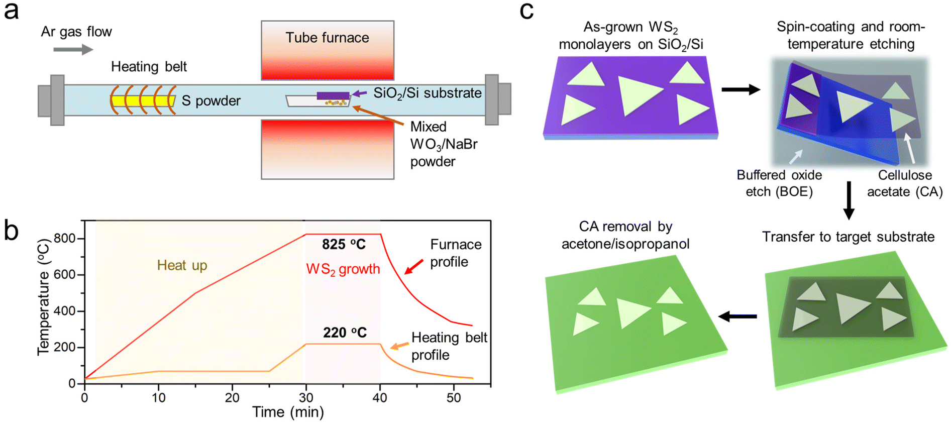 | ||
| Fig. 1 Synthesis and transfer of WS2 monolayers for preparing WS2/Ge heterostructures. (a) Schematic of the APCVD setup for synthesizing WS2 monolayers on SiO2/Si. (b) Furnace and heating belt temperature profiles during the synthesis process. (c) Step-by-step schematics of the wet-transfer of WS2 onto target substrates using a cellulose acetate-assisted approach. | ||
 | ||
| Fig. 2 Effects of post-transfer annealing on the PL and surface morphology of WS2/Ge heterostructures. (a) Optical image of monolayer WS2 transferred on Ge. Due to a relatively weak optical contrast, the edges of WS2 are marked with black dashed lines for clarity. (b) A comparison of PL spectra of as-grown monolayer WS2, as-transferred WS2/Ge, and annealed WS2/Ge. WS2/Ge heterostructures display prominent PL intensity quenching compared to as-grown WS2. (c) PL intensity mapping of as-transferred WS2/Ge and (d) annealed WS2/Ge at 1.98 eV, corresponding to the optical band gap of monolayer WS2. (e) AFM topography image of as-transferred WS2/Ge and (f) the corresponding surface height profile along the white dashed line in (e). (g) AFM topography image of annealed WS2/Ge and (h) the corresponding surface height profile along the white dashed line in (g). | ||
Effects of post-transfer thermal annealing
Sample preparation conditions can often affect the optical properties of TMD-based heterostructures. Since the preparation of 2D/3D WS2/Ge(100) heterostructures involves a wet-transfer process, it is inevitable that contaminants and trapped water molecules are introduced at their interface, which may lead to undesired spatial heterogeneity, thus hindering the observation of intrinsic properties of as-prepared heterostructures.6,27–29 Thus, despite the fact that CA was used as a cleaner alternative support layer during the transfer process, a post-transfer treatment is still needed to further improve the interface quality. Several previous studies have shown that post-transfer low-pressure thermal annealing is an effective method for enhancing the interlayer coupling strength in various types of 2D vdW heterostructures, but the effect of thermal annealing has been relatively less investigated in 2D/3D heterostructures.27,30–32 In this work, we annealed our WS2/Ge heterostructures and compared their morphological and optical properties with those of as-transferred systems. The annealing process was carried out under a 150 standard cubic centimeters per minute (sccm) Ar (85%)/H2 (15%) flow at 250 °C for 10 hours, and the pressure was maintained at 810 mTorr during this process. Similar low-pressure annealing procedures have been reported in the literature, and these do not affect the structural integrity of TMD monolayers.33,34PL spectra of as-transferred and annealed WS2/Ge are shown in Fig. 2b and are compared with that of as-grown WS2 on SiO2/Si. The PL spectrum of transferred WS2/Ge displays a blue shift in peak energy, which can be attributed to the relaxation of the tensile strain induced during CVD growth.35 This observation agrees with the blue shift of WS2 in-plane E′ mode in the Raman spectrum of WS2/Ge (Fig. S2†), which is also a signature of released tensile strain.24,35 In addition, it is found that the PL intensity of as-transferred WS2/Ge was largely quenched (∼50 times) when compared to that of as-grown WS2 monolayers. Through an additional Ar/H2 annealing process, the PL intensity of WS2/Ge was further suppressed, which became more than 500 times lower than that of as-grown WS2 monolayers. We also observed very similar PL intensity quenching phenomena in both CVD-grown MoS2 transferred to Ge (Fig. S3†) and exfoliated MoS2 (following a previously reported gold-mediated exfoliation approach36) on Ge (Fig. S4†), noticing a marked effect in CVD-grown materials, and suggesting that the underlying PL quenching mechanisms may be applicable to various TMDs/Ge systems. We believe that the strong PL quenching can be attributed to three independent mechanisms: first, the differences in optical constants (refractive index, reflectivity)37,38 and substrate geometries of Ge and SiO2/Si (i.e., Ge is a single-component bulk substrate, while SiO2/Si is a double-layer structure consisting of a 300 nm SiO2 thin film and bulk Si), result in different optical enhancement factors, due to optical interference and absorption effects. Nevertheless, this mechanism is expected to enhance/quench Raman and PL signals by similar orders of magnitude.39 However, this does not match our observations since the Raman signal is much less quenched than the PL (∼15 times and ∼500 times, respectively), thus suggesting that additional factors are involved in the PL quenching phenomenon of TMDs/Ge. Second, the strong vdW interaction across the interface of TMDs and Ge is responsible for the significant PL quenching, which is anticipated to be more robust in annealed heterostructures when compared to that in as-transferred monolayers. This effect will be discussed in detail below when analyzing the electronic properties across the WS2/Ge interface via DFT calculations. Third, the annealing process leads to the removal of adsorbed H2O and O2 molecules from the surface of monolayer WS2 and/or the WS2/Ge interface. Because H2O and O2 molecules are known as p-type dopants for the n-type as-grown WS2,40,41 their removal may increase the spectral weight of a negative trion (X−) when compared to an exciton (X0), and further decrease the PL emission intensity in the annealed WS2/Ge heterostructures.42 Apart from the PL quenching, a prominent emergence of a low-energy PL tail and/or a red shift of PL emission are observed in annealed WS2/Ge (Fig. 2b) and MoS2/Ge (Fig. S3d†). This effect is likely due to either a reduction of the electronic band gap of WS2 induced by the strong vdW interaction with Ge, or the enhancement of the negative trion (X−)-to-exciton (X0) ratio observed after annealing, as discussed above. However, we were not capable of deconvoluting these two factors at this stage.
To exclude the possibility that the observed PL quenching is due to spatial variation in the optical properties of WS2/Ge, we performed PL mapping in randomly chosen areas of as-transferred and annealed WS2/Ge. The PL intensity mappings are shown in Fig. 2c and d, demonstrating relatively uniform PL intensities in a large area, and it can be noticed that annealed WS2/Ge exhibits uniformly lower PL intensities compared to as-transferred monolayers, thus validating the PL results shown in Fig. 2b. To demonstrate the generality of the low-pressure annealing effect to TMD-based heterostructures, we also fabricated heterostructures of monolayer WS2 and CVD-grown monolayer graphene (CVDG) by consecutively transferring CVDG and WS2 onto a clean SiO2/Si substrate and compared the PL spectra of the as-transferred and annealed heterostructures (see the Methods section for details of graphene synthesis and transfer). Note that monolayer graphene has been known as a substrate that quenches the PL of TMDs, due to the enhanced nonradiative recombination of photogenerated charge carriers in TMDs through charge transfer processes and the dipole–dipole interaction.39,43,44 As shown in Fig. S5,† the PL intensities of both transferred WS2/SiO2/Si and WS2/CVDG/SiO2/Si decreased after low-pressure Ar/H2 annealing, and the PL intensity uniformity was improved, thus suggesting stronger interfacial interactions that lead to a more efficient substrate-induced charge transfer process after annealing. Future studies are desired to further investigate the tunability of PL emissions as a function of annealing parameters (e.g., annealing temperature, annealing time, Ar and/or H2 flow rates, and pressure).
In order to verify that the annealing process can improve the WS2/Ge interface quality and promote physical coupling across the interface, AFM was employed to characterize the surface morphology and interface step height. Fig. 2e depicts the AFM topography image of as-transferred WS2/Ge, and Fig. 2f shows the surface height profile along the white dashed line in Fig. 2e. Since the surface height profile is taken across the WS2/Ge interface, the step height (1.56 nm) shown in Fig. 2e represents the separation between the WS2 layer and the Ge substrate. For annealed WS2/Ge heterostructures that are similarly analyzed (Fig. 2g and h), it is observed that the WS2/Ge separation is reduced to 0.65 nm, which matches the expected thickness of TMD monolayers.45,46 The reduction of WS2/Ge separation after the annealing process was also observed in other randomly measured flakes (Fig. S6†). Our comparative AFM studies of as-transferred and annealed WS2/Ge heterostructures agree well with previous work on transferred 2D heterostructures, where the step height across the interface of as-transferred and annealed MoS2/WS2 heterostructures was compared, and it was found that the step height was decreased from ∼1.6 nm to ∼0.8 nm after annealing.27 Our results reveal an improved layer interaction between WS2 and Ge that is likely due to the effective removal of interface-trapped molecules and contaminants by low-pressure thermal annealing, and they also imply that the enhanced interfacial interaction is the reason for the strong PL quenching that we observed.
Temperature-dependent photoluminescence properties
We further compared the PL quenching effect of WS2/Ge with that of 2D WS2/CVDG heterostuctures, another system that exhibits PL quenching that we have studied, as shown in Fig. S5,† and temperature-dependent PL measurements were performed to investigate the exciton species at reduced temperatures. For this study, all of the WS2 monolayers were synthesized in the same CVD reaction so that the batch-to-batch variation of sample quality was avoided. It should also be noted that all the measurements of transferred heterostructures here were carried out after low-pressure Ar/H2 annealing to guarantee enhanced interface quality and uniformity.Fig. 3a shows comparative PL spectra of as-grown monolayer WS2 and transferred/annealed WS2 on various substrates, including WS2/CVDG, WS2/Ge, and WS2/Ge with a graphene interfacial layer (WS2/CVDG/Ge). When compared to as-grown WS2 monolayers, transferring monolayer WS2 to CVDG quenches the PL emission intensity by ∼120 times. As for WS2/Ge heterostructures, the PL intensity quenching is even more efficient, where a ∼700 times reduction is observed when compared to that of as-grown WS2 monolayers. While the PL spectrum of WS2/Ge heterostructures contains the contribution of both X0 and X− (marked with the dashed lines in Fig. 3a), the PL of WS2/CVDG appears to be more red-shifted, which agrees with the observation by Giusca et al., and may indicate a higher density of X− induced by the doping of the underlying graphene layer.43 Furthermore, intrigued by the effective PL quenching effect from both CVDG and Ge, we applied a CVDG interfacial layer between WS2 and Ge and investigated the PL of resultant WS2/CVDG/Ge heterostructures. Notably, the PL emission from WS2/CVDG/Ge is drastically quenched and nearly indistinguishable from the background noise. This indicates a synergistic quenching effect due to the presence of the underlying CVDG layer and the Ge substrate.
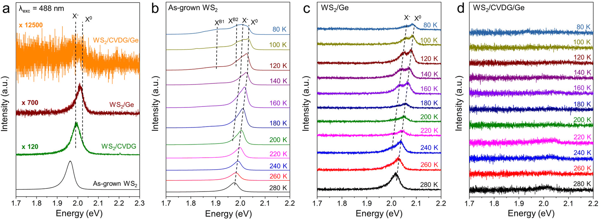 | ||
| Fig. 3 Comparative PL spectra of as-grown WS2, and annealed WS2/Ge and WS2/CVDG/Ge heterostructures obtained at both room temperature and reduced temperatures, down to 80 K. (a) A comparison of room-temperature PL of as-grown monolayer WS2, WS2/CVDG/SiO2/Si, WS2/Ge, and WS2/CVDG/Ge. WS2/CVDG/Ge heterostructures demonstrate the most prominent PL quenching effect, followed by WS2/Ge heterostructures. (b–d) Temperature-dependent PL spectra of as-grown WS2, WS2/Ge, and WS2/CVDG/Ge, respectively. The exciton species identified from the PL spectra are marked with black dashed lines in (a–c). | ||
Low-temperature PL spectroscopy is an effective method of identifying exciton species and optically probing defect states, because influences of thermal dissociation of bound excitons and the exciton–phonon interaction-induced PL linewidth broadening become less prominent at reduced temperatures, which allows different exciton species to be better resolved.47,48 Thus, to gain further insights into the PL properties of WS2/Ge heterostructures, we compared the temperature-dependent PL spectra of as-grown WS2, WS2/Ge, and WS2/CVDG/Ge in the temperature range of 80–280 K. Fig. 3b and c depict temperature-dependent PL spectra of as-grown WS2 monolayers and annealed WS2/Ge heterostructures, respectively. PL spectra of both samples show a gradual blue shift as the temperature decreases (∼70 meV shift from 280 K to 80 K), agreeing with the temperature-dependent band gap variation.49 In addition, by deconvoluting the PL spectra obtained at 80 K (Fig. S7†), it is possible to assign observed exciton species and track their evolution with temperature (black dashed lines in Fig. 3b and c). It is found that X0 dominates room-temperature PL spectra of both samples, while at lower temperature, the X− emission starts to emerge. This can be understood by the much smaller trion binding energy (∼30–50 meV) compared to the exciton binding energy (a few hundreds of meV), making X− easier to be thermally dissociated at a higher temperature.50 Moreover, multiple defect-bound excitons (XB1 and XB2) are present in as-grown WS2 at low temperatures, which are related to structural defects, such as sulfur vacancy-related defects.48 However, it is interesting to note that defect-related emissions are highly suppressed in WS2/Ge heterostructures. This implies that the defect-induced mid-gap states may be modified or passivated due to the electronic coupling between WS2 and Ge,51 which requires follow-up studies for further investigation. Finally, temperature-dependent PL measurement of WS2/CVDG/Ge was performed and the results are plotted in Fig. 3d. Similar to the room-temperature PL data in Fig. 3a, there is no observable enhancement/recovery of the PL signal at reduced temperatures, and the PL emission remains negligible at all of the measured temperatures, which again indicates the effective PL quenching caused by CVDG and the Ge substrate.
Mechanisms of photoluminescence quenching in the WS2/Ge system
DFT calculations were carried out to study the mechanisms of PL quenching in WS2/Ge from a theoretical perspective. DFT-PBE19 calculations, including vdW correction DFT-D2,20 were first performed on the bulk WS2 system to obtain the distance between WS2 monolayers; it is found that the distance between sulfur atoms in adjacent layers of WS2 is 3.10 Å (see Fig. 4a). Next, the distance between monolayer WS2 and the Ge(100) slab was calculated, and the optimized structure of WS2/Ge(100) is shown in Fig. 4b (side view) and Fig. 4c (top view). It is found that the separation of WS2 and Ge(100) is 2.50 Å (see Fig. 4b) and, therefore, the vdW interaction in WS2/Ge(100) is stronger than in bulk WS2. It is also well known that the band structure of WS2-type TMDs is very sensitive to the vdW interaction. For example, when the layer number is increased from monolayer to multilayer, TMDs become indirect band gap materials, with the direct band gap transition at the Brillouin zone K-point almost unchanged, but less accessible,3,52 which leads to a severely quenched PL in multilayer TMDs when compared to that of monolayers. A similar case with germanene, a 2D form of Ge, also revealed a reduction in the distance between interacting germanene and WS2 layers.53 Thus, it is possible that the enhanced interfacial interaction in WS2/Ge(100) can result in our experimentally observed PL quenching phenomenon. To verify this, we investigated the interfacial interaction and electronic behavior in the WS2/Ge(100) heterostructure. Note that a band gap correction approach is necessary through hybrid functionals as expressed in the HSE06 approach.21 First, the band gap was calculated for monolayer WS2 and bulk Ge, obtaining band gap values of 2.05 eV and 0.68 eV, respectively (Fig. 5a and b). It is worth mentioning that for monolayer WS2, the electronic single particle band gap was calculated (no excitonic effects were included). On the other hand, the calculated band gap value for bulk Ge agrees very well with previous experimental and calculated values (0.66 eV).54,55 For the WS2/Ge(100) heterostructure, by calculating the contribution of WS2 in the density of states (DOS) of WS2/Ge(100), it is found that the band gap of WS2 in WS2/Ge(100) is much reduced to 0.13 eV with multiple additional energy levels exhibited within the WS2 band gap (∼2 eV) due to the vdW interaction with the Ge surface, which makes the WS2 band gap less accessible and is likely responsible for the PL quenching. In addition, the adsorption energy (per unit surface area) was calculated by using the following relationship: Ead = EWS2 + EGe − EWS2/Ge where EWS2, EGe, and EWS2/Ge are the total energies for the WS2, Ge, and vdW WS2/Ge(100) system, respectively. The adsorption energy for the WS2/Ge(100) system was found to be 21.3 meV Å−2, which in combination with the small distance (2.50 Å) between WS2 and Ge(100) indicates that PL quenching is expected to occur, similar to the case of WS2 on sapphire.56 The case of hydrogenated Ge(100) [H-Ge(100), using a supercell with the same dimensions as WS2/Ge(100)] was also investigated by adding 32 H atoms at the open Ge sites on the top and bottom surfaces of Ge(100). For WS2/H-Ge(100), the distance between the topmost S atom in WS2 and the topmost H atom in H-Ge(100) is 2.22 Å (Fig. S8†) and Ead = 19.4 meV Å−2, which is similar to the previous case with no H-passivation in WS2/Ge(100). The slight distance reduction in the case of the WS2/H-Ge(100) system is similar to the effect seen in graphene/hydrogenated hexagonal boron nitride (H-hBN) heterostructures.57 Given the strong vdW interaction present in both the WS2/Ge(100) and WS2/H-Ge(100) systems, it is likely the PL quenching is caused by strong vdW interactions regardless of whether the Ge(100) substrate is H-passivated or not. | ||
| Fig. 4 DFT-calculated structures of bulk pristine WS2 and monolayer WS2 on a Ge(100) slab. (a) Structure of bulk WS2. The interlayer distance (the distance between sulfur atoms in adjacent layers) is calculated to be 3.10 Å. (b) Side view and (c) top view of monolayer WS2/Ge(100) heterostructures. The WS2-to-Ge distance is calculated to be 2.50 Å. | ||
 | ||
| Fig. 5 HSE-calculated DOS and band gaps of monolayer WS2, bulk Ge, and WS2/Ge(100) heterostructures. (a) Calculated DOS and band gap of monolayer WS2, indicating a band gap of 2.05 eV. (b) Calculated DOS and band gap of Ge, indicating a band gap of 0.68 eV. (c) Calculated WS2 contribution in the DOS of WS2/Ge(100) heterostructures. | ||
Conclusions
In this work, we prepared 2D/3D WS2/Ge(100) heterostructures and investigated in detail the PL properties of WS2/Ge and how they can be affected by post-transfer low-pressure Ar/H2 annealing. We found that WS2/Ge heterostructures exhibit a significant PL quenching when compared to as-grown WS2 monolayers, and post-transfer annealing can effectively improve the WS2/Ge interface quality and enhance the PL signal uniformity. Moreover, the temperature-dependent PL response of WS2/Ge was further studied and compared with those of as-grown WS2 and WS2/CVDG/Ge heterostructures. It is observed that WS2/Ge heterostructures exhibit consistent PL quenching effects from room temperature down to 80 K, and the defect-related emissions of WS2 are highly suppressed, possibly due to the modification or passivation of defect-induced mid-gap states. In addition, the PL signals of WS2/CVDG/Ge heterostructures are highly quenched and hardly distinguishable from the background noise. DFT calculations were performed to understand the mechanism of PL quenching in WS2/Ge(100). It is found that the vdW interactions at the WS2/Ge interface is stronger than in the bilayer or bulk of WS2, which leads to large modifications within the band gap of WS2. In all, this work demonstrates important roles of post-transfer treatment and substrate vdW interactions in the optical properties of TMDs/Ge heterostructures, paving the way for designing high-performance optoelectronic devices based on 2D/3D TMD/Ge heterostructures by interface engineering.Methods
Synthesis and transfer of monolayer WS2
For the synthesis of monolayer WS2, mixed WO3/NaBr powders are loaded in a porcelain boat, and a piece of clean SiO2 (300 nm)/Si substrate is placed on the top of the boat. Another porcelain boat with sulfur powders is placed upstream. During the synthesis, the furnace and S powder are heated up separately to 825 °C and 220 °C, respectively, and held for 10 min. Argon is used as a carrier gas throughout the process. For transferring WS2 monolayers to fabricate WS2/Ge heterostructures, the as-grown monolayer WS2 on SiO2/Si is first spin-coated with a layer of CA (10 mg mL−1 of CA in acetone). Subsequently, CA-coated WS2 is placed in buffered oxide etch (BOE) solution at room temperature, so that the SiO2 layer is etched, releasing the CA/WS2 film. After etching, the free-floating sample is rinsed in deionized water and transferred to a clean Ge(100) substrate. Finally, the CA film is dissolved in acetone/isopropanol baths, leaving WS2 transferred on the Ge substrate.Synthesis and transfer of graphene
To synthesize graphene, a piece of copper foil is first placed in a quartz tube furnace, which is purged with Ar at 0.5 L m−1 and a 15% H2–Ar mixture at 0.3 L m−1. The furnace is then brought to 1000 °C and the Cu is annealed for 30 min. Afterwards, the Ar flow rate is increased to 0.8 L m−1 and CH4 is introduced at 15 sccm for 7 minutes. Then CH4 is turned off, the Ar flow rate is returned to 0.5 L m−1, and the furnace is allowed to cool naturally to room temperature. The transfer of graphene involves spin-coating graphene on Cu with poly(methyl methacrylate) (PMMA) A6. Afterwards, the Cu is etched away by floating the sample on commercial Cu etchant from Alfa Aesar. Once the Cu has been etched, the supported graphene sample is placed in three separate water baths. After the final water bath, the sample is placed on the desired substrate and allowed to dry on a hotplate at 50 °C. To remove the PMMA, the sample is placed in acetone for 2 minutes, then dipped in isopropanol for several seconds and blow dried with nitrogen gas.DFT methods
DFT calculations are performed to understand the experimental observations by using supercells consisting of a layer of WS2 on a Ge slab. The generalized gradient approximation (GGA) by Perdew, Burke, and Ernzerhof (PBE)19 is used to obtain the relaxed coordinates. The calculations are performed with a plane wave kinetic energy cutoff of 612 eV with the atomic coordinates relaxed until the forces become smaller than 0.01 eV Å−1 and a self-consistent field (scf) energy convergence of 10−6 eV is achieved. The WS2/Ge(100) system is constructed in an orthorhombic supercell with dimensions of a = b = 16.3 Å and c = 50 Å with a single layer of WS2 consisting of 30 W and 60 S atoms on a Ge layer consisting of 144 Ge atoms, and the bulk WS2 system is constructed as a hexagonal unit cell with dimensions of a = b = 3.186 Å and c = 12.26 Å consisting of 2 W and 4 S atoms.58 The DFT-D2 correction is applied to describe the van der Waals interaction between the WS2 layer and the Ge slab.20 The density of states (DOS) is calculated to determine the contribution of the WS2 layer in the WS2/Ge(100) system by applying the HSE06 correction21 to the electronic structure obtained using the PBE functional. In order to accurately describe the behavior of WS2/Ge(100) using HSE06, the screening parameter is tuned to μ = 0.13 to best reproduce both the pure WS2 (2.03 eV)59 and Ge (0.66 eV) experimental band gaps.Author contributions
T. Z., A. V. and D. Z. contributed equally to this work. T. Z., A. V., A. L. E., M. R. and M. T. conceived the idea and designed the experiments. T. Z., D. Z., Z. Y. and M. L. synthesized and transferred the WS2 monolayers. T. G. N. and H. L. synthesized and transferred graphene. T. Z., A. V., D. Z., Z. Y. and K. O. D. A. performed the optical characterization. D. Z. and Y. L. performed the AFM characterization and analysis. Z. D. W. and H. T. performed the DFT calculations. All authors discussed the results and participated in the preparation of this manuscript.Conflicts of interest
There are no conflicts to declare.Acknowledgements
This work was supported by Air Force Office of Scientific Research Grant Number FA9550-18-1-0283 and FA9550-21-1-0460. H. T. and Z. D. W. acknowledge the funding support from the USA National Science Foundation (award 2013640) and are grateful to the “Advanced Cyberinfrastructure Coordination Ecosystem: Services & Support” (ACCESS), which is supported by National Science Foundation grant number ACI-1548562 through proposal TG-DMR170008.References
- D. Lembke, S. Bertolazzi and A. Kis, Acc. Chem. Res., 2015, 48, 100–110 CrossRef CAS PubMed.
- M. Bernardi, M. Palummo and J. C. Grossman, Nano Lett., 2013, 13, 3664–3670 CrossRef CAS PubMed.
- K. F. Mak, C. Lee, J. Hone, J. Shan and T. F. Heinz, Phys. Rev. Lett., 2010, 105, 136805 CrossRef PubMed.
- D. Y. Qiu, F. H. da Jornada and S. G. Louie, Phys. Rev. Lett., 2013, 111, 216805 CrossRef PubMed.
- D. Jariwala, T. J. Marks and M. C. Hersam, Nat. Mater., 2017, 16, 170–181 CrossRef CAS PubMed.
- M. Hong, P. Yang, X. Zhou, S. Zhao, C. Xie, J. Shi, Z. Zhang, Q. Fu and Y. Zhang, Adv. Mater. Interfaces, 2018, 5, 1800641 CrossRef.
- D. Ruzmetov, K. Zhang, G. Stan, B. Kalanyan, G. R. Bhimanapati, S. M. Eichfeld, R. A. Burke, P. B. Shah, T. P. O'Regan, F. J. Crowne, A. G. Birdwell, J. A. Robinson, A. V. Davydov and T. G. Ivanov, ACS Nano, 2016, 10, 3580–3588 CrossRef CAS PubMed.
- S. Krishnamoorthy, E. W. Lee, C. H. Lee, Y. Zhang, W. D. McCulloch, J. M. Johnson, J. Hwang, Y. Wu and S. Rajan, Appl. Phys. Lett., 2016, 109, 183505 CrossRef.
- S. Aftab, M. F. Khan, K. A. Min, G. Nazir, A. M. Afzal, G. Dastgeer, I. Akhtar, Y. Seo, S. Hong and J. Eom, Nanotechnology, 2018, 29, 045201 CrossRef PubMed.
- D. Sarkar, X. Xie, W. Liu, W. Cao, J. Kang, Y. Gong, S. Kraemer, P. M. Ajayan and K. Banerjee, Nature, 2015, 526, 91–95 CrossRef CAS PubMed.
- M. L. Tsai, S. H. Su, J. K. Chang, D. S. Tsai, C. H. Chen, C. I. Wu, L. J. Li, L. J. Chen and J. H. He, ACS Nano, 2014, 8, 8317–8322 CrossRef CAS PubMed.
- T. Akama, W. Okita, R. Nagai, C. Li, T. Kaneko and T. Kato, Sci. Rep., 2017, 7, 11967 CrossRef PubMed.
- D. Wu, J. Guo, C. Wang, X. Ren, Y. Chen, P. Lin, L. Zeng, Z. Shi, X. J. Li, C. X. Shan and J. Jie, ACS Nano, 2021, 15, 10119–10129 CrossRef CAS PubMed.
- W. Chen, R. Liang, S. Zhang, Y. Liu, W. Cheng, C. Sun and J. Xu, Nano Res., 2019, 13, 127–132 CrossRef.
- H. Wang, C. Zhang, W. Chan, S. Tiwari and F. Rana, Nat. Commun., 2015, 6, 8831 CrossRef CAS PubMed.
- O. Lopez-Sanchez, D. Lembke, M. Kayci, A. Radenovic and A. Kis, Nat. Nanotechnol., 2013, 8, 497–501 CrossRef CAS PubMed.
- W. Hu, H. Cong, W. Huang, Y. Huang, L. Chen, A. Pan and C. Xue, Light: Sci. Appl., 2019, 8, 106 CrossRef PubMed.
- L. Tang, S. E. Kocabas, S. Latif, A. K. Okyay, D.-S. Ly-Gagnon, K. C. Saraswat and D. A. B. Miller, Nat. Photonics, 2008, 2, 226–229 CrossRef CAS.
- J. P. Perdew, K. Burke and M. Ernzerhof, Phys. Rev. Lett., 1996, 77, 3865–3868 CrossRef CAS PubMed.
- S. Grimme, J. Antony, S. Ehrlich and H. Krieg, J. Chem. Phys., 2010, 132, 154104 CrossRef PubMed.
- J. Heyd, G. E. Scuseria and M. Ernzerhof, J. Chem. Phys., 2003, 118, 8207–8215 CrossRef CAS.
- F. Zhang, Y. Lu, D. S. Schulman, T. Zhang, K. Fujisawa, Z. Lin, Y. Lei, A. L. Elias, S. Das, S. B. Sinnott and M. Terrones, Sci. Adv., 2019, 5, eaav5003 CrossRef CAS PubMed.
- N. Higashitarumizu, H. Kawamoto, C. J. Lee, B. H. Lin, F. H. Chu, I. Yonemori, T. Nishimura, K. Wakabayashi, W. H. Chang and K. Nagashio, Nat. Commun., 2020, 11, 2428 CrossRef CAS PubMed.
- T. Zhang, K. Fujisawa, T. Granzier-Nakajima, F. Zhang, Z. Lin, E. Kahn, N. Perea-López, A. L. Elías, Y.-T. Yeh and M. Terrones, ACS Appl. Nano Mater., 2019, 2, 5320–5328 CrossRef CAS.
- Q. Yue, J. Kang, Z. Z. Shao, X. A. Zhang, S. L. Chang, G. Wang, S. Q. Qin and J. B. Li, Phys. Lett. A, 2012, 376, 1166–1170 CrossRef CAS.
- M. Buscema, G. A. Steele, H. S. J. van der Zant and A. Castellanos-Gomez, Nano Res., 2014, 7, 561–571 CrossRef.
- S. Tongay, W. Fan, J. Kang, J. Park, U. Koldemir, J. Suh, D. S. Narang, K. Liu, J. Ji, J. Li, R. Sinclair and J. Wu, Nano Lett., 2014, 14, 3185–3190 CrossRef CAS PubMed.
- I. Gasparutti, S. H. Song, M. Neumann, X. Wei, K. Watanabe, T. Taniguchi and Y. H. Lee, ACS Appl. Mater. Interfaces, 2020, 12, 7701–7709 CrossRef CAS PubMed.
- M. R. Rosenberger, H. J. Chuang, K. M. McCreary, A. T. Hanbicki, S. V. Sivaram and B. T. Jonker, ACS Appl. Mater. Interfaces, 2018, 10, 10379–10387 CrossRef CAS PubMed.
- F. Wang, J. Wang, S. Guo, J. Zhang, Z. Hu and J. Chu, Sci. Rep., 2017, 7, 44712 CrossRef CAS PubMed.
- K. Wang, B. Huang, M. Tian, F. Ceballos, M. W. Lin, M. Mahjouri-Samani, A. Boulesbaa, A. A. Puretzky, C. M. Rouleau, M. Yoon, H. Zhao, K. Xiao, G. Duscher and D. B. Geohegan, ACS Nano, 2016, 10, 6612–6622 CrossRef CAS PubMed.
- Y. Liu, C. Liu, Z. Ma, G. Zheng, Y. Ma and Z. Sheng, Appl. Phys. Lett., 2020, 117, 233103 CrossRef CAS.
- H. Fang, C. Battaglia, C. Carraro, S. Nemsak, B. Ozdol, J. S. Kang, H. A. Bechtel, S. B. Desai, F. Kronast, A. A. Unal, G. Conti, C. Conlon, G. K. Palsson, M. C. Martin, A. M. Minor, C. S. Fadley, E. Yablonovitch, R. Maboudian and A. Javey, Proc. Natl. Acad. Sci. U. S. A., 2014, 111, 6198–6202 CrossRef CAS PubMed.
- X. Wang, W. Fan, Z. Fan, W. Dai, K. Zhu, S. Hong, Y. Sun, J. Wu and K. Liu, Nanoscale, 2018, 10, 3540–3546 RSC.
- Z. Liu, M. Amani, S. Najmaei, Q. Xu, X. Zou, W. Zhou, T. Yu, C. Qiu, A. G. Birdwell, F. J. Crowne, R. Vajtai, B. I. Yakobson, Z. Xia, M. Dubey, P. M. Ajayan and J. Lou, Nat. Commun., 2014, 5, 5246 CrossRef PubMed.
- F. Liu, W. Wu, Y. Bai, S. H. Chae, Q. Li, J. Wang, J. Hone and X. Y. Zhu, Science, 2020, 367, 903–906 CrossRef CAS PubMed.
- I. H. Malitson, J. Opt. Soc. Am., 1965, 55, 1205–1209 CrossRef CAS.
- D. E. Aspnes and A. A. Studna, Phys. Rev. B: Condens. Matter Mater. Phys., 1983, 27, 985–1009 CrossRef CAS.
- M. Buscema, G. A. Steele, H. S. J. van der Zant and A. Castellanos-Gomez, Nano Res., 2015, 7, 561–571 CrossRef.
- H. Nan, Z. Wang, W. Wang, Z. Liang, Y. Lu, Q. Chen, D. He, P. Tan, F. Miao, X. Wang, J. Wang and Z. Ni, ACS Nano, 2014, 8, 5738–5745 CrossRef CAS PubMed.
- C. Hou, J. Deng, J. Guan, Q. Yang, Z. Yu, Y. Lu, Z. Xu, Z. Yao and J. Zheng, Phys. Chem. Chem. Phys., 2021, 23, 24579–24588 RSC.
- K. F. Mak, K. He, C. Lee, G. H. Lee, J. Hone, T. F. Heinz and J. Shan, Nat. Mater., 2013, 12, 207–211 CrossRef CAS PubMed.
- C. E. Giusca, I. Rungger, V. Panchal, C. Melios, Z. Lin, Y. C. Lin, E. Kahn, A. L. Elias, J. A. Robinson, M. Terrones and O. Kazakova, ACS Nano, 2016, 10, 7840–7846 CrossRef CAS PubMed.
- Y. C. Lin, C. Y. Chang, R. K. Ghosh, J. Li, H. Zhu, R. Addou, B. Diaconescu, T. Ohta, X. Peng, N. Lu, M. J. Kim, J. T. Robinson, R. M. Wallace, T. S. Mayer, S. Datta, L. J. Li and J. A. Robinson, Nano Lett., 2014, 14, 6936–6941 CrossRef CAS PubMed.
- C. Lee, H. Yan, L. E. Brus, T. F. Heinz, J. Hone and S. Ryu, ACS Nano, 2010, 4, 2695–2700 CrossRef CAS PubMed.
- T. Zhang, K. Fujisawa, F. Zhang, M. Liu, M. C. Lucking, R. N. Gontijo, Y. Lei, H. Liu, K. Crust, T. Granzier-Nakajima, H. Terrones, A. L. Elias and M. Terrones, ACS Nano, 2020, 14, 4326–4335 CrossRef CAS PubMed.
- O. A. Ajayi, J. V. Ardelean, G. D. Shepard, J. Wang, A. Antony, T. Taniguchi, K. Watanabe, T. F. Heinz, S. Strauf, X. Y. Zhu and J. C. Hone, 2D Mater., 2017, 4, 031011 CrossRef.
- V. Carozo, Y. Wang, K. Fujisawa, B. R. Carvalho, A. McCreary, S. Feng, Z. Lin, C. Zhou, N. Perea-Lopez, A. L. Elias, B. Kabius, V. H. Crespi and M. Terrones, Sci. Adv., 2017, 3, e1602813 CrossRef PubMed.
- Y. P. Varshni, Physica, 1967, 34, 149–154 CrossRef CAS.
- J. Huang, T. B. Hoang and M. H. Mikkelsen, Sci. Rep., 2016, 6, 22414 CrossRef CAS PubMed.
- K. Zhang, B. M. Bersch, J. Joshi, R. Addou, C. R. Cormier, C. Zhang, K. Xu, N. C. Briggs, K. Wang, S. Subramanian, K. Cho, S. Fullerton-Shirey, R. M. Wallace, P. M. Vora and J. A. Robinson, Adv. Funct. Mater., 2018, 28, 1706950 CrossRef.
- A. Splendiani, L. Sun, Y. B. Zhang, T. S. Li, J. Kim, C. Y. Chim, G. Galli and F. Wang, Nano Lett., 2010, 10, 1271–1275 CrossRef CAS PubMed.
- S. Sattar, N. Singh and U. Schwingenschlögl, Phys. Rev. B, 2016, 94, 205415 CrossRef.
- A. M. Al-Sheikh and K. S. Hameed, Rafidain J. Sci., 2011, 22, 58–68 CrossRef.
- C. A. Klein, J. Appl. Phys., 1968, 39, 2029–2038 CrossRef CAS.
- H. G. Ji, M. Maruyama, A. S. Aji, S. Okada, K. Matsuda and H. Ago, Phys. Chem. Chem. Phys., 2018, 20, 29790–29797 RSC.
- Z. Liu, R. Z. Wang, L. M. Liu, W. M. Lau and H. Yan, Phys. Chem. Chem. Phys., 2015, 17, 11692–11699 RSC.
- J. Wang and G. P. Srivastava, Nanomaterials, 2021, 11, 534 CrossRef CAS PubMed.
- J. Gusakova, X. Wang, L. L. Shiau, A. Krivosheeva, V. Shaposhnikov, V. Borisenko, V. Gusakov and B. K. Tay, Phys. Status Solidi A, 2017, 214, 1700218 CrossRef.
Footnotes |
| † Electronic supplementary information (ESI) available: Additional characterization results of WS2/Ge by optical imaging, fluorescence imaging, Raman spectroscopy, and AFM. Annealing effects on the PL of 2D WS2/CVDG heterostructures. Fitting results for the low-temperature PL spectra of as-grown WS2 and WS2/Ge. DFT-calculated structure of WS2/H-Ge(100). See DOI: https://doi.org/10.1039/d3nr00961k |
| ‡ These authors contributed equally to the work. |
| This journal is © The Royal Society of Chemistry 2023 |