
 Open Access Article
 This Open Access Article is licensed under a
 Creative Commons Attribution 3.0 Unported Licence
Intrinsic giant magnetoresistance due to exchange-bias-type effects at the surface of single-crystalline NiS2 nanoflakes†
Roman
Hartmann
 a,
Michael
Högen
b,
Daphné
Lignon
a,
Anthony K. C.
Tan
b,
Mario
Amado
c,
Sami
El-Khatib
d,
Mehmet
Egilmez
d,
Bhaskar
Das
e,
Chris
Leighton
e,
Mete
Atatüre
b,
Elke
Scheer
a and
Angelo
Di Bernardo
*af
a,
Michael
Högen
b,
Daphné
Lignon
a,
Anthony K. C.
Tan
b,
Mario
Amado
c,
Sami
El-Khatib
d,
Mehmet
Egilmez
d,
Bhaskar
Das
e,
Chris
Leighton
e,
Mete
Atatüre
b,
Elke
Scheer
a and
Angelo
Di Bernardo
*af
aDepartment of Physics, University of Konstanz, Konstanz 78457, Germany. E-mail: angelo.dibernardo@uni-konstanz.de
bCavendish Laboratory, University of Cambridge, Cambridge CB3 0HE, UK
cNanotechnology Group, University of Salamanca, Salamanca 37008, Spain
dDepartment of Physics, American University of Sharjah, Sharjah 26666, United Arab Emirates
eDepartment of Chemical Engineering and Materials Science, University of Minnesota, Minneapolis, MN 55455, USA
fDipartimento di Fisica “E. R. Caianiello”, Università degli Studi di Salerno, 84084 Fisciano, SA, Italy
First published on 9th May 2023
Abstract
The coexistence of different properties in the same material often results in exciting physical effects. At low temperatures, the pyrite transition-metal disulphide NiS2 hosts both antiferromagnetic and weak ferromagnetic orders, along with surface metallicity dominating its electronic transport. The interplay between such a complex magnetic structure and surface-dominated conduction in NiS2, however, is still not understood. A possible reason for this limited understanding is that NiS2 has been available primarily in bulk single-crystal form, which makes it difficult to perform studies combining magnetometry and transport measurements with high spatial resolution. Here, NiS2 nanoflakes are produced via mechanical cleaving and exfoliation of NiS2 single crystals and their properties are studied on a local (micron-size) scale. Strongly field-asymmetric magnetotransport features are found at low temperatures, which resemble those of more complex magnetic thin film heterostructures. Using nitrogen vacancy magnetometry, these magnetotransport features are related to exchange-bias-type effects between ferromagnetic and antiferromagnetic regions forming near step edges at the nanoflake surface. Nanoflakes with bigger steps exhibit giant magnetoresistance, which suggests a strong influence of magnetic spin textures at the NiS2 surface on its electronic transport. These findings pave the way for the application of NiS2 nanoflakes in van der Waals heterostructures for low-temperature spintronics and superconducting spintronics.
1. Introduction
Pyrite transition-metal disulfides (p-TMDs) are an interesting family of compounds, which have been investigated since the end of the 1960s in bulk single-crystalline form.1–6 Several p-TMDs also have magnetic properties,4 like CoS2, NiS2, and related compounds obtained from them, for example via substitutional doping of Fe for Co (e.g., Fe1−xCoxS2, for x > 0.05; ref. 3 and 4) or of Se for S (e.g., NiS2−xSex for x < 1 or CoS2−xSex for x < 0.6; ref. 4 and 6). Amongst magnetic p-TMDs, NiS2 is of particular interest for several reasons. First, the magnetic ground state of NiS2 is not fully understood, although this would be important also to understand the properties of other p-TMDs obtained, for example, from NiS2via substitutional doping. Second, several studies suggest that NiS2 can host different types of magnetic orderings at low temperature (T). In this complex magnetic state, non-collinear magnetic spin textures may arise, which could find, for example, applications in spintronic devices operating at low T, also in combination with superconductors.Unlike other transition-metal disulfides (TMDs) that are layered and can be exfoliated down to the monolayer limit, p-TMDs like NiS2 feature strong covalent/ionic bonds between their crystallographic planes. As a result of these strong bonds, p-TMDs are not easy to exfoliate in the form of nanoflakes, i.e., as samples with size in one dimension (typically the thickness) within the nanoscale range, and sizes along the other two dimensions in the micrometre range. This is one reason why most studies on p-TMDs to date have been carried out on p-TMDs in bulk single-crystalline form, which makes it difficult to obtain quantitative information about local variations in their physical properties using a combination of local electronic transport and magnetometry measurements, with high spatial resolution.
In addition to the coexistence of different types of magnetic ordering at low T, NiS2, which is a Mott insulator in the bulk, also features a metallic behaviour at its surface in the same low-T regime. From this point of view, NiS2 is a p-TMD that would be interesting to study as single-crystalline nanoflakes, to gain a better understanding of the interplay between magnetic textures and electronic transport in this material at the nanoscale.
In terms of its magnetic properties, NiS2 hosts a Type-I antiferromagnetic (AF) phase with long-range ordering (LRO) and a Néel temperature (TN1) typically of ∼38 K.7–10 Above TN1, NiS2 is paramagnetic.8 In the Type-I AF phase, the spin lattice of NiS2 consists of four sublattices with a unit cell equivalent to the chemical cell, with each of the four spins forming an angle θ = 12° ± 4° with respect to the principal axis of the electric field gradient at the Ni sites.11,12 This Type-I AF ordering of NiS2 on its face-centred cubic (fcc) lattice is also known as a triple-Q structure because the ground state of this AF phase is triply degenerate due to the fcc lattice symmetry.13–15 The triple-Q structure also exists in other materials, like γ-FeMn,13 γ-MnNi14 and NpO2.15
As T is lowered below TN1, a Type-II LRO AF phase also appears in NiS2 with a Néel temperature TN2 of ∼30 K.7,10,16–18 Although Type-I and Type-II AF phases should be incompatible in the fcc lattice of NiS2, they coexist over a certain temperature range as the result of a first-order phase transition accompanied, it has been proposed, by a small but finite distortion of the fcc lattice.19,20 This lattice distortion has been suggested to lift the degeneracy of the two AF phases,17 leading to a change in θ for the Type-I AF phase.11 A canting in the spin direction towards the [100] axis due to the lattice distortion also induces weak ferromagnetic (WF) ordering8–11 with onset temperature TWF coinciding with TN2. The precise origins of this WF phase, however, remains a matter of debate.10,21
Even more interesting is the fact that the coexistence of AF and WF orderings in NiS2 also occurs along with an enhancement in its surface electrical conduction at low T. Several experiments based on photoemission spectroscopy22 and on magnetotransport measurements23–25 (the latter also with NiS2 polycrystalline samples25) have shown that the NiS2 surface is more conductive than the bulk. As T is decreased, electronic transport in NiS2 thus becomes effectively two-dimensional (2D), meaning that transport is completely shunted by the NiS2 surface. Evidence for this is also provided by the fact that the contribution of the surface metallic conduction to the overall sample conductance at low T increases as the NiS2 thickness is reduced.23,24 Measurements of the magnetic susceptibility χ also show an increase of the contribution of the WF phase to the total magnetic moment,8 when this is normalised to the sample volume, as the thickness of the NiS2 single crystals decreases. Although those magnetic results were not confirmed in recent studies,24 the combination of the above observations suggests the possibility of a correlation between the surface conduction and the WF ordering at low T in ultrathin NiS2 crystals.
To reach a better understanding of the physical properties of NiS2 at low T, and of the interplay between electronic transport and magnetic spin textures, here we study NiS2 in the form of nanoflakes. These nanoflakes allow us to investigate electronic transport properties in NiS2 using local electrical contacts to NiS2, which we pattern with electron-beam lithography (EBL). We also apply a magnetometry technique with high spatial resolution – diamond quantum magnetometry (DQM) with nitrogen vacancy (NV) centres – to probe any spatial variations in the magnetic spin texture of NiS2, which is essential to interpret the magnetotransport measurements that we carry out on the same nanoflakes. We note here that magnetotransport measurements on NiS2 single crystals have been reported, but only down to T ≈ 35 K.24 On our NiS2 nanoflakes, we instead study magnetotransport down to T ≈ 1.5 K, and hence also below TWF, where the interplay between magnetism and electronic transport could trigger unusual phenomena due to the coexistence of AF and WF phases with 2D surface conduction.
2. Results and discussion
We produce NiS2 nanoflakes using a technique we have recently developed, which allows for the production of nanoflakes of any covalently or ionically bonded material in single-crystalline form, via subsequent cleaving and mechanical exfoliation of the same crystals.In particular, the fabrication starts by cleaving a NiS2 single crystal with a ceramic ZrO2 blade to prevent contamination of the smaller pieces of crystal obtained during this process. The cleaving is carried out in a glovebox in inert (N2) atmosphere directly on a piece of strong adhesive tape so that the smaller NiS2 crystals obtained at the end of this step are on the tape ready to be exfoliated. The smaller crystal pieces are then broken into nanoflakes by mechanical exfoliation and transferred onto a SiO2 (300 nm)/Si substrate with pre-patterned Au/Ti markers used as reference to locate the nanoflakes (Fig. 1a). The substrates are then mapped with an optical microscope inside the glovebox to detect those flakes which are likely NiS2. This is done because several other flakes of different materials (also from residues present in the tape) can be found on the substrate after exfoliation. The composition of the identified NiS2 flakes is confirmed by energy-dispersive X-ray (EDX) analysis, which is usually done after the measurements to avoid contamination of the interface between the contact electrodes and the NiS2 surface, or oxidation of the NiS2 surface before device fabrication.
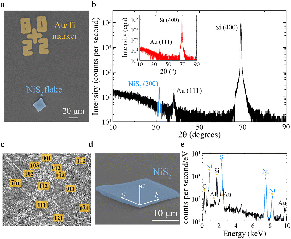 | ||
| Fig. 1 Structural characterisation and elemental composition analysis of the NiS2 nanoflakes. (a) Pseudo-colour scanning electron micrograph of a 420 nm-thick NiS2 nanoflake (light blue) on a SiO2(300 nm)/Si substrate with Au/Ti markers (yellow). (b) High-angle micro-XRD pattern of the NiS2 nanoflake (black curve) in (a) with NiS2 peaks in light blue. The red curve in the inset shows the micro-XRD pattern of substrate areas without nanoflakes. (c and d) Crystallographic axes orientation determined by electron back-scattered diffraction on a 650 nm-thick NiS2 nanoflake (c) and orientation of the cubic cell axes (white arrows) in (d). (e) Elemental composition analysis of the nanoflake in (d) based on energy-dispersive X-ray (EDX) spectroscopy. | ||
Unlike other NiS2 nanoflakes reported in the literature, which are prepared via chemical synthesis methods, mostly for water splitting applications,26,27 our NiS2 nanoflakes are single-crystalline because they are obtained from NiS2 single crystals, from which they must retain certain physical properties. The NiS2 nanoflakes reported in this study have a thickness ranging between ∼200 nm and 800 nm, which makes them about three orders of magnitude thinner than the thinnest NiS2 single-crystalline samples reported to date, which were produced by mechanical polishing.24 This reduced thickness of our NiS2 nanoflakes compared to single crystals should increase any surface-related contributions to charge transport, and in turn amplify any effects derived from the interplay between surface states and magnetic spin textures at low T.
Fig. 1a shows a typical NiS2 nanoflake that we obtain from a NiS2 single crystal (see ref. 24 for a description of the relevant single-crystal growth) on SiO2(300 nm)/Si with pre-patterned Au/Ti markers. In addition to being helpful for the location of the nanoflakes under an optical microscope, the markers are also used for alignment of the electron beam during the patterning of electrical contacts to the nanoflakes by EBL. The EBL patterning is then followed by magnetron sputtering of the electrode materials and removal of the EBL resist. We use sputtering of the contacts to get better coverage of the electrodes’ material along the nanoflake edges.
X-ray diffraction (XRD) measurements carried out with a micro-XRD (μ-XRD) setup show that our NiS2 nanoflakes always exfoliate along the same crystallographic axis, as they are all (200)-oriented (Fig. 1b). We can differentiate the diffraction peaks of the NiS2 nanoflakes from those generated by the Au/Ti markers and the substrate by performing μ-XRD measurements on substrate areas with markers but without nanoflakes (Fig. 1b; inset). The (200) orientation of our NiS2 nanoflakes is also confirmed by surface electron back-scattered diffraction (EBSD) measurements (Fig. 1c), which we carry out in a scanning electron microscope (SEM).
The EBSD data show that the NiS2 nanoflakes exfoliate with the a- and b-axis of the cubic unit cell oriented along the nanoflake edges (Fig. 1d). We also carried out EDX spectroscopy on all NiS2 nanoflakes investigated to confirm that their stoichiometry corresponds to the nominal stoichiometry of the NiS2 crystals from which the nanoflakes are obtained (Fig. 1e). The elemental analysis based on the EDX pattern of a NiS2 nanoflake reported in Fig. 1e, for example, confirms the stoichiometric 2![[thin space (1/6-em)]](https://www.rsc.org/images/entities/char_2009.gif) :1 ratio of S to Ni within experimental uncertainty.
:1 ratio of S to Ni within experimental uncertainty.
Using electrical contacts to the nanoflakes fabricated by EBL (Fig. 2a), we first characterise their electronic transport properties down to low T. The resistivity versus temperature, ρ(T), curves show different trends in the range 50 K < T < 150 K, depending on the material from which the electrical contacts to the NiS2 nanoflakes are made. When Au/Ti contacts are used, we sometimes measure non-linear current versus voltage curves, I(V), likely characteristic of poor transparency (i.e., high contact resistance) at the contact/nanoflake interface. With such Au/Ti contacts, ρ(T) monotonically increases from room T all the way down to low T (Fig. 2b). When Au/Pd contacts are used, however, for which linear I(V) curves are always measured, a decrease in ρ(T) occurs at 50 K < T < 150 K, before ρ(T) increases again for T < 50 K (Fig. 2c). We therefore relate the metallic behaviour shown in Fig. 2c for 50 K < T < 150 K to a better interface transparency (lower contact resistance) when we employ Au/Pd rather than Au/Ti contacts.
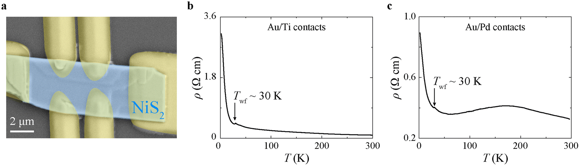 | ||
| Fig. 2 Electronic transport measurements on NiS2 nanoflakes. (a) Pseudo-colour scanning electron micrograph of a 550 nm-thick NiS2 nanoflake (light blue area) with Au/Pd electrical contacts (yellow areas) fabricated on top of the nanoflake. (b and c) Resistivity versus temperature, ρ(T), curves measured for a 380 nm-thick NiS2 nanoflake with Au/Ti contacts (b) and for a 400 nm-thick NiS2 nanoflake with Au/Pd contacts (c). | ||
The better interface transparency obtained with a Pd wetting layer may well be due to the larger molar enthalpy of formation of TiS2 (from −400 to −600 kJ mol−1; ref. 28) and other Ti sulfides, compared to that of PdS and other Pd sulfides (from −70 to −96 kJ mol−1; ref. 29). This likely favors interfacial metal/sulfide reactions (forming poorly-conducting TiS2, for example) when Au/Ti contacts are deposited, but not in the Au/Pd case. The transport data reported in the remaining part of this manuscript are thus collected on NiS2 nanoflakes with Au/Pd contacts, unless otherwise specified.
In a recent study,24 it has been shown that ρ(T) for NiS2 single crystals can change significantly depending on the surface preparation and thickness. For NiS2 single crystals that are thinned by mechanical polishing, for example, an enhancement in surface conduction is observed, which results in a flattening of ρ(T) at T < 150 K.24 Although our NiS2 nanoflakes are thinner by almost a factor of 103 than the thinnest NiS2 single crystals obtained by mechanical polishing in ref. 24, the ρ(T) curves that we measure (Fig. 2b and c) show similar trends to those reported for NiS2 single crystals without surface polishing,30,31 with a typical kink in ρ(T) around TWF. Nonetheless, the ρ(T) that we measure at low T (Fig. 2b and c) is smaller than that reported in ref. 24, consistent, significantly, with an increase in the contribution of surface metallic states to the electronic conduction in our ultrathin NiS2 nanoflakes.
To study the effect of magnetic spin textures in NiS2 on the electronic transport, we also carried out magnetotransport measurements on NiS2 nanoflakes. To the best of our knowledge, resistivity versus applied magnetic field, ρ(H), curves for NiS2 single crystals have only been reported for T > 35 K (i.e., above TWF),24 and measured with contact geometries much less local (i.e., on far bigger scales) than those of our nanoscale devices. Measurements on bulk crystals with wire-bonded contacts other than with local EBL-patterned contacts as in our study, for example, make it difficult to study electronic transport due to edge states, or to investigate the effect of few magnetic domains on electronic transport properties.
Here, we perform magnetotransport measurements as T is progressively lowered below TN1 and TWF to better understand the influence of both AF and WF order on electronic transport. The most striking magnetotransport features that we report are measured below TWF, i.e., at a T where the WF and AF orders coexist in NiS2. In this state, field-asymmetric features in the magnetoresistance (MR) are found (Fig. 3), meaning different values of ρ(H) for opposite H polarities. We define MR(H) = 100 × ((ρ(H) − ρ(0))/ρ(0)) here. A list of the devices for which we have performed MR measurements is reported in Table S1 of the ESI† together with some device parameters (e.g., direction of applied H, ρ at T = 300 K etc.). In Table S1,† we also identify each device with a number, which we also use to refer to a specific device in this manuscript.
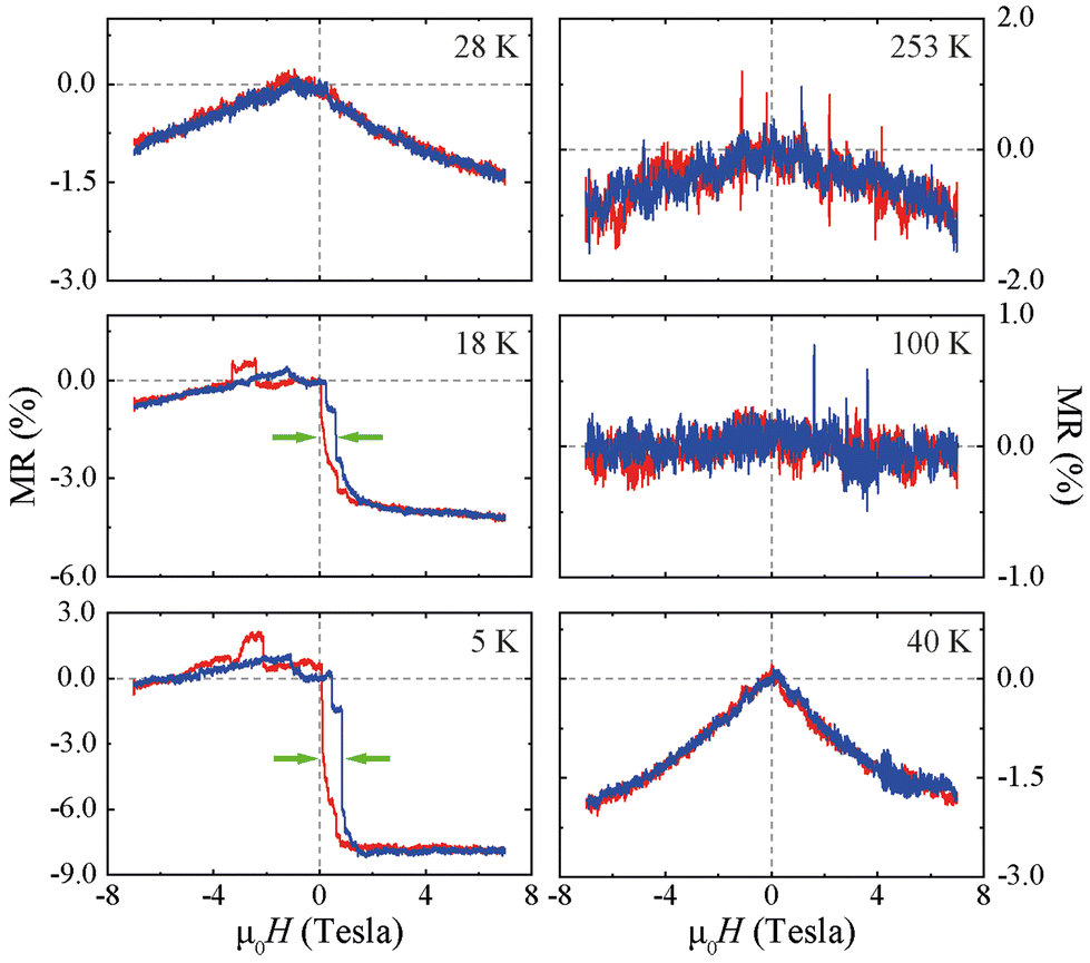 | ||
| Fig. 3 Magnetotransport measurements on NiS2 nanoflakes (device 1). Variation in magnetoresistance (MR) defined as MR(H) = 100 × (ρ(H) − ρ(H = 0))/ρ(H = 0) for a 380 nm-thick NiS2 nanoflake as a function of T with an in-plane applied H. Ascending and descending H sweeps are shown in blue and red, respectively, with the measurement T indicated in the top right corner of each panel. μ0 = 1.657 × 10⁻⁶ N A−2 is the vacuum permeability. Gray dashed lines indicate the MR measured at H = 0, whilst green arrows show the hysteretic MR loops that are shifted with respect to H = 0. | ||
Fig. 3 (where the applied H is in the plane of the flake) shows that for device 1 in the paramagnetic state of NiS2 (T > TN1), or in the Type-I AF state (TWF < T < TN1), we only measure field-symmetric MR(H) in agreement with other studies.24 As T is lowered below TWF, however, for all the devices investigated here, MR(H) assumes different values at the limits of the applied H range (i.e., [−7 Tesla, 7 Tesla]), meaning that it becomes strongly asymmetric with respect to H polarity. This asymmetric MR behaviour for opposite H directions at T < TWF occurs with both in-plane and out-of-plane H, and it is independent of the type of contacts used (Fig. 4). In addition, MR(H) also changes sign, going from negative to positive values in the intermediate range of the H that we apply (see, e.g., curves measured at 5 K and 18 K in Fig. 3 at negative H values between −3 T and 0 T). Lastly, we note that for some devices, at T < TWF, MR(H) also exhibited hysteretic loops that are shifted in H with respect to H = 0 (see Fig. 3 at 5 K and 18 K).
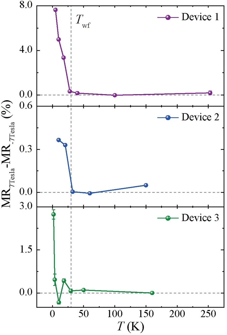 | ||
| Fig. 4 MR change at H = ±7 Tesla for different devices made on NiS2 nanoflakes with thicknesses of 380 nm (device 1; top panel), 790 nm (device 2; middle panel) and 400 nm (device 3; bottom panel). H is applied in plane for device 1 and out of plane for devices 2 and 3. | ||
The latter type of feature resembles the magnetotransport behaviour observed, for example, in spin valves based on thin film heterostructures with a ferromagnetic (F) layer exchange-biased by an AF layer exchange coupled to it. Critically, these asymmetric MR behaviours were observed in several devices not only for out-of-plane H (Fig. 4; devices 2 and 3), but also in-plane H (Fig. 4; device 1), ruling out that this MR behaviour is due to contamination of the MR signal by some anomalous Hall effect. A planar version of the latter might be envisioned also, but the behaviour of the MR asymmetry is essentially the same for out-of-plane and in-plane H (Fig. 4), making us confident that the observed asymmetry is not due to contamination of the typically field-even MR by field-odd Hall effects.
The MR curves for devices 2 and 3 are reported in Fig. S1 and S2 of the ESI file.† We observe that the MR(H) curves show a negative background above TWF when H is applied out of plane (device 1 in Fig. 3) and a positive background when H is within the plane (devices 2 and 3 in Fig. S1 and S2†).
The asymmetric and hysteretic MR(H) features shown above, and the fact that their onset T corresponds to TWF, also suggest that these features originate from the interplay between WF and AF orders, which coexist in NiS2 at T < TWF. One possible explanation for these MR features would be that the WF regions in NiS2 form adjacent to AF regions, resulting in exchange-coupled areas with different coupling strength that are sensitive to the applied H and strongly affect the local magnetotransport measurements. Exchange-bias-type effects at these WF/AF interfaces may then lead to asymmetric MR with hysteretic features like those that we report in Fig. 3.
To probe the above hypothesis and resolve the types of magnetic spin texture forming locally in NiS2, we also carried out DQM using commercially available diamond probes with a single NV centre at the apex of a diamond tip (Fig. 5f). The NV axis direction is defined by the angles (φNV and θNV), as shown by the schematic illustration of the DQM setup shown in Fig. 5f. The values of φNV, θNV and the distance of the NV centre from the sample surface (dNV) have been determined via independent measurements,32 as reported in the ESI.† The NV centre measures the projection of the stray field coming from the sample along the NV axis. The out-of-plane component of the magnetic field (Bz) at the sample is then reconstructed via the Fourier method.33
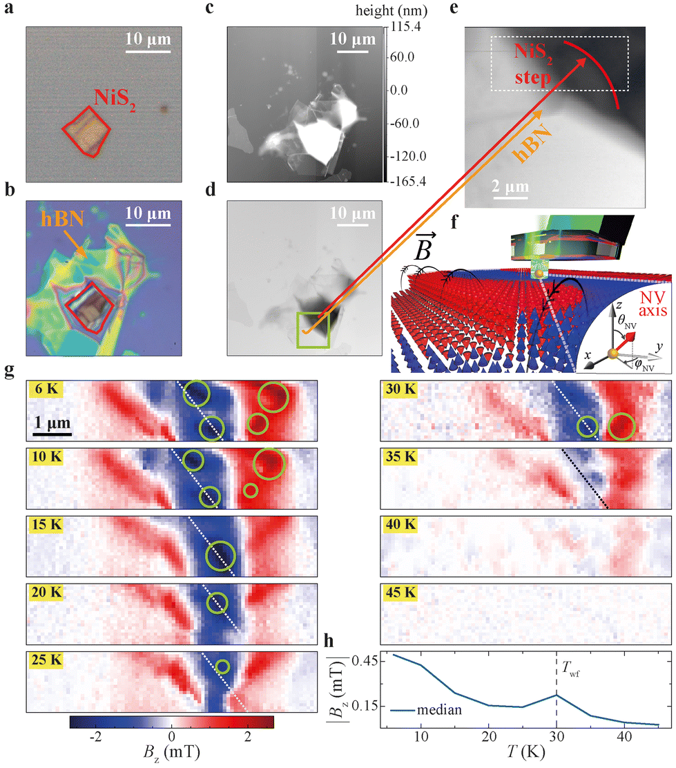 | ||
| Fig. 5 Diamond quantum magnetometry (DQM) measurements on NiS2 nanoflakes. (a–e) Optical microscope image of a NiS2 nanoflake before (a) and after capping with hBN (b) with atomic force microscopy image after capping in (c) and with inverted colour bar in (d). Panel (e) is a zoom in on the area in the green box of (d), with the white box highlighting where the DQM is done. (f) Schematic of the DQM setup. (g) Magnetic field Bz measured by DQM at different temperatures Ts (specified in the yellow boxes) on the NiS2 area corresponding to (e) showing regions with stroger Bz (green circles) close to a nanoflake step edge (dashed line). (h) Median value of Bzversus T over the nanoflake areas in (g). | ||
We note that, only for the DQM measurements, we used a hexagonal boron nitride (hBN) flake as capping layer to prevent the oxidation of the NiS2 nanoflakes (see ESI†). We performed DQM measurements as a function of T, whilst progressively reducing T below TN1 and TWF, to correlate possible changes in the magnetic signal probed by the NV spins with the onsets of the AF and WF orders. The results of the DQM measurements are shown in Fig. 5g for a representative NiS2 nanoflake. The measurement data show the absence of any significant Bz originating from the NiS2 nanoflakes at T > TN1, which agrees with the absence of any type of magnetic ordering in NiS2.
As T is reduced below TN1, however, an increase in the stray magnetic field signal probed by the NV spin is clearly observed. In particular, we detect regions of the nanoflakes that generate magnetic field with opposite direction (red and blue areas in Fig. 5g measured for T < TN1 ≈ 35 K). These regions likely correspond to areas with uncompensated moments on the NiS2 surface.
Characterisation of the surface topography of our NiS2 nanoflakes via atomic force microscopy indeed shows that they have a stepped surface (see, e.g., Fig. 5c–e). Such a stepped surface in the AF state of NiS2 could lead to the formation of areas with uncompensated magnetic moments,34 which would generate a non-null Bz for T < TN1. This Bz can also change polarity when moving from one terrace to another depending on the step height, which is consistent with the DQM data in Fig. 5g.
As T is reduced below TWF, we then detect additional regions with stronger Bz, which we associate with the WF order in NiS2, since they appear around TWF ∼ 30 K. The increase in Bz below TWF is also shown in Fig. 5h, where we report the median absolute value of Bz originating from the sample as a function of T. Our DQM data in Fig. 5h confirm that areas with stronger Bz (green circles in Fig. 5g), which we ascribe to the WF phase, emerge in proximity to AF regions with uncompensated moments that we resolve at the NiS2 surface at TWF < T < TN1. Since exchange coupling is known to arise at the interface between F regions and AF regions with uncompensated moments,35,36 exchange bias effects can account for the exchange-bias-like MR features observed at temperatures where AF and WF coexist (Fig. 3 and 4).
We also note that the regions with Bz that we associate with the WF phase are mostly localised near step edges on the NiS2 nanoflakes (see the dashed line in Fig. 5g), where the formation of AF areas with uncompensated moments is more likely. It is therefore reasonable to assume that near step edges the concentration of non-collinear magnetic textures and exchanged-bias regions increases. This means that nanoflakes with steeper edges should exhibit more asymmetric MR features and larger MR ratios than those we measure for NiS2 nanoflakes with a mostly flat surface (Fig. 3). To verify this, we selected NiS2 nanoflakes with higher steps and wider terraces and measured their MR(H) using contacts made to opposite sides of the nanoflake, across a step edge.
The results of these magnetotransport measurements are reported in Fig. 6 and Fig. S3† for two different NiS2 nanoflakes. For both nanoflakes, we measure a significant increase of the MR(H), which reaches values as high as 1370% for one of these nanoflakes at the limits of the applied H range (at T ∼ 26.6 K in Fig. 6b). More strongly asymmetric behaviour in MR for positive and negative H, and more pronounced exchange-biased-like features than those shown in Fig. 3 are also measured.
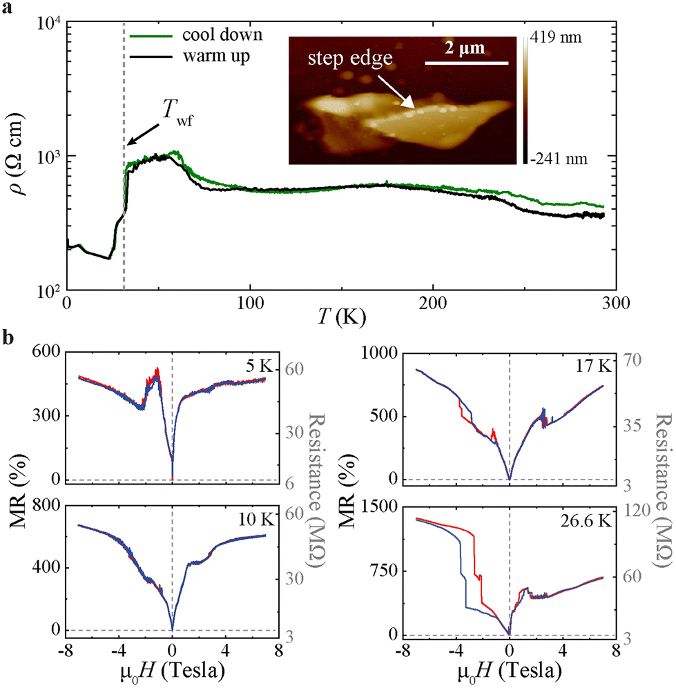 | ||
| Fig. 6 Magnetotransport measurements on a NiS2 nanoflake with high step edges (device 4). (a) Resistivity versus temperature, ρ(T), curves measured for a 280 nm-thick nanoflake. Atomic force microscopy image highlighting the step edges of the nanoflakes is shown as inset to panel (a). The dashed line in panel (a) marks TWF. (b) MR change as a function of the applied field H, MR(H), at a few representative temperatures (left axes) and corresponding resistance values (right axes) measured for the NiS2 nanoflake in (a). Ascending and discending H sweeps are shown in blue and red, respectively. | ||
The largest MR measured for the flake with a step edge in Fig. 6 at T ∼ 26.6 K occurs around the same T at which we also observe a peak-like feature in the Bz (mT) measured by DQM near the step edges of NiS2 nanoflakes (Fig. 5). The combination of these results suggests that the onset of the WF phase in NiS2 can indeed be the physical mechanism responsible for the large MR measured near step edges.
We note here that the expression ‘giant magnetoresistance’ has been originally introduced in the literature for spin valve devices based on thin film multilayers consisting of magnetic layers separated by non-magnetic ones.38 After its introduction, the same expression has been also used to describe changes in MR in magnetic thin film multilayers with exchange-bias effects at their interfaces.39,40 We therefore refer to the very large changes in MR that we measure in our NiS2 devices as giant magnetoresistance because the effects that we observe arise across interfaces between regions with different magnetic orders/spin textures, making them close to the effects observed for magnetic multilayer systems, for which the expression giant MR is routinely used.
For the two devices with step edges that we have measured (device 4 in Fig. 6 and device 5 in Fig. S3†), we find that the MR background is always positive, independent of the direction of H. For device 4, for example, where H is applied in plane, the MR background is positive at T > TWF. Similarly, for device 5 in Fig. S3,† the MR background remains positive, although H is applied out of plane. We believe that the positive MR background in devices with step edges is not a deterministic property, as the MR in such devices depends on a variety of factors, which makes its sign difficult to predict. First, the voltage signal that we measure in devices with step edges has both in-plane and an out-of-plane contributions from the bias current. Also, spin textures forming in these devices can exhibit complex patterns near step edges, as confirmed by the DQM data in Fig. 5, that can be randomly distributed with respect to the measurement electrodes every time a device with step edges is made. All these factors make it difficult to understand the origin and predict the sign of the MR background in such devices.
We further observe that the resistivity ρ(T) measured with the configuration of the electrical contacts across step edges shown in Fig. 6a and S3† takes on much larger values compared to those measured on nanoflakes with a flat surface (Fig. 3), but still in line with the ρ values reported in other studies of single crystals.24
The larger ρ measured on nanoflakes with higher steps (Fig. 6 and S3) is consistent with an increase in the current component that flows along the NiS2 out-of-plane direction, meaning across the bulk of the nanoflake, which is known to be less conductive than the surface. Also, the interplay between WF and AF phases is more strongly probed in this transport configuration, and it results in ρ(T) with sharp jumps and/or instabilities near the onset temperatures (TWF and TN1) of the two magnetic orders (Fig. 6 and S3). We also note that the MR curves show a host of very complex behaviours at low T, both in nanoflakes with and without step edges (Fig. 3a, 6 and S3†). Further studies, possibly with the support of micromagnetic simulations, will be needed to understand the complex T evolution of these MR features below TWF, parts of which we ascribe to the interplay between WF and AF phases in NiS2 nanoflakes. Also, magnetotransport measurements on bulk single crystals below TWF will have to be carried out to compare the low-T magnetotransport properties of bulk single crystals to those which we have measured for NiS2 nanoflakes.
3. Conclusions
In conclusion, we have fabricated NiS2 nanoflakes by exfoliating NiS2 single crystals, characterised their low-T magnetotransport properties, and correlated the magnetotransport data with the magnetic spin textures existing in the material by NV magnetometry. Nanoflakes with a flat surface show surface-dominated electronic transport at low T and field-asymmetric MR with hysteretic features that resemble those usually observed in more complex magnetic thin-film heterostructures. Based on our NV results, we correlate these MR features to exchange-bias-type effects originating at the interface between the WF regions and uncompensated moments of the Type-I AF regions at the NiS2 surface, which has a step-and-terrace topography. When nanoflakes with higher steps are tested, an extremely large increase in MR asymmetry and more pronounced exchange-bias-like features are measured. These results suggest that NiS2 nanoflakes host intrinsic exchange bias effects due to the coupling of surface regions with different types of magnetic orders at low T. As a result of the good surface metallicity of NiS2, exchange-coupled surface regions then have a strong effect on the magnetotransport properties of the NiS2 nanoflakes.One implication of our findings is that NiS2 nanoflakes could potentially be used as an alternative to more complex thin-film heterostructures for a variety of spintronic and device applications based on MR effects. The good metallicity of the flat nanoflakes, in combination with exchange-coupled spin textures, could also be exploited for the realisation of superconducting spintronic devices by coupling NiS2 nanoflakes to superconducting materials.37 In such systems, the magnetic spin textures at the metallic surface of NiS2 could be tested for the generation of long-range spin-triplet correlations.
Although the resistivity ρ of our NiS2 nanoflakes is three orders of magnitude lower than that of NiS2 single crystals,24 we also note that it increases at low T, which can in principle be a problem when coupling NiS2 nanoflakes to superconductors. Nonetheless, the absolute value of ρ at low T (∼1.0 Ω cm at T ∼ 4.2 K for nanoflakes with a flat surface; Fig. 2) is still lower than that of other TMDs like MoS2 (ref. 41 and 42) for which proximity-induced superconductivity has been observed.43,44 These results on other TMDs are therefore very encouraging with respect to coupling NiS2 to superconductors, which may result in an even stronger proximity effect due to the relatively low ρ of the NiS2 surface at low T.
Finally, we note that NiS2 nanoflakes can be picked up via the same dry-transfer technique used for other van der Waals (vdW) materials. This implies that the exchange-bias-type effects intrinsic to NiS2 nanoflakes could potentially be used for the realisation of novel exotic phases and quantum effects obtained by coupling NiS2 nanoflakes to other vdW materials.
Author contributions
A. D. B. conceived the project. R. H. exfoliated the NiS2 nanoflakes with some help from D. L. The nanoflakes were exfoliated from single crystals grown and characterised by C. L. and B. D., also with some support from S. E. K. and M. E. The fabrication of devices on NiS2 nanoflakes was done by R. H. and low-temperature magnetotransport measurements were carried out by R. H. and A. D. B, with some help from M. Am. The analysis of the magnetotransport data was done by R. H., E. S. and A. D. B. Diamond quantum magnetometry data were collected and analysed by M. H., A. K. C. T., and M. At. The manuscript was written by A. D. B. and R. H. with contributions to the text and comments on the results from all authors.Conflicts of interest
There are no conflicts to declare.Acknowledgements
R. H. and A. D. B. acknowledge funding from the Alexander von Humboldt Foundation in the framework of a Sofja Kovalevskaja grant and from the Zukunftskolleg at the University of Konstanz. A. D. B and E. S. also acknowledge funding from the Deutsche Forschungsgemeinschaft (DFG) through the SPP 2244 priority programme (grant No. 443404566). M. Am. acknowledges financial support from the Ministerio de Ciencia, Innovación y Universidades of Spain and FEDER (ERDF: European Regional Development Fund) under the research grant No. PID2019-106820RB-C21/22 and FEDER/Junta de Castilla y León grant No. SA121P20. Work performed at the University of Cambridge was supported by the Cambridge Nanoscale Sensing and Imaging Suite (CANSIS) as part of the Cambridge Henry Royce Institute under Engineering and Physical Sciences Research Council (EPSRC) grant No. EP/P024947/1 and from EPSRC QUES2T (EP/N015118/1). A. K. C. T. acknowledges funding from A*STAR through the National Science Scholarship. M. H. acknowledges funding from EPSRC NQIT (EP/M013243/1). S. E. K. acknowledges support from the American University of Sharjah under the FRG2020-M-S138 grant. Work at the University of Minnesota was supported by the US Department of Energy through the University of Minnesota Center for Quantum Materials under grant No. DE-SC0016371.References
- T. A. Bither, R. J. Bouchard, W. H. Cloud, P. C. Donohue and W. J. Siemons, Inorg. Chem., 1968, 7, 2208, DOI:10.1021/ic50069a008
.
- T. A. Bither, P. C. Donohue, W. H. Cloud, P. E. Bierstedt and H. S. Young, J. Solid State Chem., 1970, 1, 526, DOI:10.1016/0022-4596(70)90137-4
- H. S. Jarret, W. H. Cloud, R. J. Bouchard, S. R. Butler, C. G. Frederick and J. L. Gilson, Phys. Rev. Lett., 1968, 21, 617, DOI:10.1103/PhysRevLett.21.617
- S. Ogawa, J. Appl. Phys., 1979, 50, 2308, DOI:10.1063/1.327037
- G. Krill, M. F. Lapierre, C. Robert, F. Gautier, G. Czjzek, J. Fink and H. Schmidt, J. Phys. C: Solid State Phys., 1976, 9, 761, DOI:10.1088/0022-3719/9/5/016
- G. Krill, P. Panissod, M. Lahrichi and M. F. Lapierre-Ravet, J. Phys. C: Solid State Phys., 1979, 12, 4269, DOI:10.1088/0022-3719/12/20/021
- T. Miyadai, K. Takiyawa, H. Nagata, H. Ito, S. Miyahara and K. Hirakawa, J. Phys. Soc. Jpn., 1975, 38, 115, DOI:10.1143/JPSJ.38.115
- T. Thio, J. W. Bennet and T. R. Thurston, Phys. Rev. B: Condens. Matter Mater. Phys., 1995, 52, 3555, DOI:10.1103/PhysRevB.52.3555
- K. Kikuchi, T. Miyadai, H. Itoh and T. Fukui, J. Phys. Soc. Jpn., 1978, 45, 444, DOI:10.1143/JPSJ.45.444
- S. Yano, D. Louca, J. Yang, U. Chatterjee, D. E. Bugaris, D. Y. Chung, L. Peng, M. Grayson and M. G. Kanatzidis, Phys. Rev. B, 2016, 93, 024409, DOI:10.1103/PhysRevB.93.024409
- M. Matsuura, Y. Endoh, H. Hiraka, K. Yamada, A. S. Mishchenko, N. Nagaosa and I. V. Solovyev, Phys. Rev. B: Condens. Matter Mater. Phys., 2003, 68, 094409, DOI:10.1103/PhysRevB.68.094409
- Y. Nishihara, S. Ogawa and S. Waki, J. Phys. Soc. Jpn., 1975, 39, 63, DOI:10.1143/JPSJ.39.63
- Y. Endoh and Y. Ishikawa, J. Phys. Soc. Jpn., 1971, 30, 1614, DOI:10.1143/JPSJ.30.1614
- M. W. Long and O. Moze, J. Phys.: Condens. Matter, 1990, 2, 6013, DOI:10.1088/0953-8984/2/27/008
- M. W. Long, J. Phys.: Condens. Matter, 1989, 1, 2857, DOI:10.1088/0953-8984/1/17/008
- Y. Tokunaga, Y. Homma, S. Kambe, D. Aoki, H. Sakai, E. Yamamoto, A. Nakamura, Y. Shiokawa, R. E. Walstedt and H. Yasuoka, Phys. Rev. Lett., 2005, 94, 137209, DOI:10.1103/PhysRevLett.94.137209
- J. M. Hastings and L. M. Corliss, IBM J. Res. Dev., 1970, 14, 227, DOI:10.1147/rd.143.0227
- M. Matsuura, H. Hiraka, Y. Endoh, K. Hirota and K. Yamada, Appl. Phys. A, 2002, 74, s792, DOI:10.1007/s003390201585
- H. Nagata, H. Ito and T. Miyadai, J. Phys. Soc. Jpn., 1976, 41, 2133, DOI:10.1143/JPSJ.41.2133
- R. Shindou and N. Nagaosa, Phys. Rev. Lett., 2001, 87, 116801, DOI:10.1103/PhysRevLett.87.116801
- Y. Feng, R. Jaramillo, A. Banerjee, J. M. Honig and T. F. Rosenbaum, Phys. Rev. B: Condens. Matter Mater. Phys., 2011, 83, 035106, DOI:10.1103/PhysRevB.83.035106
- D. D. Sarma, S. R. Krishnakumar, E. Weschke, C. Schüßler-Langeheine, C. Mazumdar, L. Kilian, G. Kaindl, K. Mamiya, S. I. Fujimori, T. Fujimori and T. Miyadi, Phys. Rev. B: Condens. Matter Mater. Phys., 2003, 67, 155112, DOI:10.1103/PhysRevB.67.155112
- T. Thio and J. W. Bennet, Phys. Rev. B: Condens. Matter Mater. Phys., 1994, 50, 10574, DOI:10.1103/PhysRevB.50.10574
- S. El-Khatib, B. Voigt, B. Das, A. Stahl, W. Moore, M. Maiti and C. Leighton, Phys. Rev. Mater., 2021, 5, 115003, DOI:10.1103/PhysRevMaterials.5.115003
- K. D. M. Rao, T. Bhuvana, B. Radha, N. Kurra, N. S. Vidhzadhiraja and G. U. Kulkarni, J. Phys. Chem. C, 2011, 115, 10462, DOI:10.1021/jp201740q
- H. Ali, S. Ghosh and A. Mondal, Bull. Mater. Sci., 2021, 44, 230, DOI:10.1007/s12034-021-02519-x
- P. Yin, Z. Zhang, C. Zhou, Y. Sun, X. Han, C. Deng and L. Sun, Mater. Sci. Semicond. Process., 2014, 26, 404, DOI:10.1016/j.mssp.2014.04.037
- P. A. O′Hare and G. K. Johnson, J. Chem. Thermodyn., 1986, 18, 189, DOI:10.1016/0021-9614(86)90132-1
- A. Zubkov, T. Fujino, N. Sato and K. Yamada, J. Chem. Thermodyn., 1998, 30, 571, DOI:10.1006/jcht.1997.0328
- J. M. Honig and J. Spalek, Chem. Mater., 1998, 10, 2910, DOI:10.1021/cm9803509
- X. Yao, J. M. Honig, T. Hogan, C. Kannewurf and J. Spalek, Phys. Rev. B: Condens. Matter Mater. Phys., 1996, 54, 17469, DOI:10.1103/PhysRevB.54.17469
- L. Stefan, A. K. C. Tan, B. Vindolet, M. Högen, D. Thian, H. K. Tan, L. Rondin, H. S. Knowles, J. F. Roch, A. Soumyanarayanan and M. Atatüre, Phys. Rev. Appl., 2021, 16, 014054, DOI:10.1103/PhysRevApplied.16.014054
- E. A. Lima and B. P. Weiss, J. Geophys. Res.: Solid Earth, 2009, 114, B06102, DOI:10.1029/2008JB006006
- M. Charilaou and F. Hellman, J. Appl. Phys., 2015, 117, 083907, DOI:10.1063/1.4913594
- B. Henne, V. Ney, M. de Souza and A. Ney, Phys. Rev. B, 2016, 93, 144406, DOI:10.1103/PhysRevB.93.144406
- M. Gruyters and D. Schmitz, Phys. Rev. Lett., 2008, 100, 077205, DOI:10.1103/PhysRevLett.100.077205
- J. Linder and J. W. A. Robinson, Nat. Phys., 2015, 11, 307, DOI:10.1038/nphys3242
- M. N. Baibich, J. M. Broto, A. Fert, F. Nguyen Van Dau, F. Petroff, P. Etienne, G. Creuzet, A. Friederich and J. Chazelas, Phys. Rev. Lett., 1988, 61, 2472, DOI:10.1103/PhysRevLett.61.2472
- B. Dieny and J. Magn, Magn. Mater., 1994, 136, 335, DOI:10.1016/0304-8853(94)00356-4
- R. Coehoorn, Handb. Magn. Mater., 2003, 15, 1, DOI:10.1016/S1567-2719(03)15001-9
- Y. Fang, X. Hu, W. Zhao, J. Pan, D. Wang, K. Bu, Y. Mao, S. Chu, P. Liu, T. Zhai and F. Huang, J. Am. Chem. Soc., 2019, 141, 790, DOI:10.1021/jacs.8b12133
-
K. K. Kam, Electrical Properties of WSe2, WS2, MoSe2, MoS2, and Their Use as Photoanodes in a Semiconductor Liquid Junction Solar Cell, Thesis, Iowa State Univ., 1982. Thesis available at: https://archives.njit.edu/vol01/etd/2010s/2017/njit-etd2017-029/njit-etd2017-029.pdf. Search PubMed
- D. J. Trainer, B. Wang, F. Bobba, N. Samuelson, X. Xi, J. Zasadzinski, J. Nieminen, A. Bansil and M. Iavarone, ACS Nano, 2020, 14, 2718, DOI:10.1021/acsnano.9b07475
- M. Ramezani, I. C. Sampaio, K. Watanabe, T. Taniguchi, C. Schönenberger and A. Baumgartner, Nano Lett., 2021, 21, 5614, DOI:10.1021/acs.nanolett.1c00615
Footnote |
| † Electronic supplementary information (ESI) available. See DOI: https://doi.org/10.1039/d3nr00467h |
| This journal is © The Royal Society of Chemistry 2023 |