
 Open Access Article
 This Open Access Article is licensed under a
 Creative Commons Attribution 3.0 Unported Licence
Inkjet-printed h-BN memristors for hardware security†
Kaichen
Zhu
abc,
Giovanni
Vescio
b,
Sergio
González-Torres
 b,
Julià
López-Vidrier
b,
Juan Luis
Frieiro
b,
Sebastian
Pazos
a,
Xu
Jing
c,
Xu
Gao
c,
Sui-Dong
Wang
c,
Joaquín
Ascorbe-Muruzábal
d,
Juan A.
Ruiz-Fuentes
d,
Albert
Cirera
b,
Blas
Garrido
b and
Mario
Lanza
*a
b,
Julià
López-Vidrier
b,
Juan Luis
Frieiro
b,
Sebastian
Pazos
a,
Xu
Jing
c,
Xu
Gao
c,
Sui-Dong
Wang
c,
Joaquín
Ascorbe-Muruzábal
d,
Juan A.
Ruiz-Fuentes
d,
Albert
Cirera
b,
Blas
Garrido
b and
Mario
Lanza
*a
aMaterials Science and Engineering Program, Physical Science and Engineering Division, King Abdullah University of Science and Technology (KAUST), Thuwal 23955-6900, Saudi Arabia. E-mail: mario.lanza@kaust.edu.sa
bMIND, Department of Electronic and Biomedical Engineering, Universitat de Barcelona, Martí i Franquès 1, E-08028 Barcelona, Spain
cInstitute of Functional Nano & Soft Materials (FUNSOM), Collaborative Innovation Center of Suzhou Nano Science & Technology, Soochow University, 199 Ren-Ai Road, Suzhou 215123, P. R. China
dNadetech, Polígono Arbide, Calle V Nave 4, 31110 Noáin, Spain
First published on 26th May 2023
Abstract
Inkjet printing electronics is a growing market that reached 7.8 billion USD in 2020 and that is expected to grow to ∼23 billion USD by 2026, driven by applications like displays, photovoltaics, lighting, and radiofrequency identification. Incorporating two-dimensional (2D) materials into this technology could further enhance the properties of the existing devices and/or circuits, as well as enable the development of new concept applications. Along these lines, here we report an easy and cheap process to synthesize inks made of multilayer hexagonal boron nitride (h-BN)—an insulating 2D layered material—by the liquid-phase exfoliation method and use them to fabricate memristors. The devices exhibit multiple stochastic phenomena that are very attractive for use as entropy sources in electronic circuits for data encryption (physical unclonable functions [PUFs], true random number generators [TRNGs]), such as: (i) a very disperse initial resistance and dielectric breakdown voltage, (ii) volatile unipolar and non-volatile bipolar resistive switching (RS) with a high cycle-to-cycle variability of the state resistances, and (iii) random telegraph noise (RTN) current fluctuations. The clue for the observation of these stochastic phenomena resides on the unpredictable nature of the device structure derived from the inkjet printing process (i.e., thickness fluctuations, random flake orientations), which allows fabricating electronic devices with different electronic properties. The easy-to-make and cheap memristors here developed are ideal to encrypt the information produced by multiple types of objects and/or products, and the versatility of the inkjet printing method, which allows effortless deposition on any substrate, makes our devices especially attractive for flexible and wearable devices within the internet-of-things.
1. Introduction
2D layered materials exhibit outstanding physical, chemical, mechanical, electrical, optical, and magnetic properties that could be potentially exploited in a wide range of applications.1 Among them, the fabrication of solid-state microelectronic devices and circuits made of 2D materials has attracted much attention, as it may be a solution to produce advanced electronic devices and circuits beyond the complementary metal–oxide–semiconductor (CMOS) technology.2,3 However, most 2D material-based electronic devices consist of prototypes fabricated using methods that are not compatible with wafer-scale circuital technologies, such as mechanical exfoliation of small crystals.4 Chemical vapor deposition (CVD) is a scalable method to produce large-area 2D materials; however, the CVD method requires the use of high temperatures >850 °C, which impedes the direct growth of the 2D material on wafers containing CMOS circuits.5 This considerably complicates the fabrication process, as it makes necessary the use of a delicate process to transfer the 2D material to the target wafer.6 During this process, which is time-consuming, the CVD-grown 2D materials usually get contaminated and cracked.6–8Liquid phase exfoliation (LPE) is an inexpensive method to produce large amounts of few-nanometre-thick and few-micrometre-long sheets of different 2D layered materials, which consist of the use of an ultrasonic bath or microfluidization to exfoliate sheets from small bulk crystals—this is possible because the van der Waals forces that make the 2D planes attach to each other in the crystals are much weaker than the in-plane covalent bonding.1 Moreover, 2D materials synthesized by the LPE method can be deposited on any wafer at low temperature (by inkjet printing, screen printing, and spray, among others4) to pattern wires, electrodes, channels, and other complex devices with irregular shapes.9 This method has been used to fabricate a plethora of solid-state microelectronic devices, including transistors,10 photodetectors,11 capacitors,12 solar cells,13 and light emitting diodes14 (among others).
Memristors are emerging devices that are being commercialized as non-volatile memory devices (with a growing market size up to 621 million USD in 2021),15 and that have shown huge potential for data computation, encryption, and radio-frequency communication.16 Memristors made of 2D materials have shown interesting performance beyond flexibility and transparency, such as the coexistence of volatile and non-volatile switching, controllable potentiation and depression, ultra-low power consumption, and high thermal stability.17 However, few studies reported 2D-material-based memristors made by the inkjet printing method. Printed HfO2-based memristors exhibited non-volatile bipolar RS with ultra-low switching voltages of ±0.1 V.18 Inkjet-printed memristors made of 2D materials compared to those made of transition metal oxides (also done by inkjet printing) have shown a similar low operation voltage of 0.1–0.2 V, but with a large and tuneable on–off resistance ratio.19 However, in all these prototypes the dielectrics used (e.g. graphene oxide, MoS2, BP) are not very good electrical insulators, which results in low endurance (see ESI Tables 1–4†) and short retention times. In contrast, hexagonal boron nitride (h-BN) has a higher bandgap of ∼6 eV and has shown low leakage currents under polarization, which has been used to fabricate high-performance memristors using the CVD method.
In this work, we have synthesized printable h-BN inks from 2D crystals and afterward produced memristors with Ag/h-BN/Pt and Ag/h-BN/Ag structures (top-to-down) entirely by inkjet printing. The devices showed a high device-to-device variability of the initial resistance and forming voltage, as well as a high cycle-to-cycle variability of state resistances. These electrical features, combined with the cheap and scalable fabrication process, could enable the use of h-BN memristors as embedded hardware security primitives, such as PUFs to identify objects or entropy sources for data encryption circuits like TRNGs.
2. Results and discussion
Fig. 1a shows the photograph of the h-BN ink, which consists of a carboxy methyl cellulose solution containing h-BN nanoflakes; it shows a characteristic whitish colour. Fig. 1b shows the top-view scanning electron microscopy (SEM) image of an Ag/h-BN/Pt memristor as fabricated on a 300 nm SiO2/Si wafer. The h-BN nanoflakes form a continuous film with a surface roughness of 5.6 nm and a thickness of ∼250 nm, as demonstrated using top-view atomic force microscopy (AFM) (Fig. 1c) and cross-sectional SEM (Fig. 1d), respectively. Cross-sectional transmission electron microscopy (TEM) images of the Ag/h-BN/Pt devices reveal that the crystalline structure of the h-BN nanoflakes is excellent (see Fig. 1e–f and ESI Fig. 1†), and that their thickness fluctuates between 5 and 15 nm, which corresponds to 15 to 45 layers (see ESI Fig. 2†)—one monolayer of h-BN is 0.33 nm thick.20 Top-view TEM image of the flakes on a microperforated copper grid reveals that the average lateral length is ∼210 nm (see ESI Fig. 3†). The good crystal quality of the h-BN flakes was further confirmed using Raman spectroscopy (see ESI Fig. 4†).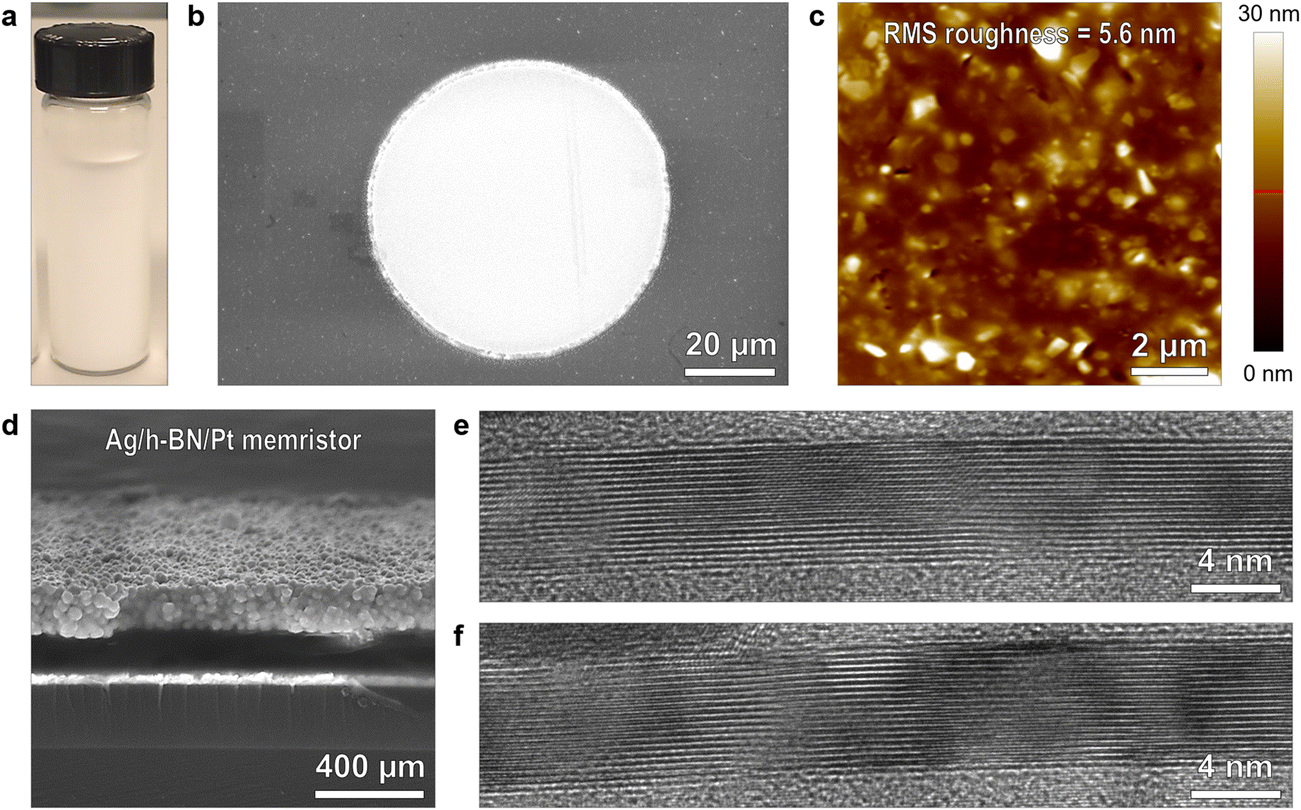 | ||
| Fig. 1 (a) Photograph of the h-BN ink. (b) Top-view SEM image of the inkjet-printed Ag/h-BN/Pt memristor. (c) Topographic AFM mapping of the inkjet-printed h-BN thin film. (d) Cross-sectional SEM image of the Ag/h-BN/Pt memristor. (e and f) Cross-sectional TEM images of h-BN nanoflakes with a perfect layered structure in the deposited thin film. | ||
We investigated the dielectric breakdown voltage and initial resistance of the 16 as-fabricated Au/h-BN/Pt memristors by applying sequences of ramped voltage stresses (RVS) and plotting the current versus voltage (I–V) curves. During the first RVS the Ag/h-BN/Pt memristors are initially in a high resistive state (HRS), and they transition to a low resistive state (LRS) sharply as the voltage increases. The sharp current increase and its high nonlinearity suggest that the switching mechanism is filamentary, most probably due to the drift of Ag+ ions from the top Ag electrode into the h-BN film when this is positively biased.21 The dielectric breakdown voltage and the initial resistance of the devices exhibit a very high device-to-device variability: from ∼0.4 to ∼16 V and from ∼107 to ∼1010 Ω, respectively (see Fig. 2a and b). This variability is related to the different structures of the devices, i.e., thickness fluctuations in the h-BN film and the formation of random junctions between the h-BN flakes, as well as different amounts of solvents and impurities present between the Pt and Ag electrodes. While this inherent device-to-device variability is detrimental for most memristive applications (memory, computation, and communication), it can be exploited to fabricate physical unclonable functions, i.e., circuits in which multiple devices are in an unpredictable state, and that can be used as a unique fingerprint within a system or to identify an object.16
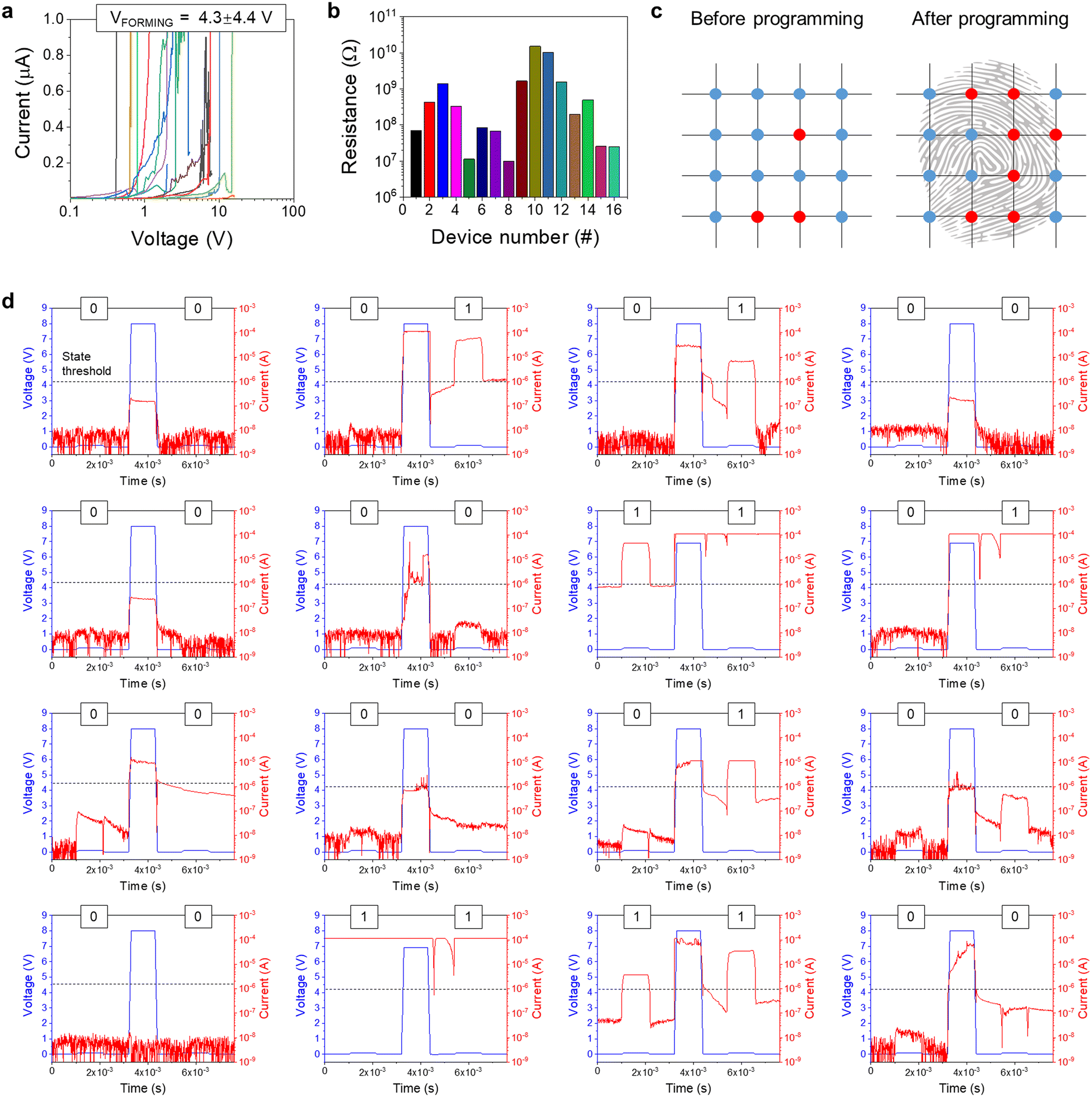 | ||
| Fig. 2 (a) I–V curves showing the forming process of 16 fresh Ag/h-BN/Pt memristors. (b) Column plot displaying the initial resistance of 16 fresh Ag/h-BN/Pt memristors with data extracted from (a). (c) Schematics showing the resistance mapping before and after the write pulse operation. The red dots represent memristors in the LRS (resistance <107 Ω), while the blue dots represent memristors in the HRS (resistance >107 Ω). (d) Read-write-read operation cycles of 16 fresh Ag/h-BN/Pt memristors under pulse mode with random forming processes. | ||
We analysed another 16 (different) devices by applying two read voltage pulses (height = 0.1 V; duration = 1 ms) with one write pulse between them (height = 8 V; duration = 1 ms), using an interval time between pulses of 1 ms (Fig. 2d). We observed that 13 out of 16 devices exhibit low currents <1 μA during the first read pulse (i.e., initial resistance >105 Ω), and the rest 3 devices were more conductive or shorted. By using 105 Ω as the threshold resistance to define two logic states (HRS = 0 and LRS = 1), it can be concluded that 18.75% of the devices analysed (3 out of 16) were initially in the LRS and the rest (13 out of 16, 81.25%) were in the HRS (see Fig. 2c, left panel).
Next, we analysed the resistance of this same group of devices during the second read pulse, i.e., after the application of the write pulse. As shown in Fig. 2d, 4 out of the 13 devices that were initially in the HRS switched to the LRS, and the rest (9 of 13) did not switched, creating a new pattern (Fig. 2c, right panel). Note that selecting a too-high write pulse height or duration would produce that all the devices switch to the LRS; and, conversely, selecting a too-low write pulse height or duration would produce that all devices remain in their initial state. Note that, first, predicting which devices will be in the HRS and which will be in the LRS (before and after the write pulse) is impossible because that is related to nanoscale variations of the composition of the devices; and second, the number of possible logic combinations for a group of 16 devices like the one in Fig. 2d is 216 = 65![[thin space (1/6-em)]](https://www.rsc.org/images/entities/char_2009.gif) 536. Hence, the high device-to-device variability of the initial resistance and forming voltage can be exploited to create unique patterns, and this could be used as a hardware security primitive to tag or identify objects or systems.
536. Hence, the high device-to-device variability of the initial resistance and forming voltage can be exploited to create unique patterns, and this could be used as a hardware security primitive to tag or identify objects or systems.
When positive and negative RVS are applied sequentially to the Ag/h-BN/Pt memristors, using a current limitation of 1 μA or lower during the positively increasing (i.e., forward) ramp, the devices exhibit volatile unipolar RS, also known as threshold type (Fig. 3a–d). In some cycles, the LRS need more time to relax back to the HRS. This switching behaviour is very reproducible in all the devices analysed. In some devices it can even reach a high switching endurance of up to 0.6 million cycles (see Fig. 3e), which is the highest endurance ever reported for any memristor fabricated by the LPE method with all the measured data plotted (see ESI Tables 1–4†). This behaviour could be exploited to fabricate electronic neurons for artificial neural networks.22,23 The statistical distribution of the resistance in the LRS and HRS show a clear separation of the 2 states (most cycles show RLRS/RHRS ∼ 10) with only limited cycle overlap (see Fig. 3f).
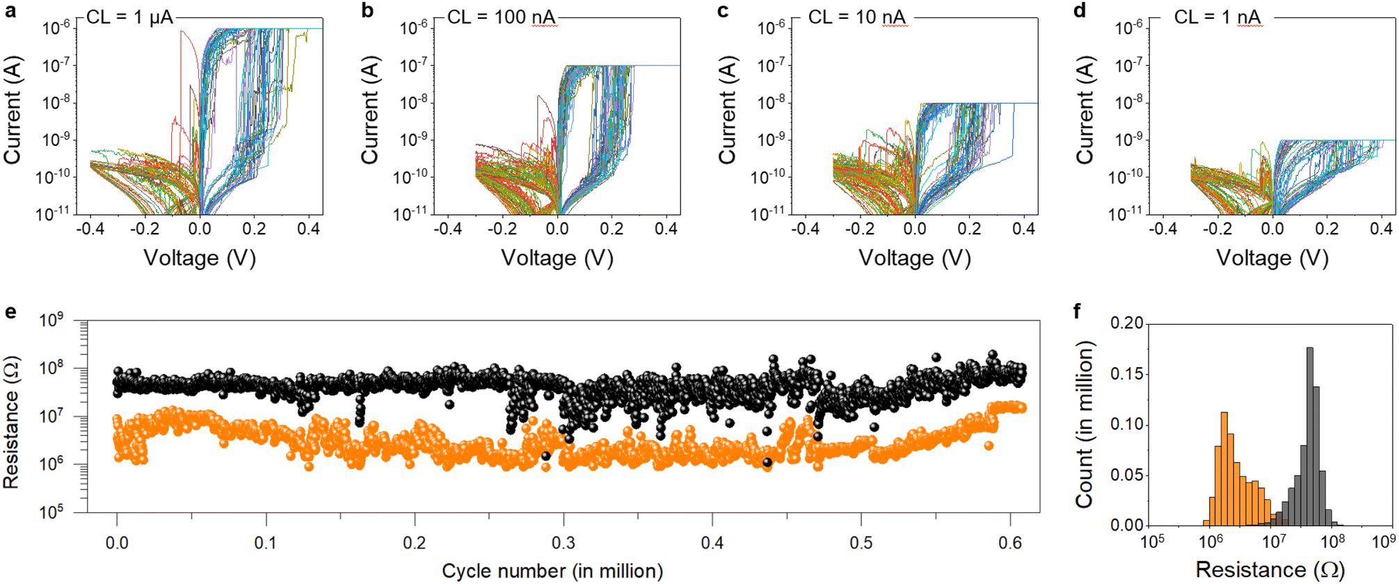 | ||
| Fig. 3 (a–d) I–V curves measured in the same Ag/h-BN/Pt memristor with different current limitations from 1 nA to 1 μA. (e) Column plot displaying the initial resistance of 16 fresh Ag/h-BN/Pt memristors with data extracted from (a). (e) Endurance test of Ag/h-BN/Pt under pulse operation. Write pulse 10 V 1 ms. Read pulse 0.1 V 1 ms. Time between pulses of 1 ms. (f) Statistical analysis of the resistance distribution of the HRS and LRS from (e). | ||
When the current limitation during the forward RVS is increased above 10 μA, the Ag/h-BN/Pt memristors exhibit correct non-volatile bipolar RS (see Fig. 4a). When a few RS cycles (<50) are measured via RVS the cycle-to-cycle variability of the state resistances is relatively low (Fig. 4b). However, when the devices are stressed using pulsed voltage stresses (PVS) the cycle-to-cycle variability of the state resistances remarkably increases, and it is remarkably higher in the HRS (Fig. 4d). The intrinsic cycle-to-cycle variability of RHRS could be used as an entropy source to generate random numbers sequentially by making a simple comparison with a threshold resistance value (RTH, below = 0 and above = 1). By setting RTH = 50 MΩ in Fig. 4d we obtained that, 656 of the cycles measured produce a 0 state, and 202 produce a 1 state. Predicting if the value of RHRS will be higher or lower than 107 Ω in one cycle is impossible, because that depends on the atomic structure after the previous reset event, which cannot be calculated or simulated even for the first cycle. By using a high current limitation of 1 mA one can generate a stable 2-state switching between the HRS and the LRS without overlapping of 2 orders of magnitude (see Fig. 4e).
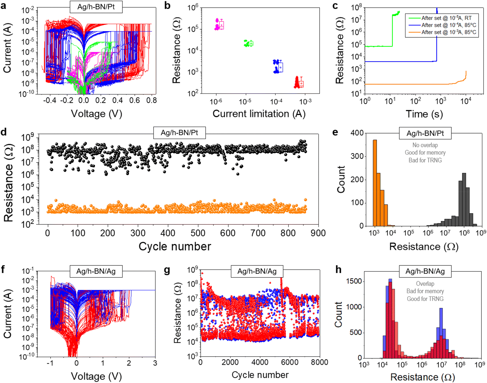 | ||
| Fig. 4 (a) I–V curves displaying 200 cycle bipolar RS in an Ag/h-BN/Pt memristor with current limitation from 1 μA to 0.5 mA. (b) Box plot of resistance vs. current limitation. (c) Retention test measured after set under different current limitations at a read voltage of 0.1 V. (d) Endurance test of an Ag/h-BN/Pt memristor under pulse operation with a current limitation of 1 mA. (e) Statistical analysis of the resistance distribution of the HRS and LRS in panel (d). (f) I–V curves displaying 150 cycle bipolar RS in an Ag/h-BN/Ag memristor with a current limitation of 1 mA. (g) Endurance test of Ag/h-BN/Ag under pulse operation with a current limitation of 1 mA, showing high stochasticity and unpredictable state after each event. (h) Statistical analysis of the resistance distribution of the HRS and LRS from (g), showing clear overlap. The clear overlap of the resistance distributions in the HRS and LRS shown in panel (h) confirms that these devices can be used as entropy sources for TRNGs. | ||
In these Ag/h-BN/Pt devices the LRS is not stable over long periods (i.e., the retention time is low), and most of them tend to self-switch back to the HRS (i.e., recover) after some time if the bias is reduced below 0.1 V (Fig. 4c). The higher the conductance in the LRS, the longer the recovery time (see Fig. 4c), but most of the devices end up recovering even when high current limitations up to 1 mA are used during the forward RVS. These observations further indicate that the RS mechanism is filamentary,21 and it is consistent with the highly-diffusive nature of the Ag+ ions penetrating into the LPE h-BN film when the devices are polarized.21 This self-recovery effect is positive for the functioning of the devices over time, as it warranties that the devices will not get stuck in LRS after some cycles—that is, the main failure mechanism of most memristors.24
Next, we maximized the randomness (i.e., variability) of RHRS after each cycle and further improve the recovery process (i.e., maximize the number of devices that recover and reduce the recovery time) by inkjet printing both top and bottom electrodes with Ag (on a SiO2/Si wafer). The fully-printed Ag/h-BN/Ag devices also exhibit stable non-volatile bipolar RS when applying sequences of RVS, but the cycle-to-cycle variability of the resistance in both states is much higher than in the Ag/h-BN/Pt devices (see Fig. 4f–h). The clear overlap of the resistance distributions in the HRS and LRS shown in Fig. 4h (something unwanted for memory applications but highly desired to build TRNG circuits) confirms that these devices can be used as entropy sources. The reason is that Ag+ ion injection can be triggered from both polarities since both the top and bottom electrodes are active metals. One genuine feature of the inkjet-printed Ag/h-BN/Ag memristors is that they never produce failure by getting stuck in one of the resistive states permanently. In the worst-case scenario the devices stop exhibiting stochasticity temporarily, and the high stochasticity recovers after some time (i.e., cycles), as shown in ESI Fig. 5.† All (i.e., 100%) of the devices that showed this phenomenon recovered, and the number of cycles in which the devices was stuck was <9%, which ensures good functioning. The fact that one device gets temporarily stuck at a given resistive state is not a problem at the application level, as this situation can be easily corrected in three different ways: (i) by applying more pulse trains or by increasing the pulse amplitude or duration;2 (ii) by redundancy, i.e., connecting more than one device so that at least one entropy source is available at the time;25 and (iii) by using a non-linear feedback shift register, as we did in our previous publication.26–29
Finally, we also find a good source of randomness when applying constant voltage stresses (CVS) to the Ag/h-BN/Pt memristors. In this case, the devices exhibit current fluctuations between two or more stable current levels at random times (see Fig. 5). Fig. 5a and b show a typical 2-state RTN signal, and Fig. 5c and d show a typical 3-state RTN signal. This type of behaviour is known as RTN,30,31 and it can also be exploited to fabricate TRGN circuits.26,32 It is known that two-state RTN is produced by charge trapping and de-trapping in a single defect, while up to four-state RTN is formed by the coupling between two defects.33 In memristive devices it is impossible to control if the RTN is two or three states, i.e., one applies a constant voltage and the two-state RTN signal may turn into three-state RTN (and vice versa) spontaneously. Controlling such a transition (for example, by changing the voltage applied) would imply to know if there is another defect in the device that would be activated at a specific voltage (i.e., energy level), but that cannot be known because it is related to the atomic structure of the device (the generation of defects in the device during fabrication is something considered totally random). In our h-BN memristors the current levels of the least conductive state in Fig. 5a (two-state) and Fig. 5c (three-state) overlap, meaning that the device can be used for TRNGs because a string of “0” and “1” can be randomly produced by detecting the transitions between the states using an AC-coupled amplifier.26–29 The advantage of stochastic RTN (Fig. 5) compared to stochastic resistive switching (Fig. 4f–h) is the lower energy consumption, because the currents never exceed the nanoampere regime (no filament is formed and disrupted in every transition). However, the ratio between the resistance states is much lower (∼2), which might complicate the hardware required to identify each logic state.
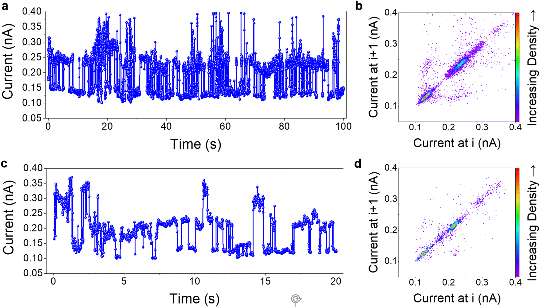 | ||
| Fig. 5 (a) RTN signal on an Ag/h-BN/Pt memristor among 2 states with a CVS of 0.1 V. (b) Time-lag (left axis) plus density dot (right axis) plot showing the capturing and releasing transition between 2 states of (a). (c) RTN signal on an Ag/h-BN/Pt memristor between 3 states with a CVS of 0.1 V, and the corresponding time-lag plus density dot plot (d). | ||
It should be highlighted that our inkjet-printed h-BN based memristors are very large (∼2800 μm2, see Fig. 1b), much larger than the normal device size used in commercial memristive memory (∼1 μm2). However, this is not a problem for the construction of TRNG and PUF circuits because the number of memristors needed is very small: TRNG circuits only use one memristor, from which they exploit the cycle-to-cycle variability of one switching parameter (VDB, VSET, tSET, RINI, an RHRS); and in PUFs only few devices are needed to generate a large number of possible combinations (i.e., 16 devices result in 65536 combinations). This device/these devices can be integrated right on the CMOS circuitry necessary to process the signal from the memristor, in which one of our TRNG designs occupies ∼24200 μm2 (using 180 nm CMOS technology).
3. Conclusion
In conclusion, we have fabricated h-BN memristors by inkjet printing technology. The devices exhibit a large device-to-device variability of the initial resistance and breakdown voltage, as well as volatile unipolar and non-volatile bipolar resistive switching with a very high cycle-to-cycle variability of state resistances; the devices also exhibit random telegraph noise. All these electronic behaviours are very stable, and hence they can be used as entropy sources in true random number generators and physical unclonable function circuits for data encryption. The reason why these stochastic phenomena are more accentuated in our devices (compared to other types of memristors) is the unpredictable morphology of the devices derived from the inkjet printing process (thickness fluctuations, orientations of the flakes). Our easy-to-make and cheap memristors could be an effective solution to encrypt the data produced by multiple objects and systems.4. Experimental section
h-BN ink formulation
An ink containing multilayer h-BN nanosheets has been formulated by liquid exfoliation of h-BN powder into a water-CMC (carboxy methyl cellulose) solvent. To achieve nanoflakes without clustering, CMC-Na was used to stabilize the flakes in solution due to the steric hindrance and the electrostatic repulsive forces from its charged groups (–CH2–COO−). The final ink contains h-BN flakes with thicknesses from 5 to 15 nm and lengths of ∼210 nm, and the concentration of flakes is ∼1 mg mL−1.Device fabrication
Ag/h-BN/Ag devices were constructed on standard glass substrates. First, the bottom Ag electrodes were printed using a Fujifilm Dimatix DMP inkjet printer equipped with a cartridge that offers a droplet volume of 10 pL. The Ag ink was purchased from Advanced Nano Product. Then, the h-BN ink was printed on the Ag bottom electrode using the same instrument. Finally, the top Ag electrode was also printed in the same way as the bottom electrode. All the inkjet-printed layers in the Ag/h-BN/Ag device were cured at 100 °C for 1 hour before the deposition of the next layer. Ag/h-BN/Pt devices were constructed on commercially available Pt/SiO2/Si substrates; Pt was deposited on a SiO2/Si wafer by electron beam evaporation. Then, we printed the h-BN film and the Ag electrodes on it and cured it at 150 °C for 1 hour. The devices had a circular shape with a diameter of 60 μm.Device characterization
The quality of the h-BN ink was characterized by scanning electron microscopy (Supra 55, Carl Zeiss), atomic force microscopy (Multimode V, Veeco), and transmission electron microscopy (JEOL JEM-2100 with a working voltage of 200 kV). The devices were characterized using a probe station (from M-150 from Cascade Microtech) connected with a semiconductor parameter analyser (Agilent B1500) and a temperature control stage (SP72-T2, ERS electronic GmbH). We tested the reproducibility and the cycle-to-cycle variability of switching by ramped voltage stresses (RVS) and pulsed voltage stresses (PVS). Constant voltage chronoamperometry was also performed to test the retention time at a given voltage at room temperature and 85 °C—this is the typical temperature at which reliability tests are normally performed.34 The stresses are always applied on the top electrode of the memristors, keeping the bottom electrode grounded.Author contributions
M. L. and K. Z. designed the project. K. Z., G. V., S. G. T., J. L. V., and J. L. F. fabricated and characterized the samples. S. P., X. J., X. G., S. D. W., J. A. M., J. A. R. F., A. C., and B. G. gave technical suggestions on the fabrication, characterization and/or simulations. K. Z. and M. L. wrote the manuscript, which was revised by all the authors.Conflicts of interest
There are no conflicts to declare.Acknowledgements
This work was supported by the National Key R&D Program of China (grant no. 2019YFE0124200, 2018YFE0100800), the National Natural Science Foundation of China (grant no. 61874075), and the Baseline funding scheme of the King Abdullah University of Science and Technology (KAUST). The authors also wish to acknowledge the financial support from MINECO (Spain) for Grant PID2019-105658RB-I00 (PRITES Project) and TED2021-129643B-I00 (FLEXRAM Project).References
- A. C. Ferrari, et al., Science and technology roadmap for graphene, related two-dimensional crystals, and hybrid systems, Nanoscale, 2015, 7, 4598 RSC.
- K. Zhu, et al., Hybrid 2D/CMOS microchips for memristive applications, Nature, 2023 DOI:10.1038/s41586-023-05973-1.
- K. Zhu, et al., The development of integrated circuits based on two-dimensional materials, Nat. Electron., 2021, 4, 775 CrossRef CAS.
- C. Backes, et al., Production and processing of graphene and related materials, 2D Mater., 2020, 7, 022001 CrossRef CAS.
- T. Chen, et al., Wafer-scale single-crystal hexagonal boron nitride monolayers on Cu (111), Nature, 2020, 579, 219 CrossRef CAS PubMed.
- J. D. Wood, et al., Annealing free, clean graphene transfer using alternative polymer scaffolds, Nanotechnology, 2015, 26, 5 CrossRef PubMed.
- Y. Shen, et al., Variability and yield in h-BN-based memristive circuits: The role of each type of defect, Adv. Mater., 2021, 33, 2103656 CrossRef CAS PubMed.
- G. Lupina, et al., Residual metallic contamination of transferred chemical vapor deposited graphene, ACS Nano, 2015, 9, 4776 CrossRef CAS PubMed.
- J. Li, et al., Inkjet printing of 2D layered materials, ChemPhysChem, 2014, 15, 3427 CrossRef CAS PubMed.
- T. Carey, et al., Fully inkjet-printed two-dimensional material field-effect heterojunctions for wearable and textile electronics, Nat. Commun., 2017, 8, 1202 CrossRef PubMed.
- R. Hossain, et al., Biocompatible, large-format, inkjet printed heterostructure MoS2-graphene photodetectors on conformable substrates, npj 2D Mater. Appl., 2017, 1, 28 CrossRef.
- R. Worsley, et al., All-2D material inkjet-printed capacitors: toward fully printed integrated circuits, ACS Nano, 2019, 13, 54 CrossRef CAS PubMed.
- B. Wilk, et al., Inkjet printing of quasi-2D perovskite layers with optimized drying protocol for efficient solar cells, Adv. Mater. Technol., 2022, 6, 2200606 CrossRef.
- G. Vescio, et al., 2D PEA2SnI4 inkjet-printed halide perovskite LEDs on rigid and flexible substrates, ACS Energy Lett., 2022, 7, 3653 CrossRef CAS PubMed.
- Emerging non-volatile memory [market analysis report]. Yole Development (2021); https://www.i-micronews.com/products/emerging-non-volatile-memory-2021/.
- M. Lanza, et al., Memristive technologies for data storage, computation, encryption, and radio-frequency communication, Science, 2022, 376, eabj9979 CrossRef CAS PubMed.
- M. Lanza, et al., Resistive switching crossbar arrays based on layered materials, Adv. Mater., 2023, 35, 2205402 CrossRef CAS PubMed.
- G. Vescio, et al., Low-power, high-Performance, non-volatile inkjet-printed HfO2-based resistive random access memory: From Device to Nanoscale Characterization, ACS Appl, Mater. Interfaces, 2019, 11, 23659 CrossRef CAS PubMed.
- A. A. Bessonov, et al., Layered memristive and memcapacitive switches for printable electronics, Nat. Mater., 2015, 14, 199 CrossRef CAS PubMed.
- C. Zhang, et al., Controllable co-segregation synthesis of wafer-scale hexagonal boron nitride thin films, Adv. Mater., 2014, 26, 1776 CrossRef CAS PubMed.
- Z. Wang, et al., Memristors with diffusive dynamics as synaptic emulators for neuromorphic computing, Nat. Mater., 2017, 16, 101 CrossRef CAS PubMed.
- Q. Duan, et al., Spiking neurons with spatiotemporal dynamics and gain modulation for monolithically integrated memristive neural networks, Nat. Commun., 2020, 11, 3399 CrossRef CAS PubMed.
- J. B. Roldan, et al., Spiking neural networks based on two-dimensional materials, npj 2D Mater. Appl., 2022, 6, 63 CrossRef.
- M. Lanza, et al., Standards for the characterization of endurance in resistive switching devices, ACS Nano, 2021, 15, 17214–17231 CrossRef CAS PubMed.
- H. Martin, G. D. Natale and L. Entrena, Towards a dependable true random number generator with self-repair capabilities, IEEE Trans. Circuits Syst., 2018, 65, 247–256 Search PubMed.
- C. Wen, et al., Advanced data encryption using two-dimensional materials, Adv. Mater., 2021, 33, 2100185 CrossRef CAS PubMed.
- S. Pazos, et al., High-temporal-resolution characterization reveals outstanding random telegraph noise and the origin of dielectric breakdown in h-BN memristors, Adv. Funct. Mater., 2023, 2213816 CrossRef.
- S. Pazos, et al., Hardware implementation of a true random number generator integrating a hexagonal boron nitride memristor with a commercial microcontroller, Nanoscale, 2023, 15, 2171–2180 RSC.
- X. Li, et al., Random telegraph noise in metal-oxide memristors for true random number generators: a materials study, Adv. Funct. Mater., 2021, 2102172 CrossRef CAS.
- N. Raghavan, et al., Microscopic origin of random telegraph noise fluctuations in aggressively scaled RRAM and its impact on read disturb variability, in IEEE International Reliability Physics Symposium (IRPS), 2013, 5E.3.1–5E.3.7 Search PubMed.
- H. Abunahla, et al., SecureMem: efficient flexible Pt/GO/Cu memristor for true random number generation, Flex. Print. Electron., 2021, 6, 035004 CrossRef CAS.
- F. M. Puglisi, et al., Random telegraph noise in resistive random access memories: compact modeling and advanced circuit design, IEEE Trans. Electron Devices, 2018, 65, 2964 CAS.
- T. Grasser, Noise in Nanoscale Semiconductor Devices, Springer Nature. 2020 ISBN 978-3-030-37499-0. DOI:10.1007/978-3-030-37500-3.
- M. Lanza, et al., Recommended methods to study resistive switching devices, Adv. Electron. Mater., 2018, 1800143 Search PubMed.
Footnote |
| † Electronic supplementary information (ESI) available. See DOI: https://doi.org/10.1039/d3nr00030c |
| This journal is © The Royal Society of Chemistry 2023 |