
 Open Access Article
 This Open Access Article is licensed under a
 Creative Commons Attribution 3.0 Unported Licence
Large area roll-to-roll printed semiconducting carbon nanotube thin films for flexible carbon-based electronics†
Jiaqi
Li
abc,
Min
Li
bc,
Zhaofeng
Chen
c,
Shuangshuang
Shao
bc,
Weibing
Gu
 bc,
Ying
Gu
abc,
Yuxiao
Fang
*bc and
Jianwen
Zhao
*bc
bc,
Ying
Gu
abc,
Yuxiao
Fang
*bc and
Jianwen
Zhao
*bc
aInstitute of Nano Science and Technology, University of Science and Technology of China, No. 166 Ren Ai Road, Suzhou Industrial Park, Suzhou, Jiangsu Province 215123, PR China
bSchool of Nano-Tech and Nano-Bionics, University of Science and Technology of China, No. 398 Ruoshui Road, Suzhou Industrial Park, Suzhou, Jiangsu Province 215123, PR China. E-mail: jwzhao2011@sinano.ac.cn; yxfang2021@sinano.ac.cn
cDivision of Nanodevices and Related Nanomaterials, Suzhou Institute of Nano-Tech and Nano-Bionics, Chinese Academy of Sciences, No. 398 Ruoshui Road, Suzhou Industrial Park, Suzhou, Jiangsu Province 215123, PR China
First published on 27th January 2023
Abstract
A universal roll-to-roll (R2R) printing approach was developed to construct large area (8 cm × 14 cm) semiconducting single-walled carbon nanotube (sc-SWCNT) thin films on flexible substrates (such as polyethylene terephthalate (PET), paper, and Al foils) at a printing speed of 8 m min−1 using highly concentrated sc-SWCNT inks and crosslinked poly-4-vinylphenol (c-PVP) as the adhesion layer. Bottom-gated and top-gated flexible printed p-type TFTs based on R2R printed sc-SWCNT thin films exhibited good electrical properties with a carrier mobility of ∼11.9 cm2 V−1 s−1, Ion/Ioff ratios of ∼106, small hysteresis, and a subthreshold swing (SS) of 70–80 mV dec−1 at low gate operating voltages (±1 V), and excellent mechanical flexibility. Furthermore, the flexible printed complementary metal oxide semiconductor (CMOS) inverters demonstrated rail-to-rail voltage output characteristics under an operating voltage as low as VDD = −0.2 V, a voltage gain of 10.8 at VDD = −0.8 V, and power consumption as low as 0.056 nW at VDD = −0.2 V. To the best of our knowledge, the electrical properties of the printed SWCNT TFTs (such as Ion/Ioff ratio, mobility, operating voltage, and mechanical flexibility) and printed CMOS inverters based on the R2R printed sc-SWCNT active layer in this work are excellent compared to those of R2R printed SWCNT TFTs reported in the literature. Consequently, the universal R2R printing method reported in this work could promote the development of fully printed low-cost, large-area, high-output, and flexible carbon-based electronics.
1. Introduction
In recent years, printed electronics1–3 and their applications have been intensively studied and achieved tremendous development,1,4 owing to new materials and the improvement of printing technology.5–8 The potential of this additive manufacturing technique for low-cost mass production, rapid prototyping of small series, and low-temperature fabrication on flexible substrates9,10 makes it an attractive alternative to conventional fabrication methods for electronics.11 It is known that the properties of channel materials determine the electrical properties of printed thin film transistors (TFTs).12 Solution-processable semiconductor materials in the forms of organic compounds,3,13–16 graphene,17–22 carbon nanotubes, and oxides23,24 have been developed to be compatible with current printing techniques.25–31 Among them, semiconducting single-walled carbon nanotubes (sc-SWCNTs) are a promising candidate for high-performance flexible printed electronics due to their high carrier mobility, excellent chemical stability, mechanical stability, and compatibility with solution-based printing processes. Printed TFTs based on sc-SWCNTs have attracted much attention in the past few decades and have proven to be the fundamental components of32–34 logic circuits, sensors,29,35–38 and displays.39–41 Various printing methods such as screen printing, inkjet printing, and transfer printing processes have been used to fabricate SWCNT-TFTs on flexible or rigid substrates, but there still needs to be a breakthrough to achieve industrial production.42 An important reason is the size and cost limitation of the current mainstream printing process.Roll-to-roll (R2R) printing technology is promising due to its high-output, large-area, and low-cost advantages.28,43,44 Furthermore, the final packaging of R2R-printed electronics into product devices is simple and convenient since only cutting and pasting processes are required.45–48 Although R2R printing has been used to construct SWCNT TFTs on polyethylene terephthalate (PET) rolls for different sensors,49–52 display active matrices, logic gates, circuits, etc.,44,53–55 the reported SWCNT TFTs exhibited poor electrical characteristics (such as low Ion/Ioff ratios, high operation voltage and low mobility) and unstable yield values owing to the lack of high-quality sc-SWCNT inks and thin films and unsuitable printable dielectric materials, which hinders the industrial production of R2R printing.48,50,51,56,57
In this work, we first reported an R2R ultra-fast (8 m min−1) printing of large-area (8 cm × 14 cm, theoretically infinite in length, which is limited by the R2R printing machine), high-quality sc-SWCNT thin films on different substrates (PET, Al, and paper) with a fast cure time (<5 s) and a low cure temperature (<150 °C) and without any solvent rinsing after optimizing the sorted sc-SWCNT ink concentrations and printing times. The as-prepared sc-SWCNT thin films can be directly used to fabricate top-gated and bottom-gated flexible TFTs and complementary metal oxide semiconductor (CMOS) inverters without any other post-treatment. The fabricated p-type TFT devices showed a high carrier mobility (∼11.9 cm2 V−1 s−1), high Ion/Ioff ratios (105–106), small hysteresis (40 mV), and small subthreshold swing (SS) (70–80 mV dec−1) with the gate voltage varying from −1 V to 1 V. Furthermore, the constructed flexible CMOS inverters exhibited good properties with rail-to-rail voltage output characteristics (even the operating voltage as low as VDD = −0.2 V), a voltage gain of 11 at VDD = −0.8 V, and power consumption as low as 0.056 nW at VDD = −0.2 V. Compared with other reports about R2R printed SWCNT electronics, our TFT devices and CMOS inverters exhibited excellent properties. The work demonstrates the potential application of R2R printing technology in high-output, large-area, and high-performance carbon-based flexible electronics and circuits.
2. Experimental section
2.1 Materials and instruments
Carbon nanotubes (P2) were obtained from Carbon Solutions (USA). The PCz polymer (9-(1-octylonoyl)-9H-carbazole-2,7-diyl) was synthesized by ourselves. Silver nanoparticle ink was obtained from Advanced Nano Products Co, DGP 45HTG. The epoxy amine ink used for n-doping and encapsulation was purchased from Xuzhou (China) Zhongyan Technology. The ink contains two compounds: the epoxy resin (128) and the polyamide cross-linking agent (3680). 1-Ethyl-3-methylimidazoliumbis(trifluoro-methylsulfonyl) imide (EMIM-TFSI), poly(4-vinylphenol) (PVP, Sigma Aldrich Inc. Mw = 25 kg mol−1) and poly(melamine-co-formaldehyde) methylated solution (PMF, Sigma Aldrich Inc. Mn = 432 g mol−1, 84 wt% in 1-butanol) were obtained from Sigma-Aldrich. Different types of sc-SWCNT thin films were printed on polyethylene terephthalate (PET), paper and aluminum substrates using a D&R Lab Gravure Printer G-1100S (Suzhou D&R Instrum Co., Ltd, Suzhou, China). The UV-vis-NIR adsorption spectra of sc-SWCNT inks were obtained using a LAMBDA 750 UV-vis-NIR spectrometer (PerkinElmer, Waltham, Massachusetts, USA). The scanning electron microscopy (SEM) images of SWCNT films on flexible substrates were obtained using a Hitachi S-4800 instrument (Hitachi Co. Japan). All electrical measurements of SWCNT TFTs and CMOS inverters were carried out using a Keithley 2636B or Keithley 4200 analyzer in air at a VDS of −0.25 V (or 0.25 V) with a sweeping step of −0.01 V (or 0.01 V).2.2 Preparation of R2R printable inks
To obtain printable sc-SWCNT inks, 6 mg of arc-discharged SWCNTs (Carbon Solutions, USA) and 6 mg of the PCz polymer (9-(1-octanoyl)-9H-carbazole-2,7-diyl, synthesized in our laboratory) were placed in 10 mL of toluene and then treated at 0 °C for 30 min by probe sonication (Sonics & Materials Inc., Model: VCX 130, 80 W). Then, the dispersed sc-SWCNT solutions were centrifuged at 40![[thin space (1/6-em)]](https://www.rsc.org/images/entities/char_2009.gif) 000g for 2 h to remove metallic carbon nanotubes and insoluble material. To obtain highly concentrated and printable sc-SWCNT inks for R2R gravure printing, the above solutions were enriched by filtration through polytetrafluoroethylene (PTFE) filter membranes and washed with toluene 3 times to remove residual PCz polymers in SWCNT thin films. The as-obtained sc-SWCNTs were redispersed in an appropriate amount of toluene with the aid of sonication in a water bath with a power of 2000 W for 30 min at 0 °C. The obtained supernatant can be directly used for R2R gravure printing without any solvent cleaning.
000g for 2 h to remove metallic carbon nanotubes and insoluble material. To obtain highly concentrated and printable sc-SWCNT inks for R2R gravure printing, the above solutions were enriched by filtration through polytetrafluoroethylene (PTFE) filter membranes and washed with toluene 3 times to remove residual PCz polymers in SWCNT thin films. The as-obtained sc-SWCNTs were redispersed in an appropriate amount of toluene with the aid of sonication in a water bath with a power of 2000 W for 30 min at 0 °C. The obtained supernatant can be directly used for R2R gravure printing without any solvent cleaning.
R2R printed crosslinked poly(4-vinyl phenol) (c-PVP) on flexible substrates acted as the adhesion layer for immobilizing sc-SWCNTs to obtain appropriate wettability, which is beneficial for consistently transferring sc-SWCNT inks. To obtain the c-PVP solution, 0.223 g of PVP was added to 2 mL of propylene glycol monomethyl ether (PGMEA) and stirred at 1300 rpm and 90 °C for 15 min. After the solution was cooled to room temperature, 70 mg of poly(melamine-co-formaldehyde) (PMF) was added, and the solution was stirred at room temperature (1000 rpm) until the solution was clear and transparent. A cross-linked ionic liquid (IL, [EMIM] [TFSI]) c-PVP (IL-c-PVP) ink consisting of c-PVP and ILs acted as the dielectric inks. The ILs were added to the c-PVP solution and stirred at 1000 rpm for 10 min to obtain the IL-c-PVP inks. PVP, PGMEA, PMF, and [EMIM][TFSI] were purchased from Sigma. The IL-c-PVP inks can be directly used to R2R print the dielectric layers without further purification.
Epoxy amine ink was formulated by mixing the epoxy resin (128) and the cross-linking agent polyamide at a mass ratio of 1:1.5 at room temperature and stirring for 30 min. Afterward, the prepared epoxy amine inks were printed into the channels of TFTs for encapsulation and electron doping without further purification.
2.3 Deposition of sc-SWCNT thin films using R2R gravure printing
First, a flattened layer of c-PVP was printed by R2R gravure printing at a speed of 13 m min−1 with 75% pressure, and then cured at 150 °C for 30 min. Then the sc-SWCNT solution was R2R gravure printed at 8 m min−1 with 72% pressure and cured at 90 °C for 10 min to evaporate the residual solvent. Conjugated polymer (PCz) sorted sc-SWCNTs can be immobilized on c-PVP-modified flexible substrates effectively due to the hydrophilicity of c-PVP. The number of R2R gravure printing sc-SWCNT inks was varied to control the sc-SWCNT density on flexible substrates (including PET, Al, and paper) by simple rewinding of gravure printing reels. 8 cm × 14 cm thin films (which are limited by our machine) were obtained by R2R gravure printing, and the morphologies and electrical properties of R2R printed sc-SWCNT thin films were characterized using a SEM and a Keithley 2636B or Keithley 4200 analyzer.2.4 Fabrication and characterization of fully printed SWCNT TFTs and inverters
The fabrication process of fully printed top-gated SWCNT TFTs on PET and paper substrates is illustrated in Scheme 1. Prior to the deposition of sc-SWCNT inks, the surface of c-PVP was cleaned using UV-zone for 100 s to enhance the surface adhesion. Then the sc-SWCNT solutions were deposited on the substrate by R2R gravure printing at a speed of 8 m min−1 and annealed at 90 °C for 3 min (one cycle) without toluene cleaning. The above process was repeated 5, 10, 12, and 15 times. Subsequently, the sc-SWCNT thin films were patterned by photolithography and oxygen plasma etching to form the desired array of channels. The printed source/drain electrodes were deposited on the top of patterned sc-SWCNT thin films using a Dimatix Printer (DMP-2831) and annealed in air at 150 °C for 30 min. IL-c-PVP inks were R2R gravure printed at the speed of 11 m min−1, followed by pre-annealing at 105 °C for 10 min and annealing at 150 °C for 90 min to achieve the gate dielectric layer. Finally, the silver gate electrodes were prepared using the same fabrication method of printed source/drain electrodes. Furthermore, the bottom-gated SWCNT TFTs are also constructed using the same processing technique with thermally evaporated Al gate electrodes (a thickness of 200 nm, to achieve enhancement-mode TFTs) and printed silver gate electrodes. The channel length (L) and width (W) were 110 and 900 μm, respectively. To achieve n-type printed SWCNT TFT devices, epoxy amine inks were selectively printed onto the p-type SWCNT-TFT device channels using a dispenser printing system, and then the samples were baked at 90 °C for 5 min. Finally, CMOS inverters were connected with silver conductive lines printed using an inkjet printer. All fabrication process steps were performed under ambient conditions. The electrical characteristics of all TFT devices and CMOS inverters were recorded using a Keithley 2636B or Keithley 4200 semiconductor parameter analyzer in a dark environment at room temperature. The field effect mobilities were calculated using the equation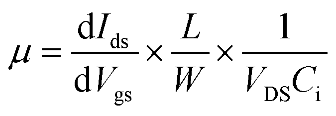 .
.
 | ||
| Scheme 1 Schematic diagram of the fabrication process of R2R gravure printed (a) top-gated and (b) bottom-gated SWCNT TFTs and CMOS inverters on flexible substrates including PET, Al, and paper. | ||
3. Results and discussion
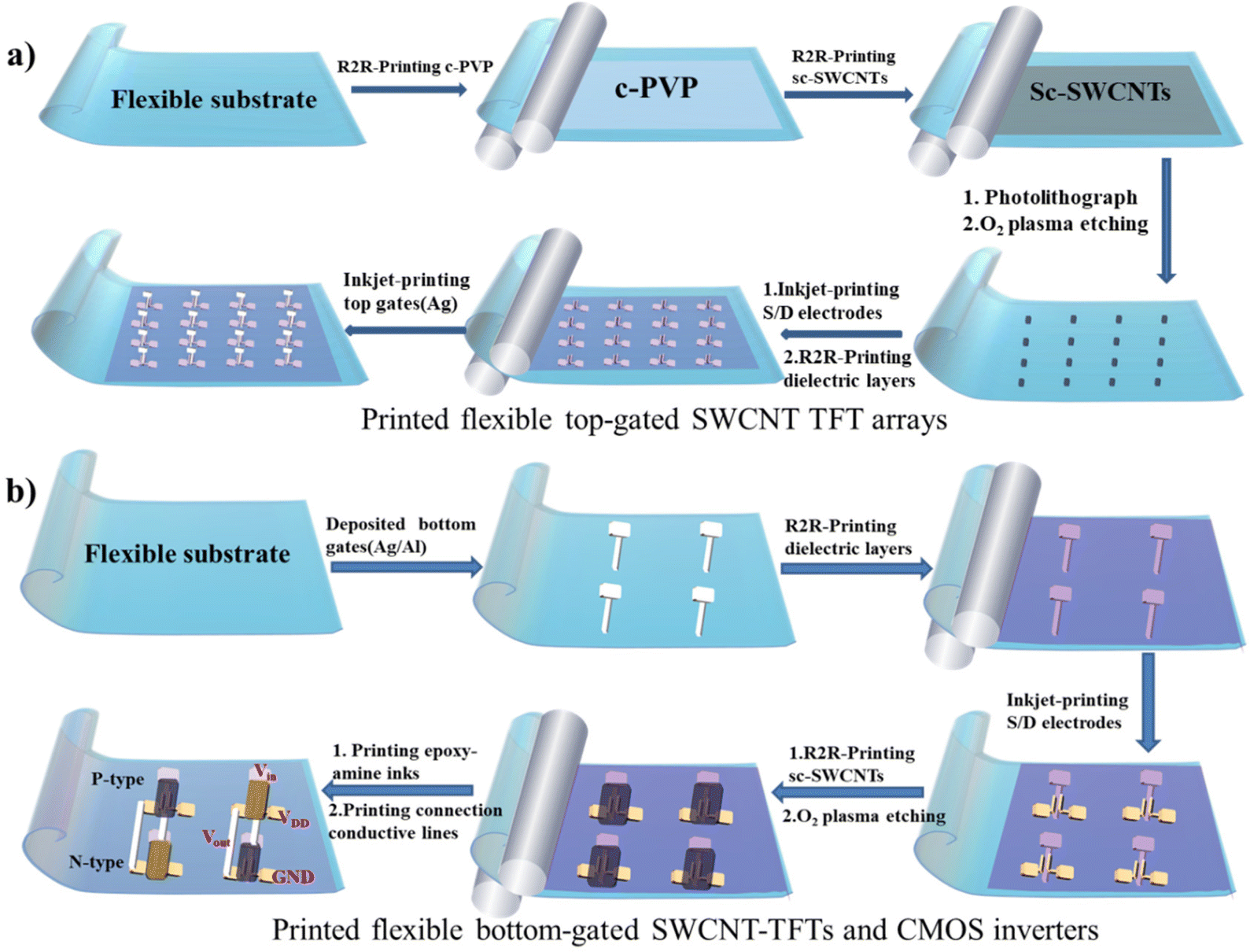
Generally, the as-prepared polymer-sorted sc-SWCNT inks are unsuitable for R2R gravure printing due to low-concentration sc-SWCNTs and high-concentration polymers in inks. To meet the requirements of R2R gravure printing, PCz-sorted sc-SWCNT inks (the sc-SWCNT absorbance peak height of ∼0.3) were filtered using a 0.2 µm filter, and the filtered sc-SWCNT thin films were cleaned with toluene and then redispersed in toluene to obtain highly concentrated sc-SWCNT inks (the sc-SWCNT absorbance peak height of 1.8 and 4.5 for ink 2 and 3 is shown in Fig. 1). It can be seen from Fig. 1b that the S22 peaks (1000–1200 nm) of the sc-SWCNTs have a sharp peak, and no metal peaks (600–800 nm) are observed. Notably, the peak heights of PCz polymers in sc-SWCNT ink 2 with an sc-SWCNT absorbance peak height of 1.8 are lower than those in the as-sorted sc-SWCNTs with an sc-SWCNT absorbance peak height of 0.3 after filtering, indicating that filtering could effectively remove free PCz polymers in sc-SWCNT inks. The excess polymers in TFT channels could severely hinder the carrier transport in the sc-SWCNT network and reduce the Ion/Ioff ratios of SWCNT TFTs. Later experiments show that the sc-SWCNT inks prepared by this method greatly simplify the fabrication process of TFTs, and excellent electrical properties are obtained without solvent cleaning.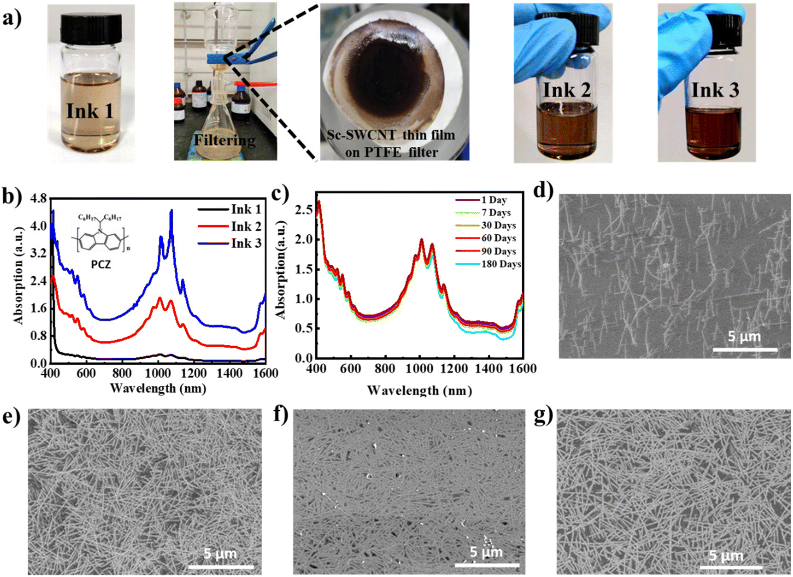 | ||
| Fig. 1 (a) Optical images of sorted and concentrated sc-SWCNT inks and sc-SWCNT thin film on the PTFE substrate, (b) UV-vis-NIR adsorption spectra of sorted and concentrated sc-SWCNT inks, (c) UV-vis-NIR adsorption spectra of ink 2 with the adsorption peak height of 1.8 after storage for 100 days. SEM images of R2R gravure printed SWCNT thin films on PVP-modified PET substrates (the printing speed of 8 m min−1, the printing pressure of 73%, and printing 10 times) using sc-SWCNT inks with the adsorption peak heights of (d) 0.3, (e) 1.8, (f) 3.8, and (g) 1.8 after storage for 30 days. | ||
The stability of the concentrated inks is also investigated. It can be seen from Fig. 1c that the highly concentrated sc-SWCNT ink 2 still has excellent dispersion after storage in air for 180 days. The inks 1–3 with a surface tension of 30–35 mN m−1 and a viscosity of 27–30 Cp could provide rheology and adequate ink transferring at a processing speed of 8–12 m min−1 during R2R gravure printing without the addition of binders or surfactants, which can adversely affect the electrical properties of SWCNT TFTs. To evaluate the quality of printing sc-SWCNT thin films, inks 1–3 were R2R gravure printed on c-PVP-modified PET substrates 10 times and the morphologies of sc-SWCNT thin films were characterized by SEM as shown in Fig. 1d–g. It was obvious that high-density sc-SWCNT thin films were observed using the highly concentrated sc-SWCNT inks 2 and 3 after R2R gravure printing 10 times. However, inks with higher concentrations have more sc-SWCNT bundles and polymer residues (Fig. 1b and f), which seriously degrade the electrical properties of sc-SWCNT TFTs. Fig. 1g shows that R2R gravure printed sc-SWCNT thin films are still dense and homogeneous when using ink 2 stored in air for 30 days, demonstrating good long-term stability of the enriched sc-SWCNT ink 2.
To investigate the generalizability of R2R printing of large-area sc-SWCNT thin films on different substrates, we also chose paper substrates and Al foils. It is noteworthy that we attempted to deposit sc-SWCNTs on commercial Al foil (fabricated by R2R techniques) with the aim of simplifying the fabrication process by using the Al foil directly as the low work function gate electrode for the fabrication of enhancement-mode P-type SWCNT TFTs. Fig. 2 demonstrates the typical SEM images of sc-SWCNT networks on PET, paper, and Al substrates before and after the modification of the c-PVP adhesion layer. It can be seen that few sc-SWCNTs could be observed on substrates without the c-PVP adhesion layer, due to the weak bonding force between sc-SWCNTs and substrates (Fig. 2a–c). On the other hand, high-density and uniform sc-SWCNT thin films were achieved on c-PVP-modified substrates (Fig. 2d–f). The density of sc-SWCNTs could reach ∼60 tubes μm−1 on the c-PVP-modified Al and PET substrates, while the density reduced to ∼30 tubes μm−1 on the c-PVP-modified paper substrates due to the uneven and porous surface. The insets of Fig. 2 show the water contact angles on the corresponding substrates. The water contact angles on PET, Al, and paper substrates without the c-PVP adhesion layer were 64.9°, 53.5°, and 81.4°, respectively (inset of Fig. 2a–c). After being modified with c-PVP thin films, the water contact angles on these substrates decreased to 11.6°, 6.8°, and 20.1°, respectively (inset of Fig. 2d–f). It was attributed to hydroxyl groups on the c-PVP-modified substrates. The SEM and water contact angle results reveal that the c-PVP thin films can act as the adhesion layer to immobilize sc-SWCNTs efficiently, and high-density sc-SWCNT networks were achieved after the modification of the c-PVP adhesion layer. It is noteworthy that some functional groups such as –OH, C–O, –COO– and C![[double bond, length as m-dash]](https://www.rsc.org/images/entities/char_e001.gif) O would be formed on PVP substrates after treatment with oxygen plasma and are helpful for immobilizing sorted sc-SWCNTs on the c-PVP surfaces of different substrates, probably via strong intermolecular forces (hydrogen bonding/van der Waals/electrostatic force). Therefore, ink 2 and c-PVP thin films are chosen as the R2R printing semiconducting ink and the adhesion layers to immobilize sc-SWCNTs in the following experiments.
O would be formed on PVP substrates after treatment with oxygen plasma and are helpful for immobilizing sorted sc-SWCNTs on the c-PVP surfaces of different substrates, probably via strong intermolecular forces (hydrogen bonding/van der Waals/electrostatic force). Therefore, ink 2 and c-PVP thin films are chosen as the R2R printing semiconducting ink and the adhesion layers to immobilize sc-SWCNTs in the following experiments.
 | ||
| Fig. 2 SEM images of sc-SWCNT films on (a) Al, (b) PET, and (c) paper substrates without the c-PVP modification layer, and (d) Al, (e) PET and (f) paper substrates with c-PVP modification after R2R printing 10 times. The insets are water contact angles of Al, PET, and paper substrates before and after the modification of c-PVP thin films by R2R gravure printing. | ||
To investigate the feasibility of R2R gravure printing in fabricating large-area devices, sc-SWCNT thin film deposition on an 8 cm × 14 cm PET substrate was explored. Firstly, the c-PVP adhesion layer was deposited on flexible substrates by R2R gravure printing at a speed of 11 m min−1, and then ink 2 was R2R gravure printed on c-PVP-modified flexible substrates 10 times at a printing speed of 8 m min−1. As shown in Fig. 3, dense and uniform sc-SWCNT networks could be obtained in different areas of 8 cm × 14 cm on the PET substrate after R2R gravure printing sc-SWCNT inks 10 times with a single printing time of 0.1 ms. The results indicated that R2R gravure printing high-purity sc-SWCNTs on flexible substrates is scalable and has the potential for future applications in large-area flexible electronic devices.
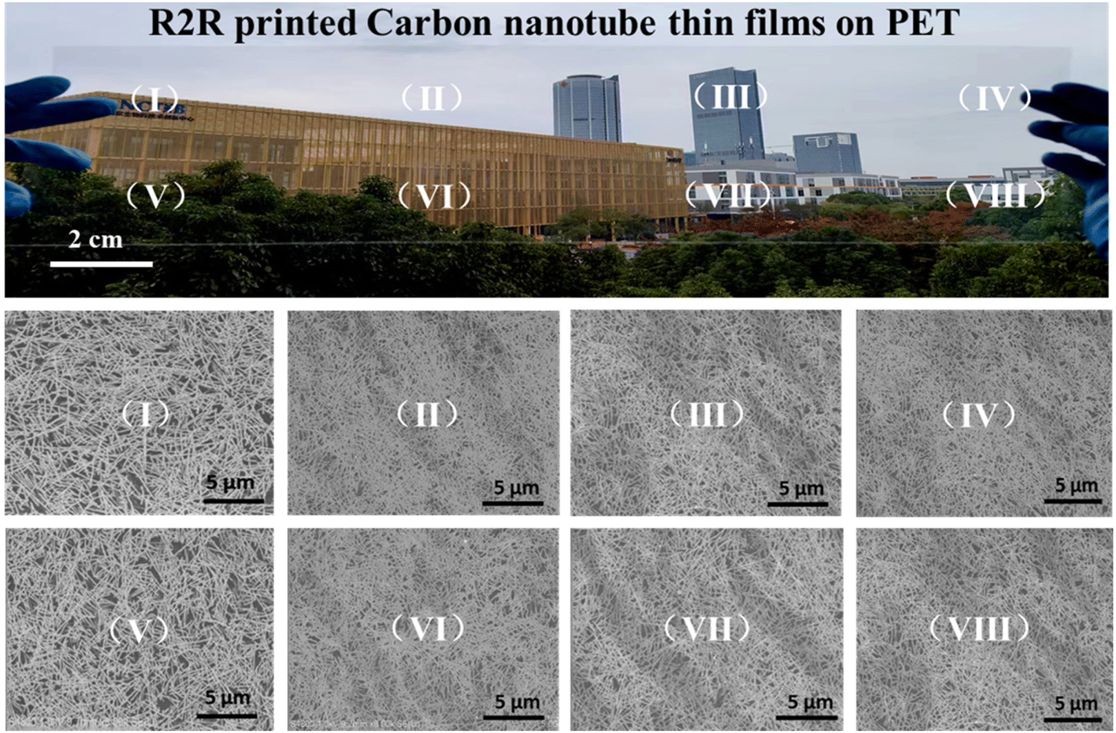 | ||
| Fig. 3 SEM images of sc-SWCNT networks in different areas of 8 cm × 14 cm sc-SWCNT thin films on a PET substrate. | ||
To obtain high-quality R2R printed sc-SWCNT thin films for high-performance TFT devices, 5, 10, 12, and 15 active layers on c-PVP-modified PET substrates were R2R printed with ink 2, and the top-gated printed SWCNT TFTs were then constructed, and electrical properties were evaluated. Fig. 4a–c and 3 display the sparse carbon nanotube networks for printing 5, 10, 12, and 15 times. Obviously, the density of sc-SWCNT thin films increases with increasing printing times. At the same time, more carbon nanotube bundles and polymers in sc-SWCNT thin films were observed as shown in Fig. 4b and c, which can block carrier transports in carbon nanotube networks. The corresponding electrical characteristics of sc-SWCNT TFTs are displayed in Fig. 4d–f. It can be seen from Fig. 4d that the on-currents of printed SWCNT TFTs increased with increasing sc-SWCNT printing times due to the increasing sc-SWCNT density in the TFT channels, and the Ion/Ioff ratios, μFE, hysteresis, and SS decrease when the printing times are more than 10 times. As shown in Fig. 4d–f, the optimum Ion/Ioff ratio (106), μFE (11.9 cm2 V−1 s−1), hysteresis (ΔVHYST ∼ 30 mV) and SS (70 mV dec−1) of the printed SWCNT TFTs were obtained when R2R printing 10 times. However, further increasing printing sc-SWCNT ink times could decrease the electrical properties of the printed SWCNT TFTs, which is ascribed to the carrier transport being affected by the formation of sc-SWCNT bundles and the increased polymers in SWCNT thin films.
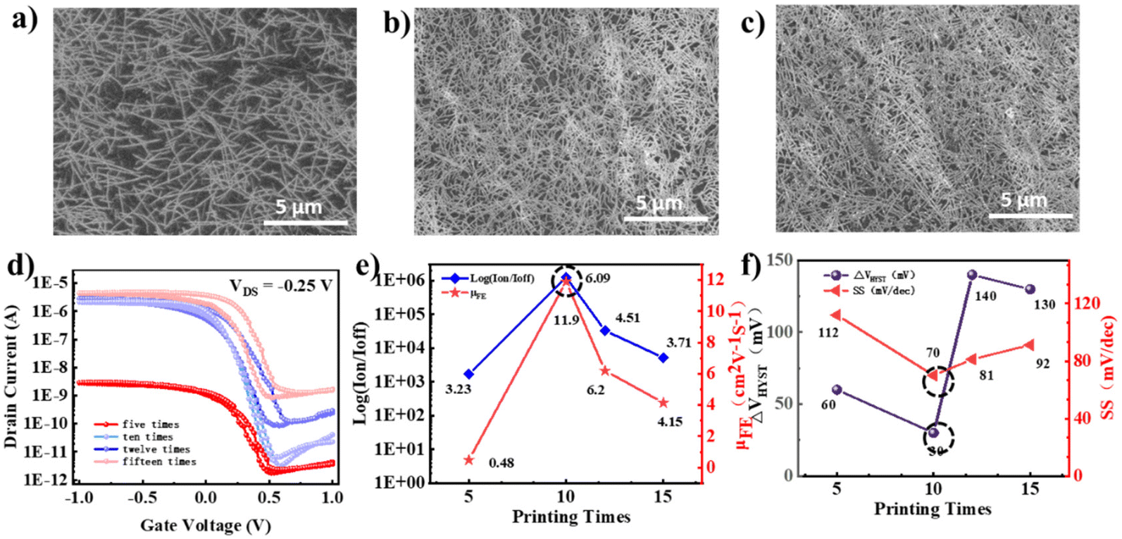 | ||
| Fig. 4 SEM images of R2R gravure printed SWCNT thin films with different printing times using sc-SWCNT inks with the adsorption peak height of 1.8. (a) 5 times, (b) 12 times, and (c) 15 times, (d) the corresponding transfer curves, (e) calculated Ion/Ioff and µFE, and (f) SS and ΔVHYST of fully printed SWCNT-TFTs. | ||
Fig. 5a and b illustrate the fully printed top-gated SWCNT TFT arrays and the SEM images of sc-SWCNT channels on PET and paper substrates, respectively. The transfer characteristics of the as-prepared SWCNT-TFTs on PET and paper substrates are shown in Fig. 5c–h. All devices exhibited typical p-type behavior due to the adsorption of oxygen and moisture from the ambient environment at the channel area and excellent mechanical flexibility after bending 10000 or 5000 times with a curvature radius of 5 mm. It is noteworthy that the printed SWCNT TFTs on PET substrates show more excellent electrical properties (higher Ion/Ioff ratios, mobility, and smaller SS) than those on paper substrates. It can be observed from the optical image in Fig. 5b that the surface of the paper substrate is very rough and porous, resulting in unclean etching during the patterning of sc-SWCNT thin films by oxygen plasma and higher off currents than those on other substrates. Table 1 summarizes the electrical parameters extracted from the transfer curves of the fully printed SWCNT TFTs on the PET and paper substrates (12 devices), exhibiting satisfactory electrical properties. The printed SWCNT TFTs on PET substrates had a low threshold voltage, a high Ion/Ioff ratio (≥106), a small SS (70–80 mV dec−1), and small hysteresis (ΔVHYST = 40 ± 5 mV), as well as a high carrier mobility (μFE = 9.79 ± 0.5 cm2 V−1 s−1) at low gate voltages (±1 V). Although the rough and porous structure of paper substrates led to decreased Ion/Ioff ratios of TFTs, SWCNT TFTs on paper substrates still have a small SS (∼78 mV dec−1) and a high μFE (∼4.53 cm2 V−1 s−1).
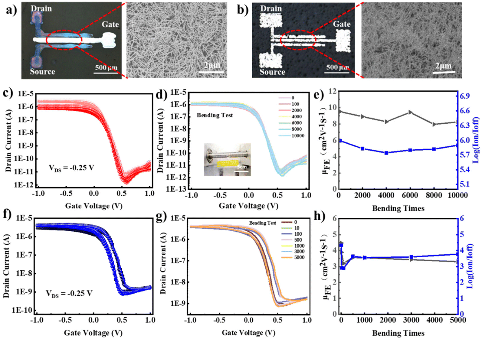 | ||
| Fig. 5 Optical images of fully printed SWCNT TFTs and the SEM images of sc-SWCNT thin films in device channels on (a) PET and (b) paper substrates. (c) Transfer curves of fully printed SWCNT TFTs on the PET substrate, and (d) and (e) mechanical flexibility properties after bending 10000 times with a curvature radius of 5 mm (VDS = −0.25 V). (f) Transfer curves of fully printed SWCNT TFTs on paper substrates, and (g) and (h) mechanical flexibility properties after bending 5000 times with a curvature radius of 5 mm (VDS = −0.25 V). The inset in (d) is the photograph of the flexible devices wrapped on a cylinder with a curvature radius of 5 mm. | ||
| Substrate | SS (mV dec−1) | ΔVHYST (mV) | I on/Ioff | μ FE (cm2 V−1 s−1) |
|---|---|---|---|---|
| PET | 72 ± 5 | 40 ± 5 | ∼106 | 9.79 ± 0.5 |
| Paper | 78 ± 6 | 140 ± 10 | 10 3 –10 4 | 4.53 ± 0.8 |
The mechanical bending tests were performed to evaluate the mechanical stability of the fully printed top-gated SWCNT TFTs on PET and paper substrates. Fig. 5d shows the measured transfer curves of the fully printed SWCNT TFTs on the PET substrate after 10000 bending cycles. No significant electrical property (µFE and Ion/Ioff) degradation was observed after 10000 bending cycles. Fig. 5e displays the bending time as a function of extracted µFE and Ion/Ioff ratios; no significant electrical property degradation was observed after 10000 bending cycles. The outstanding mechanical flexibility and reliability of the fully printed SWCNT TFTs on PET substrates can be attributed to the mechanical compatibility of IL-c-PVP solid-state electrolytes and the mechanical flexibility of sc-SWCNTs, as well as the excellent bending resistance of the PET substrate. Fig. 5f–h show the measured transfer curves of the fully printed SWCNT TFTs on the paper substrate after 5000 bending cycles. No significant changes were observed after bending 5000 cycles. However, the Ion decreased, and the transfer curves became unsmooth when further increasing the number of bending cycles.
To facilitate the development of CMOS circuits, we developed R2R bottom-gated SWCNT TFTs with a similar manufacturing process (Scheme 1b). It is known that enhancement-mode TFTs can be obtained by reducing the work function of the gate electrodes.38 The enhancement-mode and depletion-mode bottom-gate/top contact TFTs were obtained when using the Al gate electrodes with low work function native aluminum oxide (as a result, the holes in the TFT channel were depleted, and a negative threshold voltage shift was observed) and the silver gate electrodes are shown in Fig. 6a–c. It can be seen from Fig. 5c and 6c that both the Ion/Ioff ratios and mobility of bottom-gated SWCNT TFTs are similar to those of top-gated SWCNT TFTs. N-type SWCNT TFTs were achieved by covering the epoxy-amine inks on the channel of p-type TFTs (Fig. 6d). The prepared p-type and n-type SWCNT TFTs exhibited almost symmetric electrical properties in the ambient environment (Fig. 6e). It is worth noting that the Ion of the SWCNT-TFTs during the polarity transition remained unchanged. This is due to the solidified state of the polarization transfer solution and low air and water oxygen density in the environment.
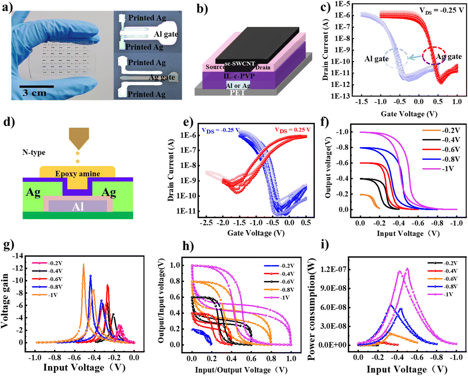 | ||
| Fig. 6 (a) Optical and magnified optical images of printed SWCNT TFTs, (b) the structure of a printed bottom-gated printed SWCNT TFT, (c) typical transfer characteristics of fully printed Ag-gate SWCNT TFTs and Al-gate SWCNT TFTs on PET substrates. (d) The structure of a printed n-type bottom-gated printed SWCNT TFT, (e) transfer characteristics of p-type and n-type SWCNT TFTs with VDS = −0.25 V and 0.25 V, respectively. (f) Input/output voltage curves, (g) voltage gains, (h) noise tolerance, and (i) power consumption of the printed CMOS inverter with input voltages from −0.2 V to −1 V. | ||
To demonstrate the potential of R2R gravure printed high-speed, large-area, low-cost SWCNT TFTs for the realization of ultra-low voltage CMOS circuits in the fields of electronic skin, flexible neuromorphic devices, and intelligent wearable devices and systems, printed SWCNT CMOS inverters were constructed by connecting two unipolar n-type and p-type TFTs, as shown in Fig. 6e. The performance of p-type and n-type SWCNT TFTs used in the CMOS inverter is shown in Scheme 1b. The voltage gain, power dissipation, and noise margins were extracted from the static inverter characteristics to evaluate whether the printed CMOS inverters are suitable for integrating complicated and high-performance logic circuits with low power consumption. Fig. 6f indicates that the printed CMOS inverters exhibited full rail-to-rail voltage operation with VDD down to −0.2 V. As shown in Fig. 6g, the voltage gains (dVout/dVin) of the printed CMOS inverters were 10.8 and 12.8 at VDD = −0.8 V and VDD = −1 V, respectively. The noise margins of the printed CMOS inverter with input voltages from −0.4 V to −1 V are 38%, 50%, 56%, 60% of 1/2 VDD (Fig. 6h). Another important feature of the portable devices is the power dissipation (PW = IDD × VDD), as demonstrated in Fig. 6i. The power dissipation of the printed CMOS inverters was 0.51 nW at VDD = −0.4 V, and the lowest power consumption 0.056 nW was achieved at VDD = −0.2 V. It is noteworthy that the as-prepared enhancement-mode p-type and n-type SWCNT TFTs exhibited almost symmetric electrical properties with low off-currents and low leakage currents and the printed CMOS inverters exhibited full rail-to-rail voltage operation. Such a low power consumption could be attributed to the well-matched CMOS TFTs with relatively low off-currents and low leakage currents (∼10−10 A).
4. Conclusion
In summary, we developed a universal approach for constructing large area and high-quality sc-SWCNT thin films on flexible substrates (PET, paper, and Al substrates) by R2R gravure printing using highly concentrated sc-SWCNT inks and c-PVP films as the adhesion layer. The fully printed flexible SWCNT TFTs based on R2R gravure printed sc-SWCNT thin films exhibited excellent mechanical flexibility and good electrical properties with a high Ion/Ioff ratio (∼106), a small SS (∼70 mV dec−1), small hysteresis, and a high carrier mobility (∼11.9 cm2 V−1 s−1) at a gate voltage between −1 V and 1 V. Moreover, the fully printed inverters exhibited rail-to-rail output swings with a voltage gain of up to 12.8 at VDD = −1 V and the power consumption down to 0.056 nW at VDD = −0.2 V. Overall, this work overcame the performance, cost, size, and efficiency limitations of conventional materials and printing methods, which could promote the development of fully printed low-cost, large-area, high-output, and flexible carbon-based electronics. To meet the demands of R2R gravure printing, we will focus on developing directly patternable sc-SWCNT inks using high viscosity, highly polar and low toxicity solvents and optimizing the R2R gravure printing process.Conflicts of interest
The authors declare no competing financial interest.Acknowledgements
This work was supported by the National Natural Science Foundation of China (62274174) and the National Key Research and Development Program of China (2020YFA0714700). The authors are grateful for the technical support for Nano-X from Suzhou Institute of Nano-Tech and Nano-Bionics, Chinese Academy of Sciences (SINANO) (F2208).References
- M. Saadi, A. Maguire, N. T. Pottackal, M. S. H. Thakur, M. M. Ikram, A. J. Hart, P. M. Ajayan and M. M. Rahman, Adv. Mater., 2022, 34, 2108855 CrossRef CAS.
- F. Liao, J. Deng, X. Chen, Y. Wang, X. Zhang, J. Liu, H. Zhu, L. Chen, Q. Sun, W. Hu, J. Wang, J. Zhou, P. Zhou, D. W. Zhang, J. Wan and W. Bao, Small, 2020, 16, 1904369 CrossRef CAS.
- A. Liu, H. Zhu, S. Bai, Y. Reo, T. Zou, M.-G. Kim and Y.-Y. Noh, Nat. Electron., 2022, 5, 78–83 CrossRef CAS.
- J.-L. Meng, T.-Y. Wang, L. Chen, Q.-Q. Sun, H. Zhu, L. Ji, S.-J. Ding, W.-Z. Bao, P. Zhou and D. W. Zhang, Nano Energy, 2021, 83, 105815 CrossRef CAS.
- A. Corletto and J. G. Shapter, ACS Appl. Nano Mater., 2020, 3, 8148–8160 CrossRef CAS.
- W. Gao, S. Emaminejad, H. Y. Y. Nyein, S. Challa, K. Chen, A. Peck, H. M. Fahad, H. Ota, H. Shiraki, D. Kiriya, D. H. Lien, G. A. Brooks, R. W. Davis and A. Javey, Nature, 2016, 529, 509–514 CrossRef CAS.
- A. A. Marunchenko, M. A. Baranov, E. V. Ushakova, D. R. Ryabov, A. P. Pushkarev, D. S. Gets, A. G. Nasibulin and S. V. Makarov, Adv. Funct. Mater., 2021, 32, 2109834 CrossRef.
- K. Schnittker, M. Tursunniyaz and J. B. Andrews, J. Inf. Disp., 2021, 22, 193–209 CrossRef.
- H. Y. Y. Nyein, M. Bariya, B. Tran, C. H. Ahn, B. J. Brown, W. Ji, N. Davis and A. Javey, Nat. Commun., 2021, 12, 1823 CrossRef CAS.
- J. Pang, A. Bachmatiuk, F. Yang, H. Liu, W. Zhou, M. H. Rummeli and G. Cuniberti, Nano-Micro Lett., 2021, 13, 191 CrossRef CAS.
- Y. Tchoe, J. Lee, R. Liu, A. M. Bourhis, R. Vatsyayan, K. J. Tonsfeldt and S. A. Dayeh, Appl. Phys. Rev., 2021, 8, 041317 CAS.
- S. Qiu, K. Wu, B. Gao, L. Li, H. Jin and Q. Li, Adv. Mater., 2019, 31, 1800750 CrossRef.
- T. Gao, J. Deng, X. Li, Y. Ren, W. Gu, M. Robin and J. Zhao, J. Mater. Chem. C, 2021, 9, 6852–6862 RSC.
- E. Li, C. Gao, R. Yu, X. Wang, L. He, Y. Hu, H. Chen, H. Chen and T. Guo, Nat. Commun., 2022, 13, 2898 CrossRef CAS PubMed.
- P. Schulz, A. M. Dowgiallo, M. Yang, K. Zhu, J. L. Blackburn and J. J. Berry, J. Phys. Chem. Lett., 2016, 7, 418–425 CrossRef CAS.
- R. Shiwaku, H. Matsui, K. Hayasaka, Y. Takeda, T. Fukuda, D. Kumaki and S. Tokito, Adv. Electron. Mater., 2017, 3, 1600557 CrossRef.
- C. Du, Y. Ren, Z. Qu, L. Gao, Y. Zhai, S. T. Han and Y. Zhou, Nanoscale, 2021, 13, 7498–7522 RSC.
- D. Fong, W. J. Bodnaryk, N. A. Rice, S. Saem, J. M. Moran-Mirabal and A. Adronov, Chem. – Eur. J., 2016, 22, 14560–14566 CrossRef CAS.
- D. Heimfarth, M. B. Leinen, P. Klein, S. Allard, U. Scherf and J. Zaumseil, ACS Appl. Mater. Interfaces, 2022, 14, 8209–8217 CrossRef CAS.
- D. Kiriya, K. Chen, H. Ota, Y. Lin, P. Zhao, Z. Yu, T. J. Ha and A. Javey, Am. Chem. Soc., 2014, 136, 11188–11194 CrossRef CAS.
- J. Lefebvre, J. Ding, Z. Li, P. Finnie, G. Lopinski and P. R. L. Malenfant, Acc. Chem. Res., 2017, 50, 2479–2486 CrossRef CAS.
- F. Li, H. Wang, D. Kufer, L. Liang, W. Yu, E. Alarousu, C. Ma, Y. Li, Z. Liu, C. Liu, N. Wei, F. Wang, L. Chen, O. F. Mohammed, A. Fratalocchi, X. Liu, G. Konstantatos and T. Wu, Adv. Mater., 2017, 29, 1602432 CrossRef.
- M. Si, Z. Lin, Z. Chen, X. Sun, H. Wang and P. D. Ye, Nat. Electron., 2022, 5, 164–170 CrossRef CAS.
- X. Wang, M. Zhu, X. Li, Z. Qin, G. Lu, J. Zhao and Z. Zhang, Adv. Mater., 2022, 34, 2204066 CrossRef CAS.
- M. Li, Z. Xiong, S. Shao, L. Shao, S.-T. Han, H. Wang and J. Zhao, Carbon, 2021, 176, 592–601 CrossRef CAS.
- X. Li, Y. Ren, X. Wang, S. Shao, H. Li, L. Wu, X. Liu and J. Zhao, Adv. Electron. Mater., 2021, 7, 2001025 CrossRef CAS.
- X. Li, X. Wang, J. Deng, M. Li, S. Shao and J. Zhao, Carbon, 2022, 191, 267–276 CrossRef CAS.
- Z. Li, J. Ding, F. Lapointe and P. R. L. Malenfant, J. Mater. Sci.: Mater. Electron., 2021, 32, 23923–23934 CrossRef CAS.
- Y. Ren, M. Li, X. Li, Y. Geng, X. Wang and J. Zhao, J. Mater. Chem. C, 2021, 9, 2133–2144 RSC.
- M. Song, Y. Sun, Z. Liu, B. Wei, H. Wang, J. Yuan, Y. Chen, X. Yang and D. Xie, Carbon, 2021, 184, 295–302 CrossRef CAS.
- W. Xu, M. Li, M. Tange, L. Li, J. Hou, J. Ye, L. Wei, Y. Chen and J. Zhao, Nano Res., 2022, 15, 5517–5526 CrossRef CAS.
- J. Deng, X. Li, M. Li, X. Wang, S. Shao, J. Li, Y. Fang and J. Zhao, Nanoscale, 2022, 14, 4679–4689 RSC.
- J. K. Han, J. Oh, G. J. Yun, D. Yoo, M. S. Kim, J. M. Yu, S. Y. Choi and Y. K. Choi, Sci. Adv., 2021, 7, 8836 CrossRef.
- S. Schneider, J. M. Gotthardt, L. Steuer, S. Leingang, H.-J. Himmel and J. Zaumseil, J. Mater. Chem. C, 2021, 9, 7485–7493 RSC.
- J. A. Cardenas, J. B. Andrews, S. G. Noyce and A. D. Franklin, Nano Futures, 2020, 4, 012001 CrossRef CAS.
- Y. Geng, Y. Ren, X. Wang, J. Li, L. Portilla, Y. Fang and J. Zhao, Sens. Actuators, B, 2022, 360, 131633 CrossRef CAS.
- T. Pandhi, A. Chandnani, H. Subbaraman and D. Estrada, Sensors, 2020, 20, 5642 CrossRef CAS.
- X. Wang, M. Wei, X. Li, S. Shao, Y. Ren, W. Xu, M. Li, W. Liu, X. Liu and J. Zhao, ACS Appl. Mater. Interfaces, 2020, 12, 51797–51807 CrossRef CAS.
- M. Ben Basat and N. Lachman, Nanomaterials, 2021, 11, 2618 CrossRef CAS PubMed.
- F. Cao and L. Li, Adv. Funct. Mater., 2020, 31, 2008275 CrossRef.
- S. Lu and A. D. Franklin, Nanoscale, 2020, 12, 23371–23390 RSC.
- L. Wu, Y. Yu and J. Zhi, RSC Adv., 2015, 5, 10159–10164 RSC.
- Y. Y. Kim, T. Y. Yang, R. Suhonen, A. Kemppainen, K. Hwang, N. J. Jeon and J. Seo, Nat. Commun., 2020, 11, 5146 CrossRef CAS.
- J. Sun, H. Park, Y. Jung, G. Rajbhandari, B. B. Maskey, A. Sapkota, Y. Azuma, Y. Majima and G. Cho, ACS Omega, 2017, 2, 5766–5774 CrossRef CAS.
- A. M. Tiara, H. Moon, G. Cho and J. Lee, Jpn. J. Appl. Phys., 2022, 61, SE0802 CrossRef.
- Q. Cao, Nano Res., 2021, 14, 3051–3069 CrossRef CAS.
- M. Choi, B. Jang, W. Lee, S. Lee, T. W. Kim, H.-J. Lee, J.-H. Kim and J.-H. Ahn, Adv. Funct. Mater., 2017, 27, 1606005 CrossRef.
- J. Noh, K. Jung, J. Kim, S. Kim, S. Cho and G. Cho, IEEE Electron Device Lett., 2012, 33, 1574–1576 CAS.
- Y. Jung, J. Park, J. Sun, H. Park, S. Parajuli, S. Shrestha, K. Shrestha, Y. Majima and G. Cho, Adv. Mater. Technol., 2021, 7, 2101243 CrossRef.
- W. Lee, H. Koo, J. Sun, J. Noh, K. S. Kwon, C. Yeom, Y. Choi, K. Chen, A. Javey and G. Cho, Sci. Rep., 2015, 5, 17707 CrossRef CAS.
- J. Sun, A. Sapkota, H. Park, P. Wesley, Y. Jung, B. B. Maskey, Y. Kim, Y. Majima, J. Ding, J. Ouyang, C. Guo, J. Lefebvre, Z. Li, P. R. L. Malenfant, A. Javey and G. Cho, Adv. Electron. Mater., 2020, 6, 1901431 CrossRef CAS.
- Z. Zhang, B. Wang, J. Qiu and S. Wang, Manuf. Lett., 2019, 21, 28–34 CrossRef.
- C. M. Homenick, R. James, G. P. Lopinski, J. Dunford, J. Sun, H. Park, Y. Jung, G. Cho and P. R. L. Malenfant, ACS Appl. Mater. Interfaces, 2016, 8, 27900–27910 CrossRef CAS.
- Q. Zhang, Y. Ren, Z. Wang, X. Chen, L. Portilla, L. Sun, D. Zhang and J. Zhao, Flexible Printed Electron., 2022, 7, 015007 CrossRef.
- J. Sun, K. Shrestha, H. Park, P. Yadav, S. Parajuli, S. Lee, S. Shrestha, G. R. Koirala, Y. Kim, K. A. Marotrao, B. B. Maskey, O. C. Olaoluwa, J. Park, H. Jang, N. Lim, Y. Jung and G. Cho, Adv. Mater. Technol., 2019, 5, 1900935 CrossRef.
- H. Koo, W. Lee, Y. Choi, J. Sun, J. Bak, J. Noh, V. Subramanian, Y. Azuma, Y. Majima and G. Cho, Sci. Rep., 2015, 5, 14459 CrossRef CAS.
- J. Noh, J. Minhun, J. Kyunghwan, L. Gwangyong, K. Joonseok, L. Soyeon, K. Daae, C. Youngchul, K. Yoonjin, V. Subramanian and C. Gyoujin, IEEE Electron Device Lett., 2011, 32, 638–640 CAS.
Footnote |
| † Electronic supplementary information (ESI) available. See DOI: https://doi.org/10.1039/d2nr07209b |
| This journal is © The Royal Society of Chemistry 2023 |