
Room-temperature spin-valve devices based on Fe3GaTe2/MoS2/Fe3GaTe2 2D van der Waals heterojunctions†
Wen
Jin
ab,
Gaojie
Zhang
ab,
Hao
Wu
abcd,
Li
Yang
ab,
Wenfeng
Zhang
 abc and
Haixin
Chang
*abcd
abc and
Haixin
Chang
*abcd
aCenter for Joining and Electronic Packaging, State Key Laboratory of Material Processing and Die & Mold Technology, School of Materials Science and Engineering, Huazhong University of Science and Technology, Wuhan 430074, China. E-mail: hxchang@hust.edu.cn
bShenzhen R&D Center of Huazhong University of Science and Technology (HUST), Shenzhen 518000, China
cInstitute for Quantum Science and Engineering, Huazhong University of Science and Technology, Wuhan 430074, China
dWuhan National High Magnetic Field Center, Huazhong University of Science and Technology, Wuhan 430074, China
First published on 6th February 2023
Abstract
The spin-valve effect has been the focus of spintronics over the last decades due to its potential for application in many spintronic devices. Two-dimensional (2D) van der Waals (vdW) materials are highly efficient to build spin-valve heterojunctions. However, the Curie temperatures (TC) of the vdW ferromagnetic (FM) 2D crystals are mostly below room temperature (∼30–220 K). It is very challenging to develop room-temperature, FM 2D crystal-based spin-valve devices. Here, we report room-temperature, FM 2D-crystal-based all-2D vdW Fe3GaTe2/MoS2/Fe3GaTe2 spin-valve devices. The magnetoresistance (MR) of the device was up to 15.89% at 2.3 K and 11.97% at 10 K, which are 4–30 times the MR of the spin valves of Fe3GeTe2/MoS2/Fe3GeTe2 and conventional NiFe/MoS2/NiFe. The typical spin valve effect showed strong dependence on the MoS2 spacer thickness in the vdW heterojunction. Importantly, the spin valve effect (0.31%) robustly existed even at 300 K with low working currents down to 10 nA (0.13 A cm−2). This work provides a general vdW platform to develop room-temperature, 2D FM-crystal-based 2D spin-valve devices.
1. Introduction
The spin-valve effect has been the focus of spintronics over the last decades due to its application in magnetoresistance sensors,1–3 magnetic random-access memory4,5 and read heads for high-density magnetic recording.6,7 Typically, spin-valve devices consist of two ferromagnetic (FM) electrodes separated by a nonmagnetic spacer layer. Traditional ferromagnets, such as Fe,8 NiFe,9 Co10 or CoFeB,11 have been extensively investigated as FM electrodes in spin-valve devices. To obtain a well-defined interface regardless of lattice mismatch, two-dimensional (2D) van der Waals (vdW) materials are considered highly suitable to build spin-valve heterojunctions due to their perfectly flat surface without any dangling bonds.12–17Over the past few years, 2D vdW materials have been theoretically and experimentally demonstrated as non-magnetic spacer layers based on the tunneling or spin-valve effect because they yield large tunneling magnetoresistance (TMR) or magnetoresistance (MR). Different types of spacer layers contribute to different physical mechanisms in the devices. In BN-based spin-valve devices, high TMR was obtained when BN served as a tunneling barrier.18 In Fe3GeTe2/graphite/Fe3GeTe2 heterostructures, an antisymmetric three-state MR effect was observed, revealing spin-momentum locking caused by the SOC-induced Rashba-split 2D electron gas at the Fe3GeTe2/graphite interface.19 Moreover, transition-metal dichalcogenide (TMDC) semiconductors are another kind of promising candidates for non-magnetic spacer layers due to their fascinating physical properties.20,21 Under the influence of different thicknesses or defects, the TMDC semiconductors play two different roles in the spin-valve heterojunctions as the conducting or tunneling layer. For example, the spacers in NiFe/MoS2/NiFe,22 NiFe/WSe2/NiFe23 and Fe3GeTe2/MoS2/Fe3GeTe224 act as conducting layers, while in the Fe3GeTe2/WSe2/Fe3GeTe225 heterojunction, WSe2 acts as the tunneling layer. Despite these TMDC semiconductors, including MoS2, as the spacer layers have been reported, room-temperature all-2D vdW MoS2-based spin valves are still rare, making it critical to realize room-temperature FM in 2D vdW materials for the practical application of 2D spin-valve devices in spintronics.
Theoretically, long-range ferromagnetism hardly exists in 2D materials because of thermal fluctuations,26 which, meanwhile, can be stabilized by the excitation gap induced by magnetic anisotropy.27 To date, progress has been made in the research of intrinsic 2D FM crystals, such as CrI3,28 Cr2Ge2Te627 and Fe3GeTe2,29 but the Curie temperatures (TC) of these FM 2D crystals are mostly below the room temperature (∼30–220 K), which can hinder their practical room-temperature application in next-generation spin-valve spintronic devices. Recently, the emergence of Fe3GaTe2 with an above-room temperature TC and robust large room-temperature-perpendicular magnetic anisotropy (PMA)30 realizes the practical room-temperature application of 2D vdW FM crystal-based spin-valve devices in spintronics.
In this work, we report room-temperature all-2D vdW Fe3GaTe2/MoS2/Fe3GaTe2 spin-valve devices with Fe3GaTe2 as the top and bottom FM electrodes and few-layer MoS2 as the spacer. A typical spin-valve effect was observed in the heterojunction with the formation of Ohmic contacts at the Fe3GaTe2/MoS2 interfaces, according to linear current–voltage (I–V) curves. The MR of the all-2D vdW spin-valve device was up to 15.89% at 2.3 K and continued to robustly exist (0.31%) at 300 K with low working currents down to 10 nA (0.13 A cm−2).
2. Results and discussion
The crystal structure of Fe3GaTe2 is schematically illustrated in Fig. 1a, which shows a hexagonal arrangement belonging to the P63/mmc space group (a = b = 3.9860 Å, c = 16.2290 Å, α = β = 90°, γ = 120°). In 2D Fe3GaTe2, the Fe3Ga heterometallic slab was in the middle, with the Te atoms on the top and bottom sides, forming a typical sandwiched structure. The adjacent layers were connected by weak vdW forces with an interlayer thickness of 0.78 nm. The magneto-transport properties were revealed by the Anomalous Hall Effect (AHE) in a Hall device. As shown in Fig. 1b, the thickness of the 2D Fe3GaTe2 crystal in the Hall device was 16 nm. Fig. 1e shows the temperature-dependent longitudinal resistance Rxx; as the temperature was decreased from 300 K to 2 K, the Rxx declined monotonously, implying the metallic characteristics of Fe3GaTe2. Meanwhile, the corresponding I–V curves at different temperatures in the inset of Fig. 1e are linear, which verifies the Ohmic contact between the electrodes and Fe3GaTe2. Fig. 1c shows the Anomalous Hall resistance (Rxy) of the device with an out-of-plane magnetic field at various temperatures. The large PMA was clearly indicated by the rectangular hysteresis loops, and the TC was up to 340 K, which are similar to our previous report.17 Notably, the hysteresis loop measured at 2 K was a little right-shifted (∼500 Oe), which may originate from the exchange bias effect. Since the Hall device was not encapsulated, the surface layer of Fe3GaTe2 maybe oxidized before testing, forming an O-Fe3GaTe2/Fe3GaTe2 interface (antiferromagnet/ferromagnet) and thus causing the exchange bias.31 The coercivities (HC) extracted from the AHE results (Fig. 1d) were temperature-dependent, and they declined as the temperature increased as a result of intensifying thermal fluctuations. The above-mentioned room-temperature TC, strong PMA and large HC verify the good quality of the Fe3GaTe2 crystal, making it an ideal metallic FM electrode material for room-temperature spin valves.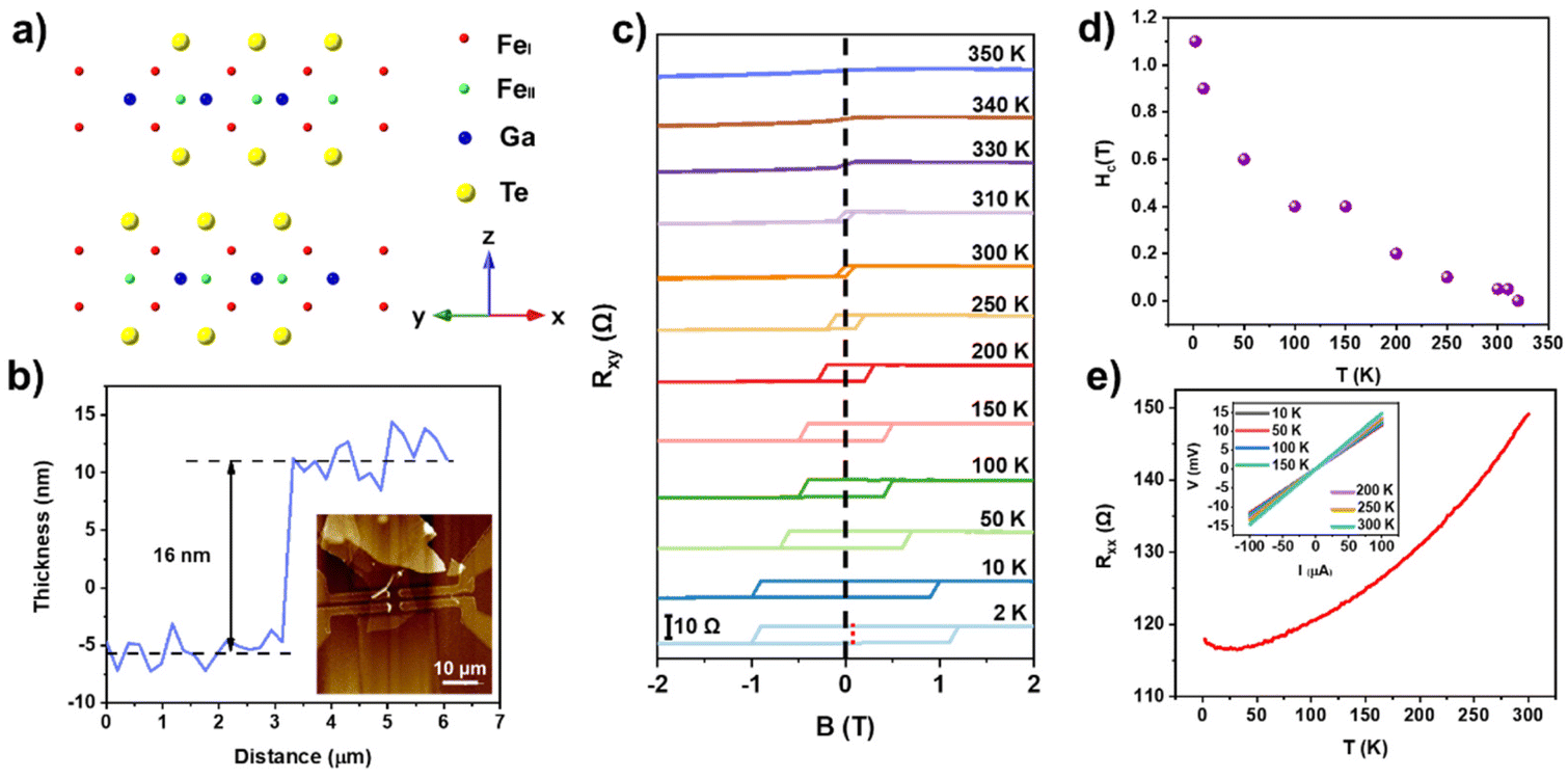 | ||
| Fig. 1 The crystal structure and magneto-transport characterization of the vdW layered Fe3GaTe2 single crystals. (a) The front view of the crystal structure of Fe3GaTe2. (b) The AFM height profile and topography (inset) of the Fe3GaTe2 Hall device. (c) Hall resistance (Rxy) at different temperatures from 2 K to 350 K. (d) The extracted coercivities as a function of temperature. (e) The temperature-dependence of longitudinal resistance (Rxx). Inset: I–V curves at different temperatures. | ||
The fabricated spin-valve device consisted of two FM electrodes (Fe3GaTe2) and a non-magnetic spacer layer (MoS2); the diagram of the structure is shown in Fig. 2a. MoS2 is a semiconductor with a tunable bandgap (1.8 eV in the monolayer and 1.2 eV in the bulk32–34), whereas its vertical conductivity is relatively poor due to the weak interlayer interaction,35 thus making it an appropriate spacer layer for spin-valve devices. To avoid damage and contamination of this layer during the deposition of the Cr/Au electrodes, we fabricated the metal electrodes first, and the following procedure was finished in an Ar-filled glove box. We applied a four-terminal setup to measure the magnetoresistance (MR) so that the contact resistance of the device was excluded. The magneto-transport measurements were carried out under a magnetic field directed perpendicular to the ab plane. To observe the spin-valve effect, the switching fields of the two FM electrodes should be different.36,37 The switching fields are decided by the coercivity of Fe3GaTe2, which depends on the geometry and thickness of Fe3GaTe2.38 Thus, we selected Fe3GaTe2 with different geometry and thickness as the FM metal layers. The AFM image and the thickness profile of the device are shown in Fig. S1 in ESI,† indicating that the top and bottom Fe3GaTe2 layers measured 16.8 nm and 9.5 nm, respectively, and the middle few-layer MoS2 had a thickness of 4.5 nm. In addition, the Raman spectra of the top and bottom Fe3GaTe2 layers, MoS2 and the heterojunction are shown in Fig. S2 in ESI,† indicating the successful formation of the multilayer heterojunction. Moreover, the Raman signals of MoS2 exhibited an in-plane vibration mode E12g (∼383 cm−1) and the out-of-plane A1g mode (∼406 cm−1); the difference between E12g and A1g was ∼23 cm−1, suggesting the presence of multilayer MoS2,39,40 which is consistent with the AFM tests. It is worth mentioning that no shift or split of the E12g and A1g modes of MoS2 was observed in the Raman spectra after the formation of the heterojunction, implying that no significant defects or strains were induced during the fabrication of the device. The all-2D vdW structure ensured no damage or degradation occurred in the 2D nonmagnetic spacer layer, which can be inevitably caused during 3D FM electrode deposition in traditional spin valves.41Fig. 2c displays a typical MR curve with 1 μA bias current at 300 K. The perpendicular magnetic field was applied to sweep between −0.05 T and 0.05 T (blue square), and the resistance increased abruptly at B = 50 Oe and continued until B = 200 Oe. As the applied magnetic field became larger, the resistance exhibited a sudden decrease. When sweeping backwards (red square), a similar sudden increase followed by a decrease was observed. The two distinct values of resistance corresponded with the magnetization switching of the two Fe3GaTe2 layers. To begin with, the magnetization direction of the two Fe3GaTe2 layers was parallel, corresponding to low resistance. While reversing the magnetization, the magnetization vector of the Fe3GaTe2 layer with small coercivity will turn over first, rendering the magnetization direction of the two Fe3GaTe2 layers antiparallel. The optical image of the device is shown in Fig. 2b; regions I, II and III are circled by white, green and orange dashed lines, respectively, representing the bottom Fe3GaTe2, MoS2, and top Fe3GaTe2 layers, respectively. According to Fig. 2b, the area of the heterojunction was estimated as 7.75 μm2, and thus, the resistance-area product (RA) was 10.25 kΩ μm2 at 300 K. The MR ratio was obtained according to the equation MR = (RAP − RP)/RP, where RAP and RP refer to the resistance of the antiparallel and parallel magnetic configurations of the two Fe3GaTe2 layers, respectively. According to the equation, the MR ratio of the Fe3GaTe2/MoS2/Fe3GaTe2 heterojunction was determined as 0.31% at 300 K (Fig. 2c) and 15.89% at 2.3 K (see data and discussion on Fig. 4a below). The MR at 10 K (11.97%) was approximately 30 times and 16 times that of the conventional spin valves NiFe/MoS2/NiFe (0.4%) and NiFe/Au/MoS2/NiFe (0.73),22 respectively, and 4 times that of the Fe3GeTe2/MoS2/Fe3GeTe2 (3.1%)24 spin valve. Moreover, when a reverse bias current was applied during MR measurement (Fig. 2d), the MR ratio showed little difference compared with that obtained from Fig. 2c, suggesting that the interface in the fabricated spin valve was symmetric.
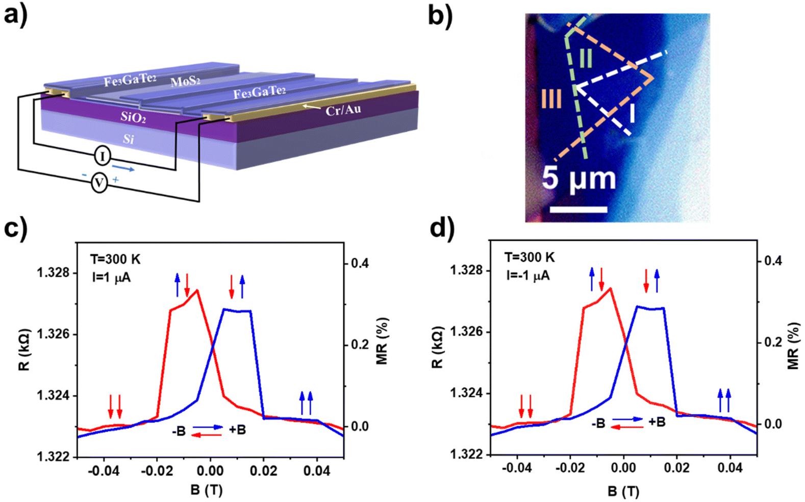 | ||
| Fig. 2 Spin-valve device characterization and magneto-transport properties. (a) The schematic of the Fe3GaTe2/MoS2/Fe3GaTe2 heterojunction spin-valve device. (b) The optical image of the device; regions I, II and III represent the bottom Fe3GaTe2, MoS2, and top Fe3GaTe2 layers, respectively. (c and d) Resistance and MR vs the perpendicular magnetic field at 300 K with a bias current of 1 μA and −1 μA. The arrows represent the magnetization alignment directions of Fe3GaTe2. | ||
The electrical characteristics were investigated next. Fig. 3a depicts the temperature-dependent resistance exhibiting an overall downward trend, indicating metallic behavior. The vertical heterojunction resistance was dominated by MoS2, which is a semiconductor, while the junction showed metallic behavior. This can be the result of the strong hybridization between the S atoms of MoS2 and the Te/Ga/Fe atoms.42 Notably, there was an increase as the temperature dipped below 50 K due to the Kondo effect. The linear current–voltage (I–V) curves at various temperatures in Fig. 3b suggest Ohmic contact between Fe3GaTe2 and MoS2. Besides, they also imply that no tunnel barrier was formed in the heterojunction, and MoS2 acted as a conducting layer that enables the two Fe3GaTe2 electrodes to be flipped independently under a magnetic field, which is critical to spin transport between the two FM layers. Fig. 3c shows the I–V curves tested in the parallel (IP) and antiparallel (IAP) magnetization modes at 2.3 K, where low and high resistances were obtained, corresponding to the MR-B test.
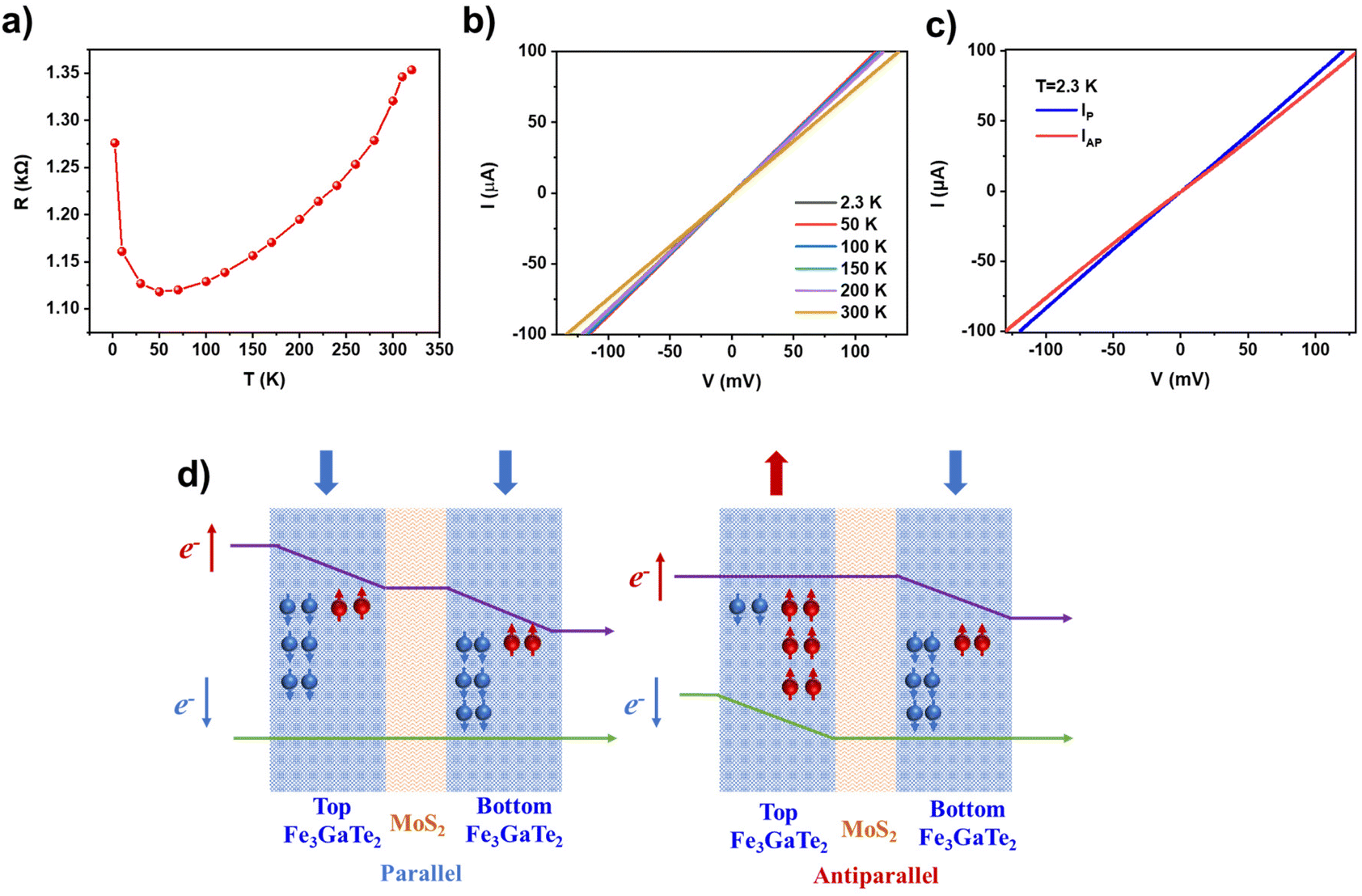 | ||
| Fig. 3 The electrical and magneto-transport properties of the Fe3GaTe2/MoS2/Fe3GaTe2 heterojunction spin-valve device. (a) Resistance vs. temperature of the spin-valve device. (b) I–V curves at different temperatures. (c) I–V curves measured at the parallel (IP) and antiparallel (IAP) magnetization configurations at 2.3 K. (d) The schematic of electron transport in the Fe3GaTe2/MoS2/Fe3GaTe2 heterojunction when the two Fe3GaTe2 electrodes are in the parallel and antiparallel configurations, respectively. | ||
To understand the physical mechanism of our spin-valve devices, the schematics of electron transport in the Fe3GaTe2/MoS2/Fe3GaTe2 heterojunctions are shown in Fig. 3d, where the purple and green lines represent the transport channels for the spin-up and -down electrons, respectively, while blue and red arrows indicate the magnetization directions of the Fe3GaTe2 electrodes. As the current flows through the heterojunction, it is proportional to the product of density of states (DOS) of the two Fe3GaTe2 electrodes.43,44 The junction resistances can be attributed to the difference in the DOS of the majority and minority spins, which is determined by the magnetization direction. To be specific, when the two Fe3GaTe2 electrodes are magnetized downward (in the parallel magnetic configuration, left panel of Fig. 3d), the spin-up electrons of the two electrodes are intensely scattered due to their low DOS, contributing to high spin-up channel resistance, while the scattering of the spin-down electrons is less as they can pass through the junction, and the spin-down channel resistance is relatively low, thus leading to low junction resistance (RP). When the top and bottom Fe3GaTe2 electrodes are magnetized upward and downward, respectively (in the antiparallel magnetic configuration, right of Fig. 3d), the spin-up and -down electrons are intensely scattered in the bottom and top Fe3GaTe2 layers, respectively. Thus, the resistances of both the spin-up and spin-down channels are high, producing high junction resistance (RAP).
To investigate the influence of the performing current on the performance of the spin valve, MR measurements at various bias currents were carried out at 2.3 K and 300 K, respectively. As shown in Fig. 4a and b, the spin-valve effect was observed at bias currents ranging from 10 nA to 30 μA, resulting in the maintenance of stable low working currents down to 10 nA (0.13 A cm−2) at both 2.3 K and 300 K. The current intensity could have been lower, but the test was limited by our physical property measurement system. This indicates that the spin valve can work as a low-power-consumption device at room temperature and has great potential in room-temperature spintronics. Notably, the MR curves measured at 2.3 K (Fig. 4a) were not symmetrical, implying that the coercivities of Fe3GaTe2 under negative and positive magnetic fields are different, which might be related to the pining of magnetization induced by defects.45 At higher temperatures, the pining was weakened, as shown in Fig. 4b.Moreover, multiple jumps were observed (Fig. 4a), which is caused by the reversal of magnetization at different parts of the junction due to the slightly different values of the magnetic field.46Fig. 4c and d demonstrate the current-dependent MR values extracted from Fig. 4a and b, respectively. At 2.3 K, when the bias current was smaller than 1 μA, the MR ratio was maintained at ∼15.5%, suggesting that the spin valve can work in a wide range of bias currents. As the applied bias current increased exponentially, the MR almost decreased linearly, which might be corresponding to high-energy electron scattering at the interface of Fe3GaTe2/MoS2.47 At 300 K, the MR ratio showed little dependence on the bias current, and we speculate that this is because the enhancement in thermal fluctuation diminishes electron scattering.47 To understand the influence of MoS2 thickness on the MR ratio of the spin valve, other devices with three different MoS2 thicknesses were fabricated, as shown in Fig. S4.† The three representative devices were tested at 2.3 K with 1 μA bias current, and the MR showed a spacer layer thickness-dependent behavior. When the MoS2 layer thickness was 8 nm, the MR was 2.4%. With an increase in the thickness of MoS2 to 10 nm, the MR dropped to 0.77% and finally down to 0.53% when the MoS2 thickness was 17 nm. MR decreased monotonically as the thickness increased, which could be further optimized by adjusting the thickness of the spacer.
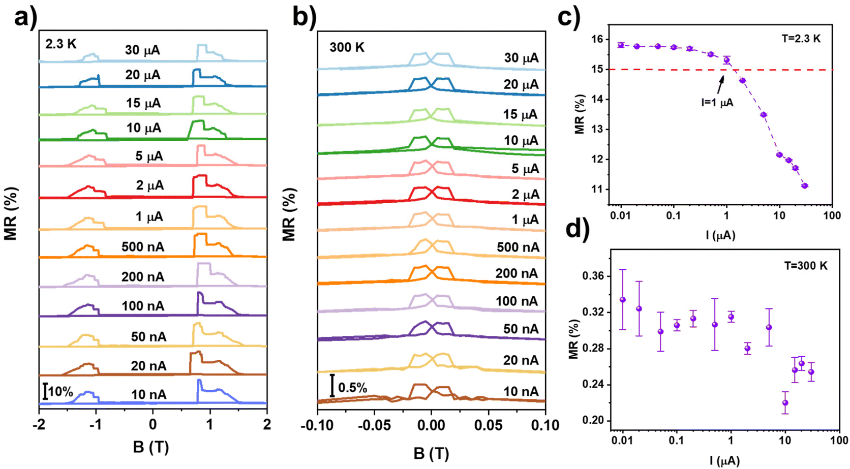 | ||
| Fig. 4 Bias-current-dependence of the spin-valve effect in the Fe3GaTe2/MoS2/Fe3GaTe2 device. MR curves measured at different bias currents from 10 nA to 30 μA at (a) 2.3 K and (b) 300 K. The extracted MR ratios as a function of the bias current at (c) 2.3 K and (d) 300 K. | ||
The temperature dependence of the spin valve was further studied by measuring the MR ratios at various temperatures up to 310 K. The MR ratios extracted from Fig. 5a are shown in Fig. 5b. The MR ratio monotonically decreased as the temperature increased and still retained its value at room temperature, corresponding to the TC of Fe3GaTe2. MR is closely dependent on spin polarization, which can be described as 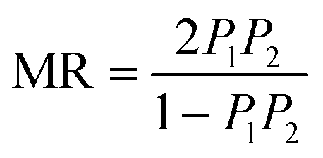 , according to the Julliere model,48 where P1 and P2 refer to the spin polarization values of the top and bottom FM layers. In our spin-valve device, the two FM layers were of the same material, so we set P1 ≈ P2 = P. Based on this, the relationship between the calculated P and temperature is depicted in Fig. 5c; the P value decreased from 27% to 4% as the temperature was increased from 2.3 K to 300 K, which is higher than that observed in other MoS2-based spin-valve devices. However, compared with heterojunctions that are based on the tunneling effect, such as Fe3GeTe2/InSe/Fe3GeTe2,49 Fe3GeTe2/BN/Fe3GeTe2,18 and Fe3GaTe2/WSe2/Fe3GaTe2,50 this value is still relatively low due to the spin-polarization loss in Fe3GaTe2 when the electrons cross through the MoS2 spacer, which can be further improved by replacing the spacer layer with wide-bandgap semiconductors or insulators. The temperature-dependence of P was fitted based on the Bloch law51 using the equation P(T) = P(0)(1 − αT3/2), where P(0) refers to the spin polarization at 0 K, and α is a material-dependent constant.52,53 The α of our spin valve was 1.6 × 10⁻⁴ K−3/2, which is larger than those of Co (1–6 × 10⁻⁶ K−3/2) and NiFe (3–5 × 10⁻⁵ K−3/2).54 Generally, α is larger for the surface compared with the bulk due to surface exchange softening.55,56 The larger α here may be the result of interface scattering.57
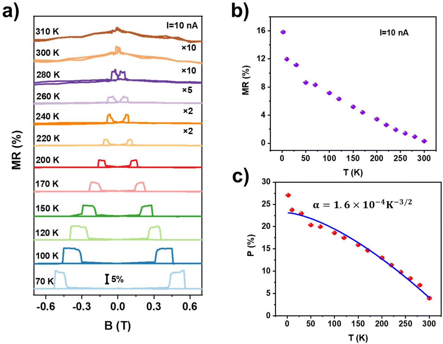 | ||
| Fig. 5 Temperature-dependence of the spin-valve effect in the Fe3GaTe2/MoS2/Fe3GaTe2 device. (a) MR curves measured at different temperatures from 70 K to 310 K with a fixed bias current of 10 nA. (b) The extracted MR ratios as a function of temperature. (c) Spin polarization as a function of temperature. The blue line is the fitting curve according to the Bloch law. | ||
3. Conclusion
We report a room-temperature, FM 2D crystal-based all-2D vdW spin-valve heterojunction device with a typical spin-valve effect, showing strong spacer (MoS2)-thickness-dependence in the vdW heterojunctions. The MR of the all-2D vdW spin valve device was 15.89% at 2.3 K and 11.97% at 10 K, which are 4–30 times the MR of the spin valves of Fe3GeTe2/MoS2/Fe3GeTe2 and conventional NiFe/MoS2/NiFe. Importantly, the spin-valve effect could be robustly maintained at 300 K with low working currents down to 10 nA (0.13 A cm−2). This work provides a general vdW platform for developing room temperature, 2D FM crystal-based 2D spin valve devices. Note that before submitting this work, we first published the results as preprint in arXiv.58 Some discussions can be referred between these two published versions. During the publication of this work, we also published our collaborated work using WSe2 as spacer50 and our another work using MoSe2 spacer.594. Experimental section
4.1. Device fabrication
4.2. Device tests
The thickness of the Fe3GaTe2 and MoS2 flakes were identified by atomic force microscopy (AFM, XE7, Park; SPM9700, Shimadzu; Dimension EDGE, Bruker). The Raman spectra were obtained using a Raman spectrometer (LabRAM HR800, Horiba Jobin–Yvon) with an excitation wavelength of 532 nm. The magneto-transport and electrical transport properties were measured in a physical property measurement system (PPMS, DynaCool, Quantum Design). The magnetic field was applied parallel to the c-axis of Fe3GaTe2. At each magnetic field or temperature sampling point, the resistance was measured 25 times to obtain an average in the constant current mode.Author contributions
H. C. designed the project. W. J. and G. Z. prepared the materials and fabricated the devices. W. J., H. W. and L. Y. did the crystal characterization and physical property measurements. H. C., W. Z. and W. J. analyzed the results. H. C. and W. J. wrote the paper. All authors discussed the results and commented on the manuscript.Conflicts of interest
The authors declare no conflict of interest.Acknowledgements
This work was supported by the National Key Research and Development Program of China (Grant No. 2022YFE0134600) and the National Natural Science Foundation of China (grant no. 52272152, 61674063 and 62074061), the Foundation of Shenzhen Science and Technology Innovation Committee (grant no. JCYJ20210324142010030 and JCYJ20180504170444967), and the fellowship of China Postdoctoral Science Foundation (grant no. 2022M711234). We thank the AFM and Raman tests from Analytical Center of Huazhong University of Science and Technology.References
- M. A. Khan, J. Sun, B. Li, A. Przybysz and J. Kosel, Eng. Res. Express, 2021, 3, 022005 CrossRef.
- J.-G. Zhu and C. Park, Mater. Today, 2006, 9, 36 CrossRef CAS.
- C. Ren, Q. Bayin, S. Feng, Y. Fu, X. Ma and J. Guo, Biosens. Bioelectron., 2020, 165, 112340 CrossRef CAS.
- B. Behin-Aein, D. Datta, S. Salahuddin and S. Datta, Nat. Nanotechnol., 2010, 5, 266 CrossRef CAS PubMed.
- B. Dieny and I. L. Prejbeanu, Introduction to Magnetic Random–Access Memory, 2017, p. 101 Search PubMed.
- W.-H. Hsu and R. H. Victora, Appl. Phys. Lett., 2021, 118, 072406 CrossRef CAS.
- T. Nakatani, Z. Gao and K. Hono, MRS Bull., 2018, 43, 106 CrossRef CAS.
- K. Dolui, A. Narayan, I. Rungger and S. Sanvito, Phys. Rev. B: Condens. Matter Mater. Phys., 2014, 90, 041401 CrossRef CAS.
- M. Z. Iqbal, M. W. Iqbal, J. H. Lee, Y. S. Kim, S.-H. Chun and J. Eom, Nano Res., 2013, 6, 373 CrossRef CAS.
- J. Meng, J.-J. Chen, Y. Yan, D.-P. Yu and Z.-M. Liao, Nanoscale, 2013, 5, 8894 RSC.
- R. B. Morgunov, G. L. L'Vova, A. D. Talantsev, Y. Lu, X. Devaux, S. Migot, O. V. Koplak, O. S. Dmitriev and S. Mangin, Thin Solid Films, 2017, 640, 8 CrossRef CAS.
- S. Zhang, H. Wu, L. Yang, G. Zhang, Y. Xie, L. Zhang, W. Zhang and H. Chang, Mater. Horizons, 2022, 9, 559 RSC.
- Z. Guo, R. Cao, H. Wang, X. Zhang, F. Meng, X. Chen, S. Gao, D. K. Sang, T. H. Nguyen, A. T. Duong, J. Zhao, Y. J. Zeng, S. Cho, B. Zhao, P. H. Tan, H. Zhang and D. Fan, Natl. Sci. Rev., 2021, 9(5), nwab098 CrossRef PubMed.
- L. Gao, C. Ma, S. Wei, A. V. Kuklin, H. Zhang and H. Ågren, ACS Nano, 2021, 15(1), 954–965 CrossRef CAS PubMed.
- Y. Zhang, P. Huang, J. Guo, R. Shi, W. Huang, Z. Shi, L. Wu, F. Zhang, L. Gao, C. Li, X. Zhang, J. Xu and H. Zhang, Adv. Mater., 2020, 32, 2001082 CrossRef CAS PubMed.
- H. Qiao, Z. Huang, X. Ren, S. Liu, Y. Zhang, X. Qi and H. Zhang, Adv. Opt. Mater., 2020, 8, 1900765 CrossRef CAS.
- T. Fan, Z. Xie, W. Huang, Z. Li and H. Zhang, Nanotechnology, 2019, 30, 114002 CrossRef CAS PubMed.
- Z. Wang, D. Sapkota, T. Taniguchi, K. Watanabe, D. Mandrus and A. F. Morpurgo, Nano Lett., 2018, 18, 4303–4308 CrossRef CAS PubMed.
- S. Albarakati, C. Tan, Z. Chen, J. G. Partridge, G. Zheng, L. Farrar, E. L. H. Mayes, M. R. Field, C. Lee, Y. Wang, Y. Xiong, M. Tian, F. Xiang, A. R. Hamilton, O. A. Tretiakov, D. Culcer, Y. Zhao and L. Wang, Sci. Adv., 2019, 5, eaaw0409 CrossRef CAS PubMed.
- K. F. Mak, C. Lee, J. Hone, J. Shan and T. F. Heinz, Phys. Rev. Lett., 2010, 105, 136805 CrossRef PubMed.
- Z. Y. Zhu, Y. C. Cheng and U. Schwingenschlögl, Phys. Rev. B: Condens. Matter Mater. Phys., 2011, 84, 153402 CrossRef.
- W. Wang, A. Narayan, L. Tang, K. Dolui, Y. Liu, X. Yuan, Y. Jin, Y. Wu, I. Rungger, S. Sanvito and F. Xiu, Nano Lett., 2015, 15, 5261 CrossRef CAS.
- K. Zhao, Y. Xing, J. Han, J. Feng, W. Shi, B. Zhang and Z. Zeng, J. Magn. Magn. Mater., 2017, 432, 10 CrossRef CAS.
- H. Lin, F. Yan, C. Hu, Q. Lv, W. Zhu, Z. Wang, Z. Wei, K. Chang and K. Wang, ACS Appl. Mater. Interfaces, 2020, 12, 43921 CrossRef CAS PubMed.
- Y. Zheng, X. Ma, F. Yan, H. Lin, W. Zhu, Y. Ji, R. Wang and K. Wang, npj 2D Mater. Appl., 2022, 6, 62 CrossRef CAS.
- N. D. Mermin and H. Wagner, Phys. Rev. Lett., 1966, 17, 1133 CrossRef CAS.
- C. Gong, L. Li, Z. Li, H. Ji, A. Stern, Y. Xia, T. Cao, W. Bao, C. Wang, Y. Wang, Z. Q. Qiu, R. J. Cava, S. G. Louie, J. Xia and X. Zhang, Nature, 2017, 546, 265 CrossRef CAS PubMed.
- B. Huang, G. Clark, E. Navarro-Moratalla, D. R. Klein, R. Cheng, K. L. Seyler, D. Zhong, E. Schmidgall, M. A. McGuire, D. H. Cobden, W. Yao, D. Xiao, P. Jarillo-Herrero and X. Xu, Nature, 2017, 546, 270 CrossRef CAS PubMed.
- Y. Deng, Y. Yu, Y. Song, J. Zhang, N. Z. Wang, Z. Sun, Y. Yi, Y. Z. Wu, S. Wu, J. Zhu, J. Wang, X. H. Chen and Y. Zhang, Nature, 2018, 563, 94 CrossRef CAS PubMed.
- G. Zhang, F. Guo, H. Wu, X. Wen, L. Yang, W. Jin, W. Zhang and H. Chang, Nat. Commun., 2022, 13, 5067 CrossRef CAS.
- T. Zhang, Y. Zhang, M. Huang, B. Li, Y. Sun, Z. Qu, X. Duan, C. Jiang and S. Yang, Adv. Sci., 2022, 9, 2105483 CrossRef CAS PubMed.
- B. Radisavljevic and A. Kis, Nat. Mater., 2013, 12, 815 CrossRef CAS.
- S. Chuang, C. Battaglia, A. Azcatl, S. McDonnell, J. S. Kang, X. Yin, M. Tosun, R. Kapadia, H. Fang, R. M. Wallace and A. Javey, Nano Lett., 2014, 14, 1337 CrossRef CAS.
- K. F. Mak, C. Lee, J. Hone, J. Shan and T. F. Heinz, Phys. Rev. Lett., 2010, 105, 136805 CrossRef PubMed.
- M. Xu, T. Liang, M. Shi and H. Chen, Chem. Rev., 2013, 113, 3766 CrossRef CAS.
- I. Žutić, J. Fabian and S. Das Sarma, Rev. Mod. Phys., 2004, 76, 323 CrossRef.
- J. M. D. Coey, Magnetism and Magnetic Materials, Cambridge University Press, Cambridge, 2010 Search PubMed.
- C. Tan, J. Lee, S.-G. Jung, T. Park, S. Albarakati, J. Partridge, M. R. Field, D. G. McCulloch, L. Wang and C. Lee, Nat. Commun., 2018, 9, 1554 CrossRef.
- H. Li, Q. Zhang, C. C. R. Yap, B. K. Tay, T. H. T. Edwin, A. Olivier and D. Baillargeat, Adv. Funct. Mater., 2012, 22, 1385 CrossRef CAS.
- C. Lee, H. Yan, L. E. Brus, T. F. Heinz, J. Hone and S. Ryu, ACS Nano, 2010, 4, 2695 CrossRef CAS.
- W. Zhang, P. K. J. Wong, X. Zhou, A. Rath, Z. Huang, H. Wang, S. A. Morton, J. Yuan, L. Zhang, R. Chua, S. Zeng, E. Liu, F. Xu, Ariando, D. H. C. Chua, Y. P. Feng, G. van der Laan, S. J. Pennycook, Y. Zhai and A. T. S. Wee, ACS Nano, 2019, 13, 2253 CAS.
- K. Dolui, A. Narayan, I. Rungger and S. Sanvito, Phys. Rev. B: Condens. Matter Mater. Phys., 2014, 90, 041401 CrossRef CAS.
- M. Bowen, V. Cros, F. Petroff, A. Fert, C. Martínez Boubeta, J. L. Costa-Krämer, J. V. Anguita, A. Cebollada, F. Briones, J. M. de Teresa, L. Morellón, M. R. Ibarra, F. Güell, F. Peiró and A. Cornet, Appl. Phys. Lett., 2001, 79, 1655 CrossRef CAS.
- T. Miyazaki and N. Tezuka, J. Magn. Magn. Mater., 1995, 139, L231–L234 CrossRef CAS.
- J. Dho, E. K. Lee, J. Y. Park and N. H. Hur, J. Magn. Magn. Mater., 2005, 285, 164 CrossRef CAS.
- Z. Wang, D. Sapkota, T. Taniguchi, K. Watanabe, D. Mandrus and A. F. Morpurgo, Nano Lett., 2018, 18, 4303–4308 CrossRef CAS PubMed.
- J. Zhang and R. M. White, J. Appl. Phys., 1998, 83, 6512 CrossRef CAS.
- M. Julliere, Phys. Lett. A, 1975, 54, 225 CrossRef.
- W. Zhu, H. Lin, F. Yan, C. Hu, Z. Wang, L. Zhao, Y. Deng, Z. R. Kudrynskyi, T. Zhou, Z. D. Kovalyuk, Y. Zheng, A. Patanè, I. Žutić, S. Li, H. Zheng and K. Wang, Adv. Mater., 2021, 33, 2104658 CrossRef CAS.
- W. Zhu, S. Xie, H. Lin, G. Zhang, H. Wu, T. I. Hu, Z. Wang, X. Zhang, J. Xu, Y. Wang, Y. Zheng, F. Yan, J. Zhang, L. Zhao, A. Patanè, J. Zhang, H. Chang and K. Wang, Chin. Phys. Lett., 2022, 39, 128501 CrossRef.
- R. Sharif, S. Shamaila, F. Shaheen, J. Y. Chen, M. Khaleeq-ur-Rahman and K. Hussain, Appl. Phys. Lett., 2013, 102, 013114 CrossRef.
- C. H. Shang, J. Nowak, R. Jansen and J. S. Moodera, Phys. Rev. B: Condens. Matter Mater. Phys., 1998, 58, R2917 CrossRef CAS.
- J. Mathon and S. B. Ahmad, Phys. Rev. B: Condens. Matter Mater. Phys., 1988, 37, 660 CrossRef PubMed.
- C. H. Shang, J. Nowak, R. Jansen and J. S. Moodera, Phys. Rev. B: Condens. Matter Mater. Phys., 1998, 58, R2917 CrossRef CAS.
- D. L. Mills and A. A. Maradudin, J. Phys. Chem. Solids, 1967, 28, 1855 CrossRef CAS.
- J. Mathon and S. B. Ahmad, Phys. Rev. B: Condens. Matter Mater. Phys., 1988, 37, 660 CrossRef.
- J. Unguris, D. T. Pierce and R. J. Celotta, Phys. Rev. B: Condens. Matter Mater. Phys., 1984, 29, 1381 CrossRef CAS.
- W. Jin, G. Zhang, H. Wu, L. Yang, W. Zhang and H. Chang, arXiv, 2022, preprint, arXiv:2211.06165 DOI:10.48550/arXiv.2211.06165.
- H. Yin, P. Zhang, W. Jin, B. Di, H. Wu, G. Zhang, W. Zhang and H. Chang, CrystEngComm, 2023 10.1039/d2ce01695h.
Footnote |
| † Electronic supplementary information (ESI) available. See DOI: https://doi.org/10.1039/d2nr06886a |
| This journal is © The Royal Society of Chemistry 2023 |