
 Open Access Article
 This Open Access Article is licensed under a Creative Commons Attribution-Non Commercial 3.0 Unported Licence
Ferroelectric Hf0.5Zr0.5O2 films with improved endurance obtained through low temperature epitaxial growth on seed layers†
Tingfeng
Song
a,
Romain
Bachelet
 b,
Guillaume
Saint-Girons
b,
Ignasi
Fina
*a and
Florencio
Sánchez
*a
b,
Guillaume
Saint-Girons
b,
Ignasi
Fina
*a and
Florencio
Sánchez
*a
aInstitut de Ciència de Materials de Barcelona (ICMAB-CSIC), Campus UAB, Bellaterra 08193, Barcelona, Spain. E-mail: ifina@icmab.es; fsanchez@icmab.es
bUniv. Lyon, Ecole Centrale de Lyon, INSA Lyon, Université Claude Bernard Lyon 1, CPE Lyon, CNRS, Institut des Nanotechnologies de Lyon - INL, UMR5270, 69134 Ecully, France
First published on 2nd February 2023
Abstract
Crystallization temperature is a critical parameter in the stabilization of the metastable ferroelectric phase of HfO2. The optimal crystallization temperature used for polycrystalline films is too low to grow epitaxial films. We have developed a new growth strategy, based on the use of an ultrathin seed layer, to obtain high-quality epitaxial films of orthorhombic Hf0.5Zr0.5O2 at a lower temperature. The threshold temperature for epitaxy is reduced from about 750 °C to about 550 °C using a seed layer. Epitaxial films deposited at low temperatures exhibit highly enhanced endurance, and films grown at 550–600 °C show high polarization, no wake-up effect, and greatly reduced fatigue and improved endurance in comparison with the films deposited at high temperatures without a seed layer. We propose that the endurance enhancement is due to a positive effect of the defects, which limits the propagation of pinned ferroelectric domains.
1. Introduction
HfO2 films can exhibit robust ferroelectricity at room temperature, and their compatibility with CMOS processes opens up new possibilities for memory and other ferroelectric-based devices.1–3 Bulk HfO2 under ambient conditions is monoclinic and paraelectric. Ferroelectricity arises in a metastable orthorhombic phase stabilized in HfO2 nanometric films, typically doped, and prepared under particular conditions. Different chemical elements (Si, Al, Sr, Y, Zr, etc.) have been used as dopant atoms, with Hf0.5Zr0.5O2 (HZO) being the most investigated composition. In the commonly investigated polycrystalline films, the orthorhombic phase is formed by thermal annealing. Annealing at excessively high temperatures4,5 or for an excessively long time6 promotes the formation of the stable monoclinic phase. It is proposed that the stabilization of the metastable ferroelectric phase is due to a combined effect of the surface energy contribution and kinetic limitations.7 Before annealing, the quasi-amorphous films would have small orthorhombic nuclei. During annealing, the nanocrystals transform into a tetragonal phase that is stable at high temperatures. However, when the crystal grains increase in size, the lowest energy corresponds to the monoclinic phase. However, the energy barrier for this phase transformation is high, and the transformation is kinetically suppressed if annealing is short and at a moderate temperature. It has also been reported that the monoclinic phase can be transformed into tetragonal and orthorhombic phases by very high temperature annealing (1000–1200 °C) in solid phase epitaxy of Y-doped HfO2 films.8 Therefore, in the crystallization of quasi-amorphous films, the annealing temperature is a critical parameter to stabilize the metastable orthorhombic phase rather than the thermodynamically stable monoclinic phase.Epitaxial growth from a vapor phase radically differs from crystallization processes by annealing. Diffusion of atoms on a surface and chemical bonding at specific positions generally require a high thermal energy, suitable saturation conditions, and a growth rate low enough to limit crystalline defects. In particular, the ferroelectric phase of doped HfO2 has been stabilized in epitaxial films, mainly by pulsed laser deposition, and with a substrate temperature of around 700–800 °C.9–13 The study of the window for epitaxial growth of ferroelectric HZO films revealed a severe reduction in crystallinity for temperatures (substrate heater block) below around 700 °C.14 The possibility of epitaxial growth at a lower temperature would be desirable due to its impact on the microstructure of the film. Epitaxial films of ferroelectric HfO2 generally present a mixture of phases and crystal variants. Microstructure, including the polymorph ratio, crystal grain size and defects, can be critical for the ferroelectric properties of HfO2. However, the high thermal energy required for epitaxy precludes investigation of low-temperature conditions that could influence the stabilization of the orthorhombic phase and tailor the microstructure of the films.
In heteroepitaxial growth, interface energy is an important factor for the formation of crystal nuclei and for the determination of the crystal polymorphs that nucleate. We have investigated a new strategy to grow ferroelectric HfO2 films, with the aim of widening the window for epitaxial growth at a lower temperature. Films were grown in two steps. In the first step, an ultra-thin seed layer is grown at the optimal high temperature (800 °C) for the heteroepitaxial growth of HZO.10–14 The HZO growth then continues (second step) at a lower temperature on the epitaxial HZO seed layer. Homoepitaxial growth is expected to be possible at a lower temperature, since there is no HZO film/HZO seed layer interface energy contribution, in contrast with the high interface energy at the HZO seed layer/substrate interface. We will show that the use of the seed layer allows the stabilization of the orthorhombic phase at a lower temperature. The films grown at low temperatures (550–600 °C) show excellent ferroelectric properties: slightly reduced ferroelectric polarization, the absence of wake-up effect and greatly enhanced robustness against fatigue.
2. Experimental
Top ferroelectric HZO films and bottom La0.67Sr0.33MnO3 (LSMO) electrodes were grown on (001)-oriented SrTiO3 (STO) substrates in a single process by pulsed laser deposition (PLD) using a KrF excimer laser (248 nm wavelength). The LSMO electrodes, thickness t ∼ 25 nm, were grown at TS = 700 °C and oxygen pressure PO2 = 0.1 mbar. The HZO films were then grown in two steps. First, an ultra-thin (t ∼ 2.2 nm) HZO seed layer was grown at 800 °C and 0.1 mbar of oxygen with 200 laser pulses at a growth rate of 0.11 Å per laser pulse. Next, the seed layer was cooled under 0.1 mbar of oxygen to a temperature TS in the 550–750 °C range, and an HZO film (t ∼ 6.6 nm) was grown with 600 laser pulses at that temperature and the same oxygen pressure and growth rate as those of the seed layer. Another film was grown at 800 °C, in a two-step process with a dwell time of 18 min after deposition of the first 2.2 nm. At the end of the deposition, samples were cooled under 0.2 mbar of oxygen partial pressure. Another series of films was deposited at 650, 700 and 750 °C on Si(001) buffered with an epitaxial STO layer. Details on the STO growth conditions and structural properties are reported elsewhere.15,16Structural characterization of the HZO films was performed by X-ray diffraction (XRD) using Cu Kα radiation. Platinum top electrodes, 20 nm thick and 20 μm in diameter, were grown by dc magnetron sputtering through stencil masks for electrical characterization. Ferroelectric polarization loops were measured at 1 kHz using the dynamic leakage current compensation (DLCC) procedure at room temperature in the top-bottom configuration with the bottom electrode being grounded.17,18 Endurance was measured by cycling the sample at 100 kHz using bipolar square pulses of amplitude 4.5 V and measuring polarization loops at 1 kHz.
3. Results
Fig. 1a shows XRD θ–2θ scans of the HZO films on STO substrates. The growth temperature (second step) is indicated on the right. The high intensity peaks at 2θ around 23 and 47° correspond to the (001) and (002) reflections from the STO substrate. The corresponding reflections from the LSMO electrode lie to the right of the substrate peaks. Furthermore, all samples exhibit a peak at 2θ around 30°, the position of the (111) reflection of the orthorhombic (o) phase of HZO. Therefore, HZO crystallizes over the entire investigated TS range. The peak is broad, as expected considering that the HZO total thickness is less than 9 nm. Epitaxial stabilization of the ferroelectric phase of HZO on LSMO electrodes usually requires a deposition temperature above around 700 °C.10–14,19 Pole figures (Fig. 1c) and ϕ-scans (Fig. 1c) around asymmetrical o-HZO(−111) reflections confirm that the film grows epitaxially, even at TS = 550 °C (pole figures of the TS = 650 °C and 800 °C samples are provided in ESI S1†). The films show the epitaxial relationship and four sets of crystal variants usually observed in the epitaxial growth on LSMO(001).10 The right panel in Fig. 1a shows a 2θ zoomed region around the o-HZO(111) reflection, measured with a longer acquisition time. The o-HZO(111) reflection from all the films is accompanied by Laue fringes, more pronounced in the films deposited at a higher temperature, indicating a better crystalline quality and flatter interfaces.20,21 XRD measurements with a 2D detector are shown in ESI S2.† The o-HZO(111) reflection is a bright spot in all the samples, without broadening along the χ angle. There is an additional Bragg spot at around 2θ = 28.5° in the TS = 550 °C film. The 2θ position and the elongation along χindicate that it corresponds to the monoclinic (m)HZO(−111) reflection.10,14 The m-HZO(−111) spot decreases in intensity with increasing TS, and it is not detected in the films deposited at TS higher than 650 °C. In the films deposited at the highest TS, 750 and 800 °C, the sharp spot at a close position is a Laue fringe of the o-HZO(111) reflection. The total thickness of the HZO stack (seed layer and film) in each sample was determined by simulation of the o-HZO(111) reflection and the Laue fringes (ESI S3†). The total HZO thickness in the series of samples ranges from 8.3 to 8.9 nm, in agreement with the expected HZO growth rate of 0.11 Å per laser pulse. In Fig. 1, a tiny peak around 34.5° is also barely observed, corresponding to the position of the HZO{002} reflections of the monoclinic (m) phase. The peak, of a very low intensity, is observed only in some films, without correlation with TS. In contrast, the position of the o-HZO(111) peak varies monotonically with the deposition temperature. The dashed vertical line marks the position of the peak for the TS = 800 °C sample. It can be seen that as TS decreases, the peak shifts to a lower angle, indicating that the HZO(111) out-of-plane lattice distance, d(111), increases. To demonstrate that a seed layer is also effective for low-temperature epitaxy on Si(001) substrates, we used epitaxial STO buffer layers, which allow epitaxial growth of LSMO electrodes and HZO ferroelectric films.15 The XRD θ–2θ scans of the three films grown at 550, 600 and 650 °C (ESI S4†) confirm stabilization of the orthorhombic phase at a low TS, with a similar d(111) – TS dependence to the films on STO(001). | ||
| Fig. 1 (a) XRD θ–2θ scans of HZO films deposited on STO(001) at the temperature indicated on the right. Scans are shifted vertically for clarity. The enlarged 2θ region shown in the right panel was scanned with a longer acquisition time. The dashed vertical line marks the position of the peak in the TS = 800 °C sample. (b) Pole figures and (c) ϕ-scans around the o-HZO(−111) and STO(111) reflections of the TS = 550 °C sample. | ||
The intensity of the o-HZO(111) diffraction peak can be used as an approximation to estimate the orthorhombic phase content in the films. Fig. 2(a) shows the intensity of the o-HZO(111) peak, normalized to the LSMO(002) peak to compensate for the potential differences in the XRD measurement conditions of the samples, of films grown on seed layers on STO (red triangles) and Si (blue circles) substrates. The normalized intensity of the films on STO decreases with lowering the TS to 700 °C and shows less dependence for TS between 700 and 550 °C. The intensity–TS dependence is similar in the three samples on Si, although the normalized intensity is lower. The graph also includes the corresponding normalized intensity of films deposited at various TS directly on the LSMO/STO(001) electrode, without a seed layer (black squares), and having the same total thickness (∼8.8 nm).14 The TS = 800 °C sample with a seed layer has a slightly higher normalized intensity than that of the corresponding film without a seed layer, which could be due to the 18 min dwell time. The intensity of the films grown without a seed layer decreases very sharply with TS and is very low for TS below 750 °C. Fig. 2(a) indicates that (i) the growth of highly crystalline films below 750 °C is only achieved on seed layers and (ii) for higher temperatures, the use of a seed layer enhances HZO crystallization.
 | ||
| Fig. 2 Intensity of the o-(111) reflection, normalized to that of the LSMO(002) peak (a), and out-of-plane lattice distance corresponding to the o-(111) reflection (b), as a function of the deposition temperature TS for films on STO(001) (red triangles) and Si(001) (blue circles). Black squares represent data corresponding to the films on STO(001) deposited without a seed layer.35 | ||
The variation of the position of the o-HZO(111) peak with TS (Fig. 1) is quantified in Fig. 2(b). The lattice parameter d(111) increases monotonically with decreasing TS (red triangles) to about 1.3% and matches that of films grown at the same temperature without a seed layer (black squares). HZO(111) on highly mismatched LSMO(001) grows by the domain matching epitaxy mechanism,22 which results in null or very small epitaxial strain.23 However, the unit cell expansion of a film grown by PLD can be caused by defects that form when the energy of the PLD plasma is high.24–26 The energy of the atomic species in the PLD plasma reaching the substrate depends on the laser fluence, the target–substrate distance and the gas pressure.27–29 These parameters were kept constant in the preparation of the films discussed here. However, the number of defects that form in a film depends on the balance between the growth kinetics and thermodynamics.30 This balance, as demonstrated recently in the epitaxial growth of BaTiO3 films, can be tailored using the substrate temperature.31 The damage caused by the energetic PLD plasma is reduced by the high thermal energy in HZO films grown at high TS, while upon lowering the TS, the thermal energy is reduced, leading to more defects and d(111) expansion. The films on Si show the same dependence of d(111) on TS, but with a reduced value compared to the equivalent films on STO, which is a consequence of the tensile stress caused by the mismatch between the thermal expansion coefficients (TEC) of HZO and Si. Although TEC mismatch effects are less relevant if TS is lower, the two lineal dependences are parallel, probably because the seed layer is grown in all samples at TS = 800 °C.
All films are ferroelectric, confirming the stabilization of the orthorhombic phase throughout the TS range. The polarization loops of the films on STO(001) (Fig. 3(a), with the corresponding current–voltage loops in ESI S5†) are shifted towards negative voltage values. The positive coercive voltage VC+ increases with TS from around 1.8 V to 2.4 V, while the negative coercive voltage VC− ranges from −2.7 V to −3.0 V. It can be observed that all the loops are shifted towards the left between 0.40 and 0.87 V. This indicates that in all samples the imprint electric field is towards the LSMO electrode. The average coercive voltage VC = (VC+ + |VC−|)/2 is in the range of 2.2–2.7 V, increasing with TS (Fig. 3b, red triangles), corresponding to the coercive electric field EC in the 2.5–3.1 MV cm−1 range. The coercive voltage of the three films grown on the Si substrate is slightly lower and shows a similar TS dependence (blue circles). Epitaxial films grown directly on LSMO/STO(001) without a seed layer exhibit similar VC values and TS dependence (black squares). A high EC of about 2.5–3 MV cm−1, which exceeds the usual EC of polycrystalline films, is common in HZO epitaxial films of similar thickness.12,14 The remanent polarization is plotted against TS in Fig. 3(c) (red triangles). Pr decreases moderately with decreasing growth temperature, from 21.2 μC cm−2 in the TS = 800 °C film to 14 μC cm−2 in the TS = 550 °C film. A similar trend is observed if Pr values are obtained from PUND measurements (ESI S7†). The remanent polarization of the films on Si (polarization loops shown in ESI S6†) is comparable (blue circles). The polarization values of the films on STO(001) and Si(001) are similar to those of other epitaxial HZO films with the same thickness of these substrates.12 In the films deposited without a seed layer, the polarization is similar to that of the film deposited at 800 °C, 19.6 μC cm−2, but decreases sharply with TS to around 14 μC cm−2 in the TS = 650 °C film. The improved Pr in films deposited at increased TS is likely due to the larger amount of orthorhombic phase. The out-of-plane parameter also varies with TS (Fig. 2b), but previous studies of films grown on different oxide substrates23 and the much smaller lattice parameter of the films on Si suggest that there is no strong effect of strain on the ferroelectric polarization.
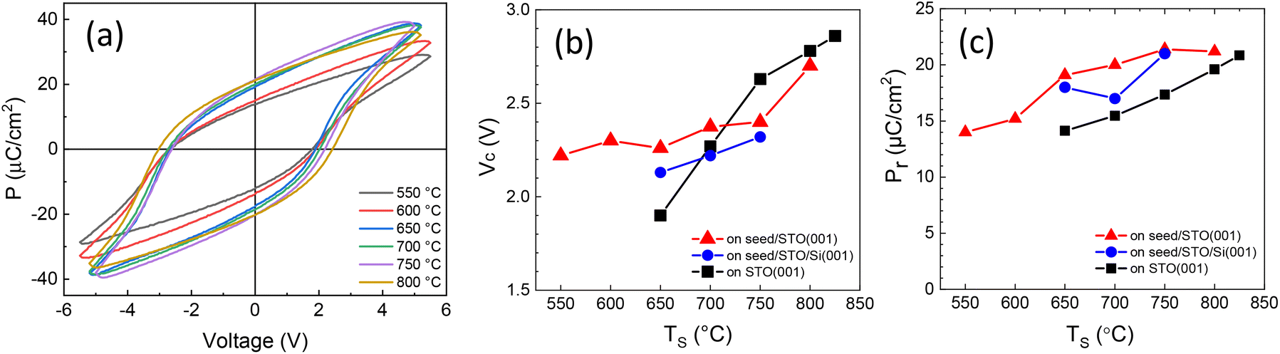 | ||
| Fig. 3 (a) Ferroelectric polarization loops of HZO films deposited at the temperature indicated at the bottom right. Coercive voltage (b) and remanent polarization (c), as a function of the deposition temperature TS for films on STO(001) (red triangles) and Si(001) (blue circles). Black squares represent data corresponding to the films on STO(001) deposited without a seed layer.35 | ||
Fatigue was investigated by cycling the capacitors with bipolar rectangular pulses of frequency 100 kHz and amplitude 4.5 V, close to the voltage used to obtain saturated loops (Fig. 3(a)). Endurance measurements are shown in Fig. 4(a–f) (see ESI S8† for polarization loops). There is no wake-up effect in these epitaxial capacitors. The wake-up effect is usually pronounced in polycrystalline films, and it is proposed to be caused by oxygen vacancies redistribution or electric-field induced phase transformations.2,32 Epitaxial films of doped HfO2 typically are wake-up free or have a very low wake-up effect10,33,34 which can be due to the lower amount of defects in epitaxial films. The TS = 550 °C film (Fig. 4(a)) has a moderately low 2Pr of 13.1 μC cm−2 in the pristine state, and there is no significant fatigue over 105 cycles (2Pr = 12.5 μC cm−2). 2Pr drops to 9.5 μC cm−2 after 107 cycles, and after 109 it is only 2.7 μC cm−2. More cycles caused an electric breakdown. HZO films grown at higher temperatures show fatigue from the beginning, the greater the higher TS. In the TS = 600 °C sample (Fig. 4(b)) the decrease in 2Pr after 105 cycles is low, decreasing from 16.2 to 12.9 μC cm−2. Thereafter, fatigue is more pronounced and 2Pr is 2.9 μC cm−2 after 109 cycles, before breakdown occurs. In the TS = 650 and 700 °C samples (Fig. 4(c and d), respectively), 2Pr in the pristine state is greater than 20 μC cm−2, but high fatigue begins after fewer cycles and, moreover, breakdown occurs earlier, after 4 × 10⁷ cycles. In the samples grown at the highest temperatures, 750 and 800 °C (Fig. 4(e and f), respectively), with a high initial 2Pr of more than 30 μC cm−2, the degradation of polarization is more evident, and the tendency of early breakdown with increased TS is confirmed, occurring after 107 cycles in both films. Therefore, the films deposited at low temperatures, although they have lower polarization in the pristine state, are less affected by fatigue and more robust against breakdown. The polarization is normalized in Fig. 4(g) to compare the endurance of the films grown at various TS on a seed layer (solid symbols and solid lines). The robustness against fatigue and electrical breakdown at low TS is evident. The graph also includes data of the films grown at various TS without a seed layer (empty symbols and dashed lines).35 The films deposited at a low TS without a seed layer already showed less fatigue. However, the crystallization and ferroelectric polarization of films deposited at less than 700 °C were too low. The use of a seed layer, which enhances crystallization, allows for epitaxial growth and high polarization at a lower temperature, with a positive impact on fatigue and resistance against breakdown as shown in Fig. 4(g). Moreover, all films in the series show excellent retention, with extrapolated remanent polarization after 10 years above 47% of the initial value for either positive or negative poling (ESI S9†).
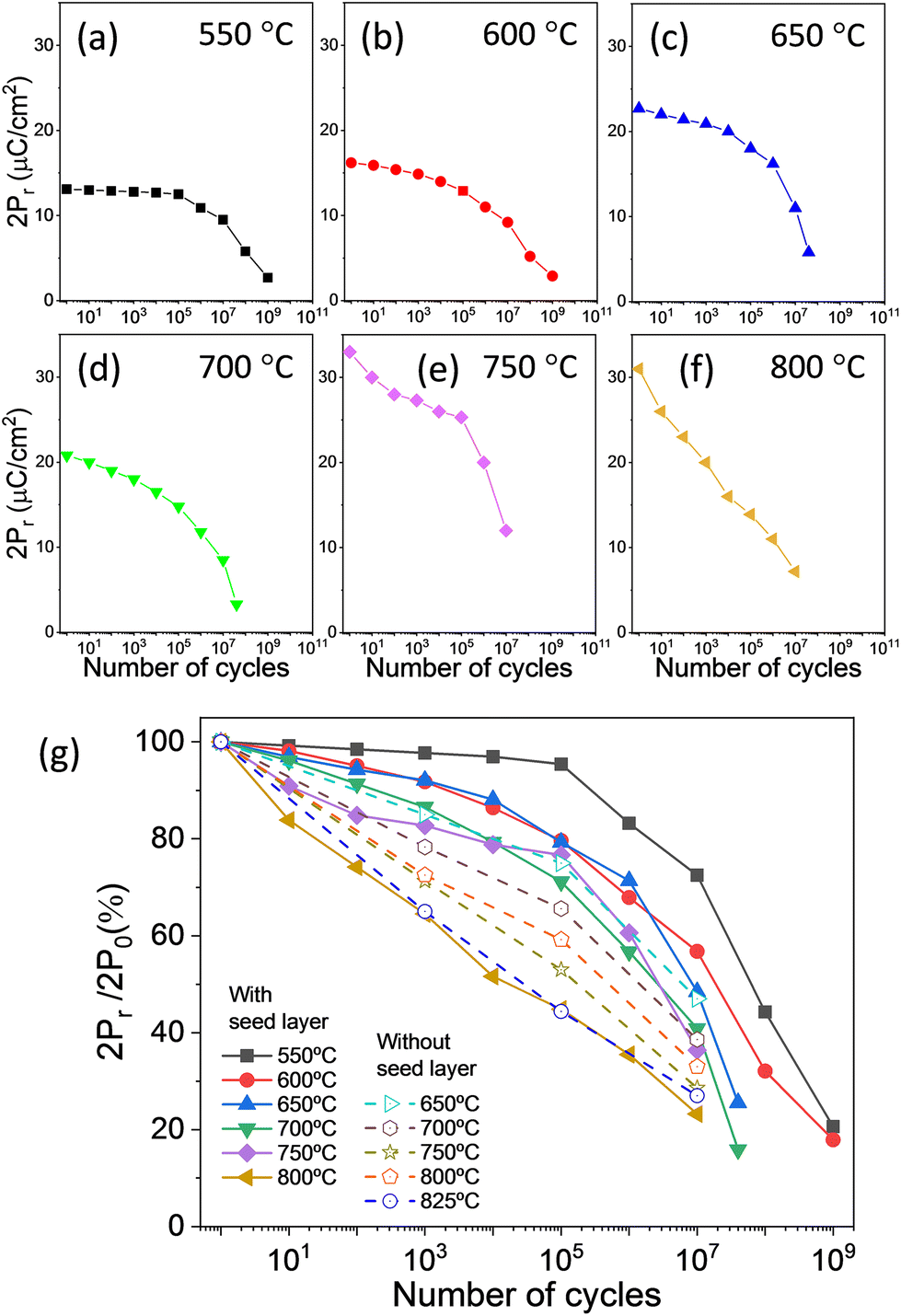 | ||
| Fig. 4 Endurance, measured with bipolar rectangular pulses of frequency 100 kHz and amplitude 4.5 V, of TS = 550 °C (a), 600 °C (b), 650 °C (c), 700 °C (d), 750 °C (e), and 800 °C (f) films on STO. (g) Comparison of endurance (remanent polarization is normalized to the pristine state value) of the films grown at various TS on a seed layer (solid symbols and solid lines) and films grown at various TS without a seed layer (empty symbols and dashed lines). Data of films grown without a seed layer are reported in ref. 35. | ||
It has been shown here that using an HZO seed layer, in comparison with films without it, allows enhancement of the crystalline quality, polarization and resistance against fatigue of ferroelectric HZO films. Also, it has been shown that lowering the growth temperature results in less polarization but also less fatigue. The decrease in polarization is a consequence of the reduced crystallization and the lower amount of orthorhombic phase in films deposited at low TS. Furthermore, there is a greater expansion of the out-of-plane lattice parameter with decreasing TS, indicating a higher density of point defects. On the other hand, epitaxial HZO on both substrates have high endurance despite the difference in the lattice parameter, therefore also discarding a strong effect on fatigue.35 Domain pinning at point defects is a possible mechanism of fatigue, but the lower fatigue in low TS films suggests that this is not a primary fatigue mechanism in epitaxial films. On the other hand, low TS films are less crystalline and may have extended defects. The higher number of point and extended defects in low-temperature deposited films probably cause the monotonic increase of leakage current in the pristine state with decreasing deposition temperature (Fig. 5, inset). Leakage (see ESI S10† for leakage curves) increases with cycling in all samples, particularly after 105–106 cycles, but the increase in low TS films is less and, after 107 cycles, the TS = 550 and 600 °C films have the lowest leakage. This may contribute to the high robustness of low TS films against electrical breakdown. Therefore, point and extended defects in films grown at low temperatures (Fig. 6) do not negatively affect endurance and, in contrast, may be a major factor for lower fatigue. We recently showed that the parasitic monoclinic phase has a positive effect on endurance, with less fatigue in films on STO substrates with coexisting orthorhombic and monoclinic phases than in almost pure orthorhombic films on scandate substrates.36 We argued that this is a consequence of the suppression of propagation of pinned domains at the boundaries with the non-ferroelectric phase. Here, in films grown at a lower temperature, a greater amount of monoclinic phase, point and extended defects and more defective grain boundaries between the orthorhombic and monoclinic phases could help suppress the rapid propagation of pinned domains.
 | ||
| Fig. 5 Evolution of the current leakage density with the number of cycles of the films on STO(001) deposited at the temperature indicated at the bottom right. Inset: pristine state leakage current density of films on STO(001) as a function of the deposition temperature. | ||
 | ||
| Fig. 6 Schematics of the expected amount of point (red color) and extended (blue color) defects as a function of the deposition temperature. | ||
4. Conclusions
In conclusion, the use of a seed layer allows the epitaxial growth of enhanced ferroelectric HZO films on STO(001) and Si(001) at a significantly lower temperature. The orthorhombic phase forms over a wide temperature range, with the (111) out-of-plane lattice parameter decreasing linearly with the deposition temperature by about 1.3%. The crystallization of the orthorhombic phase is reduced with decreasing substrate temperature and the polarization is slightly reduced. However, the films grown at low temperatures are more robust against ferroelectric fatigue and electrical breakdown. The results suggest that the pinning of ferroelectric domains at point defects is not a major mechanism of fatigue. The suppression of pinned domain propagation at more defective regions and grain boundaries in low-temperature deposited films is proposed as the reason for the enhancement.Conflicts of interest
There are no conflicts to declare.Acknowledgements
Financial support from the Spanish Ministry of Science and Innovation (MCIN/AEI/10.13039/501100011033), through the Severo Ochoa FUNFUTURE (CEX2019-000917-S), PID2020-112548RB-I00 and PID2019-107727RB-I00 projects, from Generalitat de Catalunya (2021 SGR 00804) and from CSIC through the i-LINK (LINKA20338) program is acknowledged. We also acknowledge project TED2021-130453B-C21, funded by MCIN/AEI/10.13039/501100011033 and European Union NextGeneration EU/PRTR. T. S. is financially supported by the China Scholarship Council (CSC) with No. 201807000104. T. S.'s work has been done as a part of his Ph.D. program in Materials Science at Universitat Autònoma de Barcelona. R. B. and G. S. G. acknowledge the financial support from the French National Research Agency (ANR) through the projects DIAMWAFEL (No. ANR-15-CE08-0034), LILIT (No. ANR-16-CE24-0022), and MITO (No. ANR-17-CE05-0018), as well as P. Regreny, C. Botella, and J. B. Goure for the technical support.References
- K. Sun, J. Chen and X. Yan, Adv. Funct. Mater., 2021, 31, 2006773 CrossRef CAS.
- M. H. Park, Y. H. Lee, T. Mikolajick, U. Schroeder and C. S. Hwang, MRS Commun., 2018, 8, 795–808 CrossRef CAS.
- X. Yan, Z. Xiao and C. Lu, Appl. Phys. Lett., 2020, 116, 013506 CrossRef CAS.
- M. H. Park, H. J. Kim, Y. J. Kim, W. Lee, T. Moon and C. S. Hwang, Appl. Phys. Lett., 2013, 102, 242905 CrossRef.
- H. A. Hsain, Y. Lee, G. Parsons and J. L. Jones, Appl. Phys. Lett., 2020, 116, 192901 CrossRef CAS.
- J. Wang, D. Zhou, W. Dong, Y. Yao, N. Sun, F. Ali, X. Hou and F. Liu, Adv. Electron. Mater., 2021, 7, 2000585 CrossRef CAS.
- M. H. Park, Y. H. Lee, T. Mikolajick, U. Schroeder and C. S. Hwang, Adv. Electron. Mater., 2019, 5, 1800522 CrossRef.
- Y. Tashiro, T. Shimizu, T. Mimura and H. Funakubo, ACS Appl. Electron. Mater., 2021, 3, 3123–3130 CrossRef CAS.
- T. Shimizu, K. Katayama, T. Kiguchi, A. Akama, T. J. Konno, O. Sakata and H. Funakubo, Sci. Rep., 2016, 6, 32931 CrossRef CAS.
- J. Lyu, I. Fina, R. Solanas, J. Fontcuberta and F. Sánchez, Appl. Phys. Lett., 2018, 113, 082902 CrossRef.
- P. Nukala, Y. Wei, V. de Haas, Q. Guo, J. Antoja-Lleonart and B. Noheda, Ferroelectrics, 2020, 569, 148–163 CrossRef CAS.
- I. Fina and F. Sánchez, ACS Appl. Electron. Mater., 2021, 3, 1530–1549 CrossRef CAS.
- Y. Wang, Q. Wang, J. Zhao, T. Niermann, Y. Liu, L. Dai, K. Zheng, Y. Sun, Y. Zhang, J. Schwarzkopf, T. Schroeder, Z. Jiang, W. Ren and G. Niu, Appl. Mater. Today, 2022, 29, 101587 CrossRef.
- J. Lyu, I. Fina, R. Solanas, J. Fontcuberta and F. Sánchez, ACS Appl. Electron. Mater., 2019, 1, 220–228 CrossRef CAS.
- J. Lyu, I. Fina, R. Bachelet, G. Saint-Girons, S. Estandía, J. Gázquez, J. Fontcuberta and F. Sánchez, Appl. Phys. Lett., 2019, 114, 222901 CrossRef.
- G. Saint-Girons, R. Bachelet, R. Moalla, B. Meunier, L. Louahadj, B. Canut, A. Carretero-Genevrier, J. Gazquez, P. Regreny, C. Botella, J. Penuelas, M. G. Silly, F. Sirotti and G. Grenet, Chem. Mater., 2016, 28, 5347–5355 CrossRef CAS.
- I. Fina, L. Fàbrega, E. Langenberg, X. Martí, F. Sánchez, M. Varela and J. Fontcuberta, J. Appl. Phys., 2011, 109, 074105 CrossRef.
- R. Meyer, R. Waser, K. Prume, T. Schmitz and S. Tiedke, Appl. Phys. Lett., 2005, 86, 142907 CrossRef.
- H. Y. Yoong, H. Wu, J. Zhao, H. Wang, R. Guo, J. Xiao, B. Zhang, P. Yang, S. J. Pennycook, N. Deng, X. Yan and J. Chen, Adv. Funct. Mater., 2018, 28, 1–10 CrossRef.
- M. A. Moram and M. E. Vickers, Rep. Prog. Phys., 2009, 72, 036502 CrossRef.
- P. F. Fewster, Rep. Prog. Phys., 1996, 59, 1339–1407 CrossRef CAS.
- S. Estandía, N. Dix, M. F. Chisholm, I. Fina and F. Sánchez, Cryst. Growth Des., 2020, 20, 3801–3806 CrossRef.
- S. Estandía, N. Dix, J. Gazquez, I. Fina, J. Lyu, M. F. Chisholm, J. Fontcuberta and F. Sánchez, ACS Appl. Electron. Mater., 2019, 1, 1449–1457 CrossRef.
- T. Song, R. Solanas, M. Qian, I. Fina and F. Sánchez, J. Mater. Chem. C, 2022, 10, 1084–1089 RSC.
- R. Takahashi, T. Yamamoto and M. Lippmaa, Cryst. Growth Des., 2021, 21, 5017–5026 CrossRef CAS.
- M. Mirjolet, F. Sánchez and J. Fontcuberta, Adv. Funct. Mater., 2019, 29, 1808432 CrossRef.
- S. Amoruso, A. Sambri and X. Wang, J. Appl. Phys., 2006, 100, 013302 CrossRef.
- A. Ojeda-G-P, M. Döbeli and T. Lippert, Adv. Mater. Interfaces, 2018, 5, 1701062 CrossRef.
- H. N. Lee, S. S. A. Seo, W. S. Choi and C. M. Rouleau, Sci. Rep., 2016, 6, 19941 CrossRef CAS.
- J. V. Barth, G. Costantini and K. Kern, Nature, 2005, 437, 671–679 CrossRef CAS.
- J. Lyu, I. Fina, R. Solanas, J. Fontcuberta and F. Sánchez, Sci. Rep., 2018, 8, 495 CrossRef.
- P. Jiang, Q. Luo, X. Xu, T. Gong, P. Yuan, Y. Wang, Z. Gao, W. Wei, L. Tai and H. Lv, Adv. Electron. Mater., 2021, 7, 2000728 CrossRef CAS.
- J. P. B. Silva, K. C. Sekhar, R. F. Negrea, J. L. MacManus-Driscoll and L. Pintilie, Appl. Mater. Today, 2022, 26, 101394 CrossRef.
- F. Cüppers, K. Hirai and H. Funakubo, Nano Convergence, 2022, 9, 56 CrossRef.
- J. Lyu, I. Fina and F. Sánchez, Appl. Phys. Lett., 2020, 117, 072901 CrossRef CAS.
- T. Song, S. Estandía, H. Tan, N. Dix, J. Gàzquez, I. Fina and F. Sánchez, Adv. Electron. Mater., 2021, 8, 2100420 CrossRef.
Footnote |
| † Electronic supplementary information (ESI) available: XRD pole figures. XRD 2θ–χ maps measured with a 2D detector. Simulation of Laue fringes. XRD θ–2θ scans of the HZO films deposited on Si(001). Current–voltage loops measured in the HZO films deposited on STO(001). Current–voltage and the corresponding polarization–voltage loops of the HZO films deposited on Si(001). PUND measurements. Polarization–voltage loops measured in the pristine state and after the indicated number of cycles. Polarization retention measurements for films on STO(001). Leakage current curves measured in the pristine state and after the indicated number of cycles. See DOI: https://doi.org/10.1039/d2nr05935e |
| This journal is © The Royal Society of Chemistry 2023 |