
 Open Access Article
 This Open Access Article is licensed under a
 Creative Commons Attribution 3.0 Unported Licence
Chalcogen (S, Se, and Te) decorated few-layered Ti3C2Tx MXene hybrids: modulation of properties through covalent bonding†
Jalal
Azadmanjiri
*,
Pradip Kumar
Roy
,
Lukáš
Děkanovský
and
Zdeněk
Sofer
 *
*
Department of Inorganic Chemistry, University of Chemistry and Technology Prague, Technická 5, 166 28 Prague 6, Czech Republic. E-mail: jalal_azad2000@yahoo.com; jalal.azadmanjiri@vscht.cz; zdenek.sofer@vscht.cz
First published on 5th January 2023
Abstract
2D carbides and nitrides of transition metals (MXenes) have shown great promise in a variety of energy storage and energy conversion applications. The extraordinary properties of MXenes are because of their excellent conductivity, large carrier concentration, vast specific surface area, superior hydrophilicity, high volumetric capacitance, and rich surface chemistry. However, it is still desired to synthesize MXenes with specific functional groups that deliver the required characteristics. This is due to the fact that a considerable amount of metal atoms is exposed on the surface of MXenes during their synthesis through an etching procedure; hence, other anions and cations are uncontrollably implanted on their surfaces. Because of this situation, the first invented Ti3C2Tx MXene suffers from low photoresponsivity and detectivity, large overpotential, and small sensitivity in photoelectrochemical (PEC) photodetectors, hydrogen evolution reaction (HER), and sensing applications. Therefore, surface modification of the MXene structure is required to develop the device's performance. On the other hand, there is still a lack of understanding of the MXene mechanism in such cutting-edge applications. Thus, the manipulations of MXenes are highly dependent on understanding the device mechanism, suitable modification elements, and modification methods. This study for the first time reveals the conjugation effect of pre-selected S, Se, and Te chalcogen elements on a few-layered Ti3C2Tx MXene to synthesize new composites for PEC photodetector, HER, and vapor sensor applications. Also, the mechanism of the chalcogen decorated few-layered Ti3C2Tx MXene composites for each application is discussed. The selection of a few-layered Ti3C2Tx MXene is due to its fascinating characteristics which make it capable to be considered as an appropriate substrate and incorporating chalcogen atoms. The Te-decorated few-layered Ti3C2Tx MXene composite provides better performances in PEC photodetector and vapor sensing applications. Although the potential value of the Se-decorated few-layered Ti3C2Tx composite is slightly lower than that of the Te-decorated sample in HER application, its overpotential is still greater than that of the Te-decorated sample. The acquired results show that the S-decorated few-layered Ti3C2Tx composite demonstrates the lowest performance in all three examined applications in comparison with the other two samples.
1. Introduction
High-efficiency photodetectors, electrocatalysts, sensors, and many more other state-of-the-art devices, require robust nanostructures that overcome the current limitations of those instruments. Two-dimensional (2D) nanomaterials are capable of providing unique properties because of their attractive physical (i.e., electrical- and photo-conductivity), chemical (i.e., catalytic activity), and mechanical (i.e., high stability) properties.1–6 These fascinating characteristics of 2D nanomaterials are due to their ultrathin planar structures which result in strong quantum confinement and their large surface area.7–9 Among the different varieties of invented and synthesized 2D nanomaterials, transition-metal carbides and carbonitrides (MXenes) have demonstrated admirable performances because of their wide specific surface area, and tendency to be bonded covalently with guest atoms because of the inner metal vacancies which are generated during their synthesis.10–12 In addition to these, the high electrical conductivity, tunable bandgap, and great mechanical stability of MXenes make them suitable candidates for energy storage and conversion without decomposition of the structure.13–16Four molecular structures of M2X, M3X2, M4X3, and M5C4 MXene nanosheets (M and X stand for transition metal elements, and C or N elements, respectively) have been made accessible so far with single-, few- and multi-layer structures,17 and the sizes of a few micrometers to the recently achieved ultra-large flakes.18 Surface termination species (Tx) or intercalated compounds (ICs) are replaced with the “A” atoms as a result of the A-layer selective etching from the initial MAX phase. The resulting MXenes have a chemical formula of Mn+1XnTx or Mn+1XnTx-IC after the substitution of the end groups by the intercalation.19 Tx and ICs could be ![[double bond, length as m-dash]](https://www.rsc.org/images/entities/char_e001.gif) O, –H, –OH, or –F, and NH4+ or NH3 groups depending on the etchant employed and the etching process parameters (i.e., etching time, etching temperature, etc.).20–22 In addition, the hydrophilicity of MXene nanosheets is discovered to be caused by these functional groups of Tx and ICs.21 Furthermore, the nature of MXenes is capable of being changed by its functional groups. For instance, the full functionalization of Ti3C2Tx MXenes with O can turn the metallic nature of the MXenes into a semiconductor state with a significant Seebeck coefficient.23
O, –H, –OH, or –F, and NH4+ or NH3 groups depending on the etchant employed and the etching process parameters (i.e., etching time, etching temperature, etc.).20–22 In addition, the hydrophilicity of MXene nanosheets is discovered to be caused by these functional groups of Tx and ICs.21 Furthermore, the nature of MXenes is capable of being changed by its functional groups. For instance, the full functionalization of Ti3C2Tx MXenes with O can turn the metallic nature of the MXenes into a semiconductor state with a significant Seebeck coefficient.23
It has been investigated as a benchmark that the Ti3C2Tx MXene has shown promising performance in energy storage and conversion. However, despite its high electronic conductivity and excellent performance in comparable electrolytic systems, it does not function well in some applications such as self-powered photoelectrochemical (PEC) photodetectors, hydrogen evolution reaction (HER) electrocatalysis, and vapor sensing applications. For instance, terminated Ti3C2Tx MXenes have shown a large overpotential for the HER in aqueous electrolytes despite being predicted to be active in that application.24,25 In this regard, significant efforts are required to first understand the underlying mechanisms behind the low performance of Ti3C2Tx MXenes, and then, attempt to develop the efficiency of the MXenes with appropriate approaches like promoting charge transfer, H+/e− couplings, and surface catalytically active sites in such applications.
Herein, we report a solid-state annealing strategy to investigate the decorating effect of the pre-selected chalcogen (S, Se, and Te) atoms on the performance of few-layered Ti3C2Tx MXenes in the aforementioned applications, as well as explain their mechanisms. This will reveal information about the active sites and how the distribution of electrons varies under reactional conditions. The PEC photodetector, HER, and vapor sensing working mechanisms of blank and chalcogen decorated few-layered Ti3C2Tx MXenes with S, Se, and Te elements are yet unclear and to the best of our knowledge, there are no published studies to explain those systems. This lack of studies can partially be attributed to the undesirable Ti3C2Tx MXene with low charge transfer and large overpotential. Thus, this work provides insight into modifications and conditions to enable improvement of the deficiencies through structural analyses. The chalcogen elements as a decoration agent have been chosen due to their high electronegativity, rich d-electron, large dipole atomic polarizability, high photoconductivity, and high responsivity characteristics.26–28
2. Experimental methods
2.1. Sample preparation
 | ||
| Scheme 1 A schematic illustration of the (a–e) step-by-step procedure for synthesizing few-layered Ti3C2Tx and chalcogen decorated Ti3C2Tx MXenes via HF etching, TBAOH, and solid-state annealing technique, respectively, and (f) applications of few-layered chalcogen decorated Ti3C2Tx MXenes for PEC photodetector, HER, and gas sensors. | ||
![[thin space (1/6-em)]](https://www.rsc.org/images/entities/char_2009.gif) :1 chalcogen were firstly weighed and inserted in a quartz glass ampule (Scheme 1d and e) and evacuated to 1 × 10⁻⁵ mbar with a diffusion pump and melt sealed. Following sealing with an oxygen–hydrogen torch, the quartz ampule was subsequently placed inside a muffle furnace and heated at 500 °C for 24 h using a 5 °C min−1 heating and cooling rate. Finally, the chalcogen decorated few-layered Ti3C2Tx composite powders were manually collected from the broken quartz tube.
:1 chalcogen were firstly weighed and inserted in a quartz glass ampule (Scheme 1d and e) and evacuated to 1 × 10⁻⁵ mbar with a diffusion pump and melt sealed. Following sealing with an oxygen–hydrogen torch, the quartz ampule was subsequently placed inside a muffle furnace and heated at 500 °C for 24 h using a 5 °C min−1 heating and cooling rate. Finally, the chalcogen decorated few-layered Ti3C2Tx composite powders were manually collected from the broken quartz tube.
2.2. Characterization methods
3. Results and discussion
3.1. Crystal, morphological and chemical characterization
The crystal phases, structure, and morphology of the synthesized Ti3C2Tx and chalcogen (S, Se, and Te) decorated few-layered Ti3C2Tx MXenes (namely; Te/Ti3C2Tx, Se/Ti3C2Tx, and S/Ti3C2Tx) were characterized by XRD, SEM, and TEM/HRTEM. As depicted in the XRD characterization of Fig. 1, Aluminium (Al) layers of the Ti3AlC2 MAX phase were almost terminated after etching with 40% HF to gain the Ti3C2Tx MXene. The obtained Ti3C2Tx MXene also show a well-crystallized form. The critical heating temperature for the Ti3C2Tx MXene chemical and structural phase transitions has been estimated to be around 850 °C.30 Thus, a benign annealing temperature of 500 °C was implemented to just modify the surface chemistry and thermally break down the functional groups. Subsequently, it has been observed from the XRD patterns of Te/Ti3C2Tx, Se/Ti3C2Tx, and S/Ti3C2Tx samples that the (002) and (004) peaks completely disappeared and were substituted by a group of sharp diffraction peaks that index mainly to Te and formed-Ti0.95Te0.05 (in Te/Ti3C2Tx), formed-TiSe2 (in Se/Ti3C2Tx), formed-TiS2 and TiS (in S/Ti3C2Tx), TiO2 (in all samples), and some other compounds belonging to the Ti3C2 MXene and decorated chalcogen. It is hypothesized that a direct reaction between chalcogen elements and MXene layers which took place at 500 °C under vacuum conditions caused the majority formation of those chemical bonding and phases. The chemical reaction and bonding generally could be based on the fact that an atom from the surface functional groups (O, –H, –OH, or –F) of the Ti3C2Tx structure leaves its initial position (mostly –OH and some parts of –F)30 at temperatures below the annealing's critical point, and then a vacancy is created that can be filled with chalcogen atoms and create covalent bonding with the nearby atoms. As a result, the elimination of –OH and maybe some portion of –F causes the formation of Ti0.95Te0.05, TiSe2, TiS2, and TiS on the surface of the MXene. A small degree of chemical reaction could be noticed between the Te chalcogen and Ti3C2Tx MXene in the Te/Ti3C2Tx sample. This low reaction of Te with MXene might be attributed to the high boiling point of Te (∼988 °C) in comparison with the other S (∼445 °C) and Se (∼685 °C) chalcogen elements, where the annealing temperature applied at 500 °C is very less for a large chemical reaction for Te. The other formation phases of SeO2 (in Se/Ti3C2Tx) and C2S (in S/Ti3C2Tx) are also because of the existence of O terminations on the MXene and the vacancy of Ti, respectively. The existence of the TiO2 phase is also not astonishing because the annealed chalcogen decorated few-layered Ti3C2Tx MXenes contained oxygen-containing species and a portion of –F surface terminations that are known to stabilize the TiO2 anatase phase.31,32 Regularly, the etching treatment procedure is frequently recognized to crumble the hexagonal crystal structure and P63/mmc symmetry of the MAX phase by elimination of A-layers. Nonetheless, the surface terminations on the MXene by intercalation of termination ions hold a portion of the hexagonal symmetry components of the parent MAX material. The SEM, TEM, electron diffraction pattern and HRTEM images of the synthesized S/Ti3C2Tx, Se/Ti3C2Tx, and Te/Ti3C2Tx can confirm the structural stability of the Ti3C2Tx MXene after annealing under vacuum conditions in the presence of the chalcogen decoration agents and also the formation of the aforementioned formed phases (Fig. 1b–d). These results of characterization are consistent with the XRD results that demonstrate the various morphologies formed in the chalcogen decorated few-layered Ti3C2Tx MXene composite, without decomposition of the Ti3C2Tx MXene support after annealing.
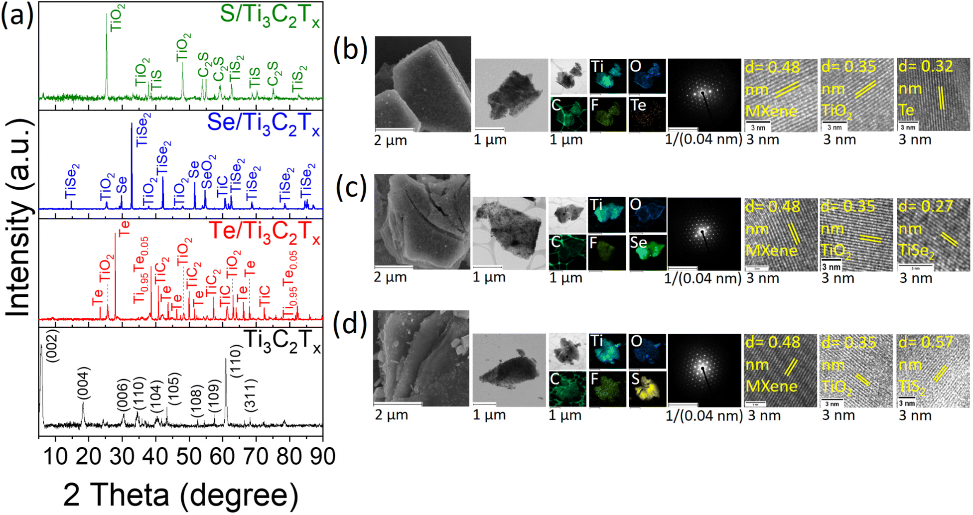 | ||
| Fig. 1 Structural and morphological characterization of Ti3C2Tx, Te/Ti3C2Tx, Se/Ti3C2Tx, and S/Ti3C2Tx; (a) XRD, (b–d) typical SEM, TEM including elemental mappings, electron diffraction, and HRTEM of Te/Ti3C2Tx, Se/Ti3C2Tx, and S/Ti3C2Tx. (Note: the TEM and elemental mapping images of the synthesized Ti3C2Tx have been provided in Fig. S1.†) | ||
To further analyze the surface chemistry, chemical states, and atomic bonding configurations, the as-received Ti3AlC2 MAX and synthesized Ti3C2Tx, Te/Ti3C2Tx, Se/Ti3C2Tx, and S/Ti3C2Tx MXenes were subjected to XPS characterization (Fig. S2† and Fig. 2a–c). The full XPS survey and high-resolution spectra could represent the distinct signals of Ti, C, O, F, S, Se, and Te elements. The samples’ XPS analysis reveals that after annealing them with pre-selected chalcogen elements, the amount of F species significantly decreased while the content of O increased slightly. Similar results have been observed in single Se atoms on Ti3C2Tx MXene nanosheets under CO2 conditions,26 as well as in our other recent work by the solid-state annealing method.33 This variation would be due to the substitution in termination contents by chalcogen elements and oxygen-containing terminations (like Ti–O, C–O, S–O, and Se–O). High-resolution XPS spectra of the elements of the samples can further help evaluate the changes in chemical states and their occupancy after decoration of the few-layered Ti3C2Tx MXene with Te, Se, and S (Fig. 2a–c). The Ti 2p peaks of the samples are devoted to certain bonds belonging to Ti–O (bond in TiO2) and Ti–C (bond in Ti3C2Tx).34,35 The C 1s and O 1s peaks are assigned to C–Ti, C–C, Se–C, S–C, C–O, and Ti–O bonds. In the XPS spectra of the Se 3d, S 2p, and Te 3d, peaks are ascribed to the anchoring of chalcogen elements on Ti3C2Tx.
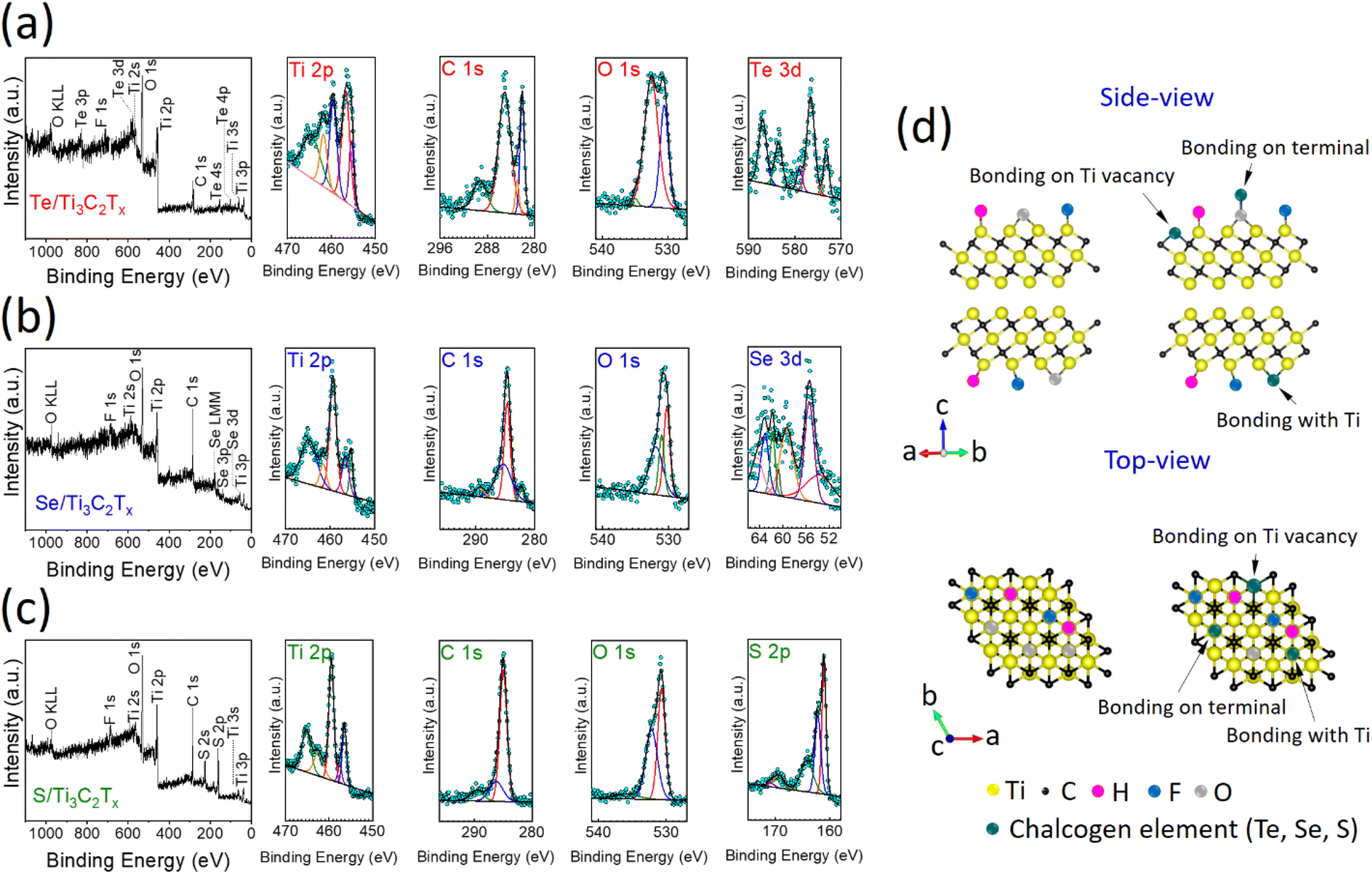 | ||
| Fig. 2 XPS survey spectrum and high-resolution elemental spectra of (a) Te/Ti3C2Tx, (b) Se/Ti3C2Tx, and (c) S/Ti3C2Tx. (d) Schematic illustration of possible potential anchoring sites for the chalcogen decorated few-layered Ti3C2Tx MXene composite (side- and top-view). | ||
There are three likely potential anchoring sites that could incorporate the chalcogen agent atoms to be bonded with the Ti3C2Tx MXene (Fig. 2d). These three possibilities are: (i) bonding with the terminal groups on the surface and producing chalcogen–oxygen species, (ii) bonding with Ti atoms like surface terminals on Ti3C2Tx, and (iii) occupying the Ti vacancies that already have been created during the etching process of Ti3AlC2 MAX. The XRD and XPS analyses indicate that at a 500 °C annealing temperature under 10−5 mbar vacuum conditions, chalcogen atoms are prone to bond with any of those three alternatives. Formation of the TiSe2, TiS, and TiS2 phases in considerable quantities, however, supports the chemical bonding arrangement of Se and S with Ti. The nature of this chemical bonding is perhaps due to the leaving of the functional group components of –OH and –F at this annealing temperature and providing low formation energy for the formation of Ti–Se, Ti–S, and Ti–Te bonds. This situation could be observed as insignificant in the case of the Te chalcogen with the Ti3C2Tx MXene maybe because of its high boiling temperature, and low thermal-annealing energy for the formation of chemical reaction bonding.
3.2. PEC photodetector
To discover the photoresponse performance of the chalcogen decorated few-layered Ti3C2Tx MXene, the photocurrent density of the samples was examined and compared to those of the blank ITO substrate, as-received Ti3AlC2 MAX phase, and synthesized few-layered Ti3C2Tx MXene. In this instance, a three-electrode setup was used to perform PEC characterization along with an appropriate sample dropped onto the conductive ITO wafer. Several LED light illumination of 420 nm, 460 nm, 385 nm, and 532 nm with a power of 800 mW were used to measure the dependence of the photocurrent on the wavelength. Fig. 3a depicts the representative potential–current density (V–I) curve for the synthesized few-layered Ti3C2Tx MXene that was obtained using linear sweep voltammetry in 1 M KOH at a scan rate of 10 mV s−1. It shows a distinct response to the 420 nm LED illumination when it is turned on and off along with a steady increase in current density against the evolution of the applied voltage. | ||
| Fig. 3 (a) A representative anodic scan of a few-layered Ti3C2Tx sample in 1 M KOH under 420 nm LED illumination. Photocurrent density of (b) Te/Ti3C2Tx, (c) Se/Ti3C2Tx, and (d) S/Ti3C2Tx samples under the illumination of 420 nm, 460 nm, 385 nm, and 532 nm LED sources in 1 M KOH solution at 1.25 V vs. SCE. | ||
The photocurrent density characterization of the ITO substrate, Ti3AlC2, and Ti3C2Tx samples revealed very low to negligible current density ranges with 420 nm, 460 nm, and 532 nm illumination (Fig. S3†). Among the Ti3AlC2 and Ti3C2Tx samples, the Ti3C2Tx MXene illustrates a higher current density (1.2 μA cm−2) than the Ti3AlC2 with only 0.3 μA cm−2 under the 420 nm illumination. Nevertheless, this current density value is still away from an arbitrary state. Besides, the current density of the Ti3C2Tx MXene is also low under the other 460 nm (0.5 μA cm−2) and 532 nm (0.4 μA cm−2) illumination. Following that, the photocurrent activity of the chalcogen decorated Ti3C2Tx composites was also evaluated. The collected results not only show an extraordinary photocurrent density of 12 μA cm−2 (Te/Ti3C2Tx with 420 nm illumination), but also some other current density values were collected under 460 nm, 385 nm, and 532 nm illumination (Fig. 3b–d) which are almost equal to the maximum value of the Ti3C2Tx sample under 420 nm. A steady stable state was observed in the current density of the chalcogen decorated few-layered Ti3C2Tx composite samples with passing time. However, it can be seen that the current density value shows fluctuation in the blank few-layered Ti3C2Tx sample with 460 nm and 532 nm LED lights. This achievement is probably due to the unstable condition of the sample on top of the ITO substrate. The value of response time, another important parameter in photodetectors, was determined on the representative Te/Ti3C2Tx sample. The obtained results show a swift response and recovery time of ∼1.0 s toward the illumination light (Fig. 4).
 | ||
| Fig. 4 A representative single-cycle response time, semi-cycle response, and recovery times of the PEC Te/Ti3C2Tx photodetector in 1 M KOH solution under the 420 nm LED light with a power of 800 mW. | ||
In order to gain further insight into the efficiency of the PEC photodetector, the responsivity (R) values of the Ti3C2Tx, Te/Ti3C2Tx, Se/Ti3C2Tx, and S/Ti3C2Tx samples were assessed using  , where ΔI is the difference in the photocurrent density with respect to the dark current, and P is the irradiance power intensity per unit area (Fig. S4a† and Fig. 4a–c).33
It can be observed that the responsivity of the Te/Ti3C2Tx sample (Fig. 5a) reaches 70 μA W−1 which is almost 20 times higher than the responsivity of blank few-layered Ti3C2Tx (Fig. S4a†) and even possesses a higher value in comparison with the other Se/Ti3C2Tx (Fig. 5b) and S/Ti3C2Tx (Fig. 5c) samples. For further additional characterization, it is essential to evaluate the specific detectivity of a photodetector device which describes the minimum illumination power necessary for a photodetector to distinguish the signal from noise. Thus, the following formula is utilized to calculate the specific detectivity:  , where A and B represent the active area and measured bandwidth, respectively, and NEP represents noise-equivalent power.36,37 NEP is defined as the input signal power that produces a signal-to-noise ratio (S/R) of one in an output bandwidth of 1 Hz. It also can be expressed as follows:
  , where IN is the noise current (dark current) and Rph is the photodetector's photoresponsivity.37Fig. 4d–f display the detectivity of Te/Ti3C2Tx, Se/Ti3C2Tx, and S/Ti3C2Tx samples, respectively. The maximum detectivity between the chalcogen decorated Ti3C2Tx composite samples is likely due to the high carrier concentration at low dark current densities for the Te/Ti3C2Tx sample with ∼4.5 × 108 cm Hz1/2 W−1 (Fig. 5d). The detectivity value for Se/Ti3C2Tx and S/Ti3C2Tx samples is ∼3.0 × 108 cm Hz1/2 W−1 and ∼1.5 × 107 cm Hz1/2 W−1, respectively. On the other hand, the detectivity of the few-layered blank Ti3C2Tx is ∼1.2 × 107 cm Hz1/2 W−1 (Fig. S4b†).
 | ||
| Fig. 5 The responsivity (a–c) and detectivity (d–f) of PEC Te/Ti3C2Tx, Se/Ti3C2Tx, and S/Ti3C2Tx photodetectors, respectively, in 1 M KOH solution as a function of power density upon 420 nm, 460 nm, and 532 nm illumination wavelengths. | ||
The low photodetection characteristic of the Ti3C2Tx MXene could be attributed to the crystal defects which usually are formed on the Ti3C2Tx MXene during the etching process of the Ti3AlC2 MAX phase. Those defects would represent a trap and then capture the photogenerated electron–hole pairs. On the other hand, the optical bandgap of the blank few-layered Ti3C2Tx MXene has the highest value among the presented materials (Fig. 6a) of ∼3.7 eV. This high value of the optical bandgap is due to the concentration of defects on the Ti3C2Tx MXene, where the excess defect density shifts the Fermi level towards the conduction band, thereby giving rise to the Moss–Burstein effect and optical bandgap.38 Hence, this high optical bandgap value of the Ti3C2Tx MXene could be another possible reason for the lower performance in its photodetector activities. In the case of the chalcogen decorated few-layered Ti3C2Tx MXene composite samples, those formation vacancies usually are occupied by the chalcogen elements. Therefore, photocurrent density could be developed in such decorated composite samples. Also, the optical bandgap of chalcogen decorated samples (Fig. 6a) declined to a lower value which has a beneficial effect on generation charge carriers and developing photocurrent density. The specific surface area of all samples also was analyzed using Brunauer–Emmett–Teller (BET) measurements. Fig. 6b shows that the surface area value of the Ti3C2Tx MXene is lower than those of the other samples. This results in a low active surface area and subsequently, low charge carriers and photocurrent density for that sample. Although the surface area of S/Ti3C2Tx is higher than those of the other two chalcogen decorated composite samples (Te/Ti3C2Tx and Se/Ti3C2Tx), the higher photocurrent density of Te/Ti3C2Tx is due to another physical phenomenon of ionization energy. One can speculate that an element with lower ionization energy can generate higher electron–hole pairs since the ionization energy is the minimum energy required to separate the most loosely bound electron. A comparison between the ionization energy of the chalcogen elements confirms that the ionization energy of Te is lower than those of the other two chalcogen elements (ionization energy: Te < Se < S).39 This causes the enhancement of photocurrent density, photoresponsivity, and detectivity of Te/Ti3C2Tx in comparison with the other Se/Ti3C2Tx and S/Ti3C2Tx samples. The formation of transition metal dichalcogenides on top of Se- and S-decorated Ti3C2Tx MXenes in this work is the other possible reason for developing photodetection activities of the Ti3C2Tx due to the high charge carrier mobility of those shaped phases.40
 | ||
| Fig. 6 (a) UV-Vis absorption spectra along with Tauc plots of the blank and chalcogen decorated Ti3C2Tx composite samples. (b) BET analysis of (i) blank Ti3C2Tx MXene, (ii) Te/Ti3C2Tx (210 pm), (iii) Se/Ti3C2Tx (190 pm), and (iv) S/Ti3C2Tx (180 pm) samples. | ||
3.3. Hydrogen evolution reaction
The electrocatalytic efficiency of the chalcogen decorated Ti3C2Tx MXene composite samples for the HER was evaluated by conducting linear sweep voltammetry (LSV) in an acidic environment (0.5 H2SO4). The achieved results were then compared with those of blank few-layered Ti3C2Tx MXene, platinum–carbon (PtC, 1%), and GC substrate under the same experimental conditions to assess the origin of the developed HER performance of the chalcogen decorated influence on the Ti3C2Tx MXene (Fig. 7). According to the typical overpotential value at a −10 mA cm−2 current density for the HER, the evaluated overpotentials for the chalcogen decorated few-layered Ti3C2Tx MXene composite samples illustrate an improvement in catalytic performance because of the new active sites as well as a newly formed phase by chalcogen decorated atoms. The Tafel analysis was also carried out to determine the electrochemical kinetics. Its slope identifies a logarithm of current density with overpotential and provides a simple way to recognize the rate-determining step, and hence, a possible electrochemical mechanism in the HER. It is observed from Fig. 7a that the Se/Ti3C2Tx sample is willing to generate bonding sites with hydrogen atoms easier than the other measured samples. Generally, the possible mechanisms for the HER in acidic media could be based on the Volmer–Heyrovsky or Volmer–Tafel mechanism. The Volmer process always occurs at the initial step, and it is followed by either the Heyrovsky or Tafel process. However, one of Heyrovsky's or Tafel's actions would be as a predominant mechanism. For the Volmer step to be the rate-determining step, it already has been proven that the magnitude of the Tafel slope has to be around 120 mV dec−1.41,42 This value for the corresponding mechanisms of the Heyrovsky and Tafel step is observed at around 40 and 30 mV dec−1, respectively.41,43 The Tafel slopes for each sample were obtained from the linear portion of the polarization curves (Fig. 7b). It can be seen that the slope values are as follows: PtC 1% ∼ 163 mV dec−1, Se/Ti3C2Tx ∼ 223 mV dec−1, Te/Ti3C2Tx ∼ 204 mV dec−1, S/Ti3C2Tx ∼ 220 mV dec−1, Ti3C2Tx ∼ 248 mV dec−1, and GC ∼ 227 mV dec−1. According to the above explanations for the HER mechanism in acidic media and the acquired distinct Tafel slope values of the samples, it can be proposed that another different mechanism would occur for both blank and chalcogen decorated Ti3C2Tx MXene composite samples that would be determined based on the following hypothesis. In the case of the blank Ti3C2Tx MXene, oxygen (O) terminal groups could be protonated with the existing high concentration of H+ in the H2SO4 electrolyte resulting in Ti–OH bonding. This protonation could be followed by the adjacent Ti site and lead to the formation of H2. Nonetheless, it is observed from Fig. 7b that the blank Ti3C2Tx MXene suffers from a 248 mV dec−1 large overpotential value. This high overpotential value is maybe attributed to the lack of an ideal equilibrium between Ti and O sites in this sample.44 In the case of the chalcogen decorated Ti3C2Tx MXene composite samples, it already was proven by XPS characterization (Fig. S2† and Fig. 2) that the O content was enhanced slightly after decoration. Therefore, this variation in the O content legitimized the evolution of more H2 contents in the modified samples. Likewise, the arrangement of Ti0.95Te0.05, TiSe2, TiS, and TiS2 phases in the chalcogen decorated Ti3C2Tx composite samples is roughly unattainable to be stoichiometric, perhaps due to chalcogen vacancies.45–47 The chalcogen vacancies and strain are also shown frequently to be the active sites in catalysts to maximize HER performance.48–50 Also, the loss of chalcogen causes additional electrons to be redistributed among the nearby atoms.51 As a result, the chalcogen vacancies at the surface of the chalcogen decorated Ti3C2Tx composite sample may drive electron accumulation, which creates more active sites and speeds up the reaction rate of the H+/e− coupling and the generation of additional H2 with a lowering overpotential value.
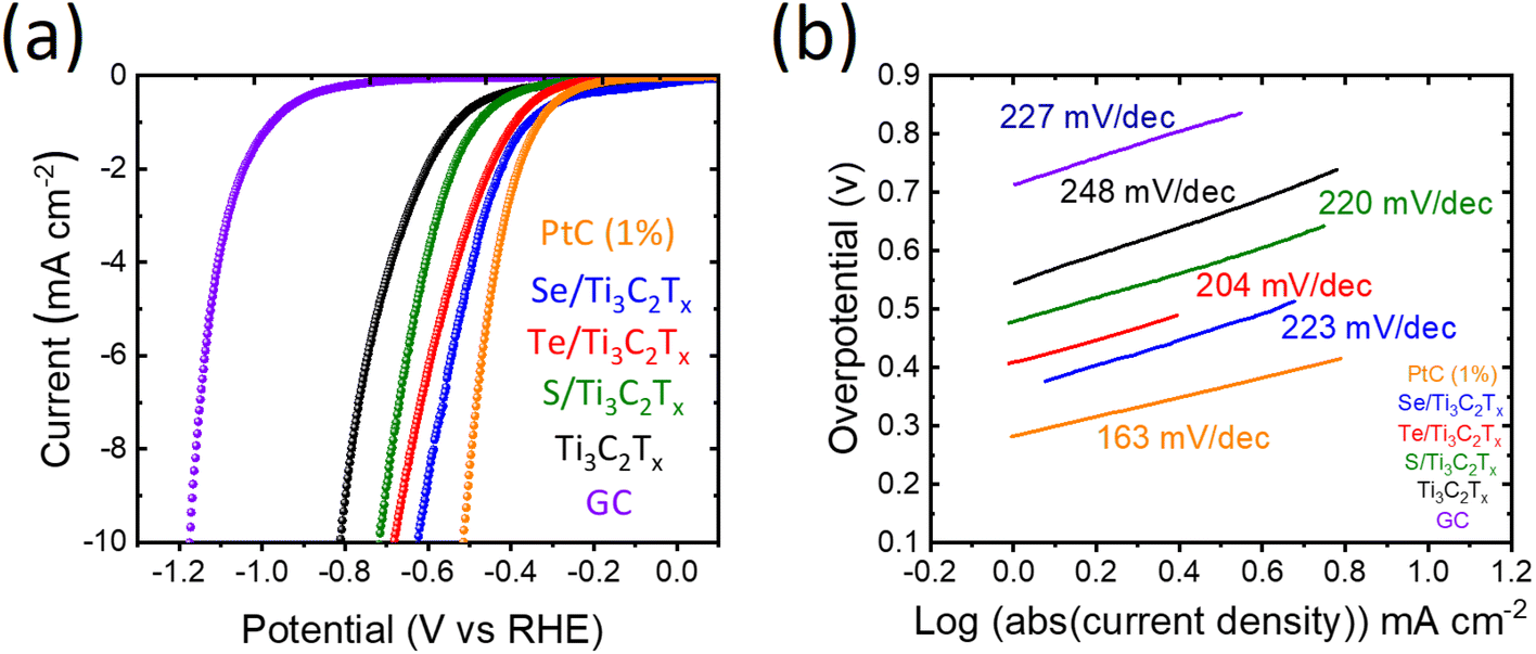 | ||
| Fig. 7 HER analysis of the blank Ti3C2Tx MXene, Te/Ti3C2Tx, Se/Ti3C2Tx, and S/Ti3C2Tx samples in 0.5 M H2SO4 medium and compared with GC and PtC (1%) samples. (a) Polarization curves and (b) Tafel plots of the corresponding overpotentials. | ||
3.4. Vapor sensors
The improvement of cutting-edge gas sensor devices for tracking down a low-level density of volatile organic molecules is necessary. In this context, MXenes have been evaluated for gas sensors in view of their remarkable attributes, recently,52–54 albeit the gas and vapor detection by MXenes has been viewed as more convoluted as opposed to the other 2D nanomaterials with surface adsorption and a regular charge movement.55,56 This is maybe attributed to the layered accordion-like structure of MXenes, where the interlayers are able to swell and affect the gas response. To investigate the gas sensing efficiency of the chalcogen decorated few-layered Ti3C2Tx MXene composites and compare it with the pristine Ti3C2Tx, herein, we used the electrochemical impedance spectroscopy strategy and evaluated the samples on some polar organic vapors of methanol, ethanol, and acetone. The detection of the gases by MXenes generally occurs based on the sensitivity level of the impedance signals derived from the variety of the local carrier on the MXene layers. The Nyquist and Bode (impedance phase spectra) plots of the specimens are shown in Fig. 8. It can be observed from the Nyquist plots that all of the sample's behavior with the examined gases is like that of a series RC circuit. Also, it can be recognized that the resistance, combined capacitance, and inductance belonging to the real and imaginary sections of impedance (Z′ and Z′′) have been enhanced in the chalcogen decorated few-layered Ti3C2Tx composite, especially for the Te/Ti3C2Tx and Se/Ti3C2Tx samples, in the presence of all vapors (Fig. 8). This Z′ and Z′′ increment could probably be due to the increased oxygen content, and subsequently, the formation of TiO2 with an electrical resistivity of 1012 Ω cm−1,57 as well as the other formed phases during decoration of Ti3C2Tx with chalcogen elements. A comparison between the Bode phase plots of the pristine and chalcogen decorated few-layered Ti3C2Tx composite samples indicates an enhanced affinity in the sensitivity of the Te/Ti3C2Tx and Se/Ti3C2Tx MXene samples. Amongst the latest two samples, Te/Ti3C2Tx sensing performance seems to be even better maybe due to the less chemical reaction of Te with Ti3C2Tx. However, this trend is almost unchanged for the other S/Ti3C2Tx in comparison with the pristine Ti3C2Tx. The sensing mechanism of chalcogen decorated Ti3C2Tx composite samples with a positive variation could be discussed based on the following points of view: (i) the –F terminals with a detrimental effect on gas sensing have been reduced in chalcogen decorated Ti3C2Tx samples.55 (ii) The high polarity of the applied organic gases (methanol, ethanol, and acetone) and the interaction of those polar molecules with the enhancedO terminals on the surface of the samples lead to charge transfer through the formation of hydrogen bonds. (iii) More electrons are produced on the surface of the chalcogen decorated Ti3C2Tx composite samples as a result of the rich d-electrons of chalcogen elements and non-stoichiometric produced phases. This could increase the interaction of polar molecules with the sample and then enhance the extent of charge transfer. The suggested method for MXene anchoring components demonstrates that there are still areas that need to be thoroughly investigated while taking into account the manipulation of heterojunction interfaces and underlying gas-sensing processes.
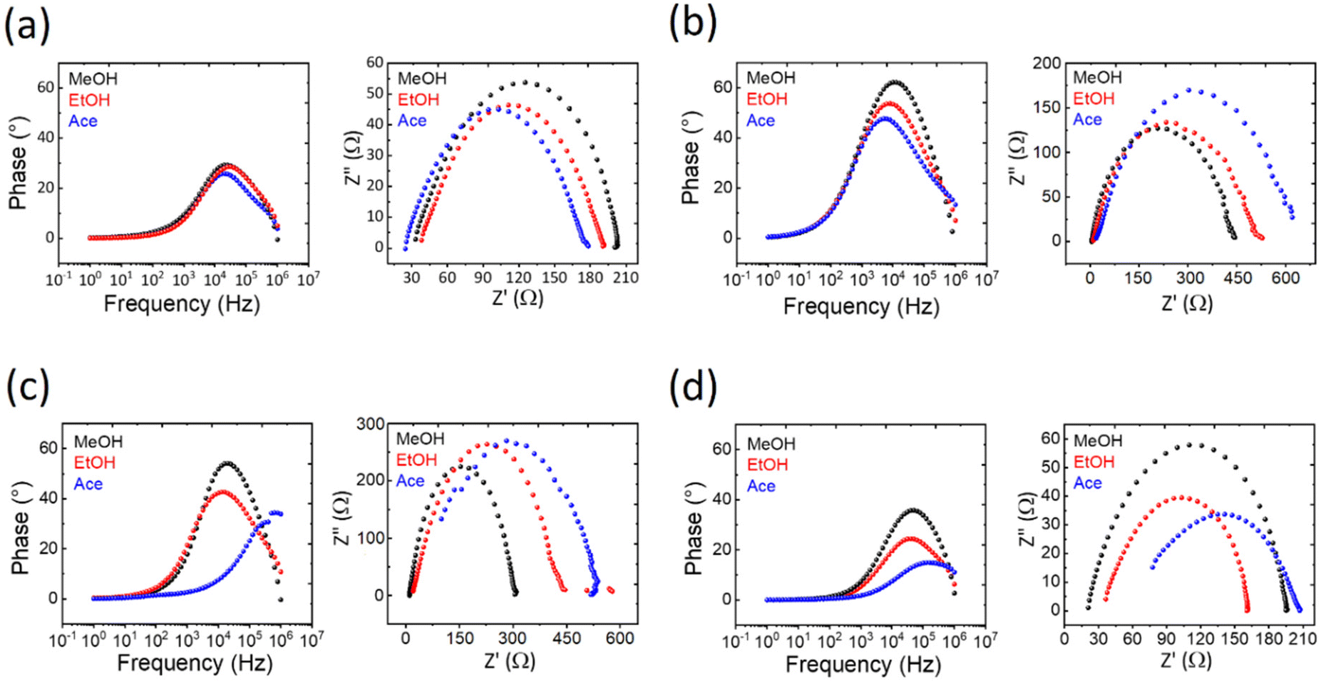 | ||
| Fig. 8 Impedance phase spectra and Nyquist plots of the (a) pristine few-layered Ti3C2Tx MXene, (b) Te/Ti3C2Tx, (c) Se/Ti3C2Tx, and (d) S/Ti3C2Tx vapor sensors with methanol (MeOH), ethanol (EtOH) and acetone organic vapors. | ||
4. Conclusions
MXenes have great potential to be used in a range of energy storage and energy conversion devices since they provide remarkable promise as photo(electro)catalysts. However, their efficiencies are yet to be developed with a few additional possible components and routes. As a result, some potential chalcogen elements of Te, Se, and S were selected and successfully anchored on the few-layered Ti3C2Tx by a facile solid-state chemistry annealing technique. PEC photodetector, HER, and vapor sensor analyses revealed that the chalcogen decorated few-layered Ti3C2Tx composite has a greater impact on the efficiencies of such systems than the pristine few-layered Ti3C2Tx MXene. Occupation of pristine Ti3C2Tx MXene defects and optical bandgap reduction by the chalcogen element decoration are two reasons for the enhancement of the photodetector activity of the chalcogen decorated Ti3C2Tx MXene composite samples. Moreover, it was analyzed that the photocurrent density, photoresponsivity, and detectivity of Te/Ti3C2Tx are higher than those of the other Se/Ti3C2Tx and S/Ti3C2Tx samples. This variation was due to the lower ionization energy of the Te in comparison with the other Se and S elements. Thus, the Te/Ti3C2Tx sample could transfer the separated electrons to the electrode system in the PEC photodetector more quickly and efficiently. The evaluation of the HER in the chalcogen decorated few-layered Ti3C2Tx composite samples also showed an enhancement in the production of H2 due to the largeO contents and non-stoichiometric formation phases on the surface of the Ti3C2Tx MXene after modification. These two attributes could generate active sites to raise the H+/e− coupling reaction rate and form greater H2. Furthermore, the reduced –F, higher O, rich d-electron of chalcogen elements, and non-stoichiometric formed phases, all could boost electrons on the surface of the chalcogen decorated few-layered Ti3C2Tx MXene composite samples, and subsequently, interactions by the methanol, ethanol, and acetone polar molecules with result in a larger charge transfer and vapor sensing. This work indicates an effective synthesis strategy in developing efficient materials for state-of-the-art applications and can provide new visions into the advancement of the other MXene-based family members that can be employed in high-performance energy systems.
Conflicts of interest
There are no conflicts to declare.Acknowledgements
J. A. was supported by the European Structural and Investment Funds, OP RDE-funded project ‘CHEMFELLS IV’ (No. CZ.02.2.69/0.0/0.0/20_079/0017899). This project was supported by Czech Science Foundation (GACR No. 20-16124J).References
- X. Zhang, A. Chen, L. Chen and Z. Zhou, Adv. Energy Mater., 2022, 12, 2003841 CrossRef CAS.
- S. Khan, A. Khan, J. Azadmanjiri, P. Kumar Roy, L. Děkanovský, Z. Sofer and A. Numan, Adv. Photonics Res., 2022, 3, 2100342 CrossRef.
- A. Khan, J. Azadmanjiri, B. Wu, L. Liping, Z. Sofer and J. Min, Adv. Energy Mater., 2021, 11, 2100451 CrossRef CAS.
- J. Zha, M. Luo, M. Ye, T. Ahmed, X. Yu, D.-H. Lien, Q. He, D. Lei, J. C. Ho, J. Bullock, K. B. Crozier and C. Tan, Adv. Funct. Mater., 2022, 32, 2111970 CrossRef CAS.
- J. Azadmanjiri, V. K. Srivastava, P. Kumar, J. Wang and A. Yu, J. Mater. Chem. A, 2018, 6, 13509–13537 RSC.
- P. K. Roy, N. Antonatos, T. Li, Y. Jing, J. Luxa, J. Azadmanjiri, P. Marvan, T. Heine and Z. Sofer, ACS Appl. Mater. Interfaces, 2023, 15(1), 1859–1870 CrossRef CAS PubMed.
- M. Turunen, M. Brotons-Gisbert, Y. Dai, Y. Wang, E. Scerri, C. Bonato, K. D. Jöns, Z. Sun and B. D. Gerardot, Nat. Rev. Phys., 2022, 4, 219–236 CrossRef.
- J. Azadmanjiri, V. K. Srivastava, P. Kumar, Z. Sofer, J. Min and J. Gong, Appl. Mater. Today, 2020, 19, 100600 CrossRef.
- S. Wei, S. Mourdikoudis, B. Wu, J. Pastika, R. Gusmão, J. Azadmanjiri, L. Dekanovsky, J. Luxa, M. Li and V. Mazánek, 2D Mater., 2022, 9, 045032 CrossRef.
- D. Zhao, Z. Chen, W. Yang, S. Liu, X. Zhang, Y. Yu, W.-C. Cheong, L. Zheng, F. Ren, G. Ying, X. Cao, D. Wang, Q. Peng, G. Wang and C. Chen, J. Am. Chem. Soc., 2019, 141, 4086–4093 CrossRef CAS PubMed.
- J. Zou, J. Wu, Y. Wang, F. Deng, J. Jiang, Y. Zhang, S. Liu, N. Li, H. Zhang, J. Yu, T. Zhai and H. N. Alshareef, Chem. Soc. Rev., 2022, 51, 2972–2990 RSC.
- Y. Wang, T. Guo, Z. Tian, K. Bibi, Y.-Z. Zhang and H. N. Alshareef, Adv. Mater., 2022, 34, 2108560 CrossRef CAS PubMed.
- M. Zhang, C. Lai, B. Li, S. Liu, D. Huang, F. Xu, X. Liu, L. Qin, Y. Fu, L. Li, H. Yi and L. Chen, Small, 2021, 17, 2007113 CrossRef CAS PubMed.
- A. Al-Temimy, B. Anasori, K. A. Mazzio, F. Kronast, M. Seredych, N. Kurra, M.-A. Mawass, S. Raoux, Y. Gogotsi and T. Petit, J. Phys. Chem. C, 2020, 124, 5079–5086 CrossRef CAS.
- J. Xia, S.-Z. Yang, B. Wang, P. Wu, I. Popovs, H. Li, S. Irle, S. Dai and H. Zhu, Nano Energy, 2020, 72, 104681 CrossRef CAS.
- L. Děkanovský, J. Azadmanjiri, M. Havlík, P. Bhupender, J. Šturala, V. Mazánek, A. Michalcová, L. Zeng, E. Olsson, B. Khezri and Z. Sofer, Small Methods, 2022, 2201329 CrossRef PubMed.
- L. Gao, W. Bao, A. V. Kuklin, S. Mei, H. Zhang and H. Ågren, Adv. Mater., 2021, 33, 2004129 CrossRef CAS PubMed.
- M. Shekhirev, J. Busa, C. E. Shuck, A. Torres, S. Bagheri, A. Sinitskii and Y. Gogotsi, ACS Nano, 2022, 16(9), 13695–13703 CrossRef CAS PubMed.
- K. R. G. Lim, M. Shekhirev, B. C. Wyatt, B. Anasori, Y. Gogotsi and Z. W. Seh, Nat. Synth., 2022, 1, 601–614 CrossRef.
- L. H. Karlsson, J. Birch, J. Halim, M. W. Barsoum and P. O. Å. Persson, Nano Lett., 2015, 15, 4955–4960 CrossRef CAS PubMed.
- J. Azadmanjiri, T. N. Reddy, B. Khezri, L. Děkanovský, A. K. Parameswaran, B. Pal, S. Ashtiani, S. Wei and Z. Sofer, J. Mater. Chem. A, 2022, 10, 4533–4557 RSC.
- C. Zhang, Y. Ma, X. Zhang, S. Abdolhosseinzadeh, H. Sheng, W. Lan, A. Pakdel, J. Heier and F. Nüesch, Energy Environ. Mater., 2020, 3, 29–55 CrossRef CAS.
- A. Bafekry, C. V. Nguyen, C. Stampfl, B. Akgenc and M. Ghergherehchi, Phys. Status Solidi B, 2020, 257, 2000343 CrossRef CAS.
- X. Li, X. Lv, X. Sun, C. Yang, Y.-Z. Zheng, L. Yang, S. Li and X. Tao, Appl. Catal., B, 2021, 284, 119708 CrossRef CAS.
- X. Wu, Z. Wang, M. Yu, L. Xiu and J. Qiu, Adv. Mater., 2017, 29, 1607017 CrossRef PubMed.
- D. Zhao, P. Wang, H. Di, P. Zhang, X. Hui and L. Yin, Adv. Funct. Mater., 2021, 31, 2010544 CrossRef CAS.
- J. Yao and G. Yang, Adv. Sci., 2022, 9, 2103036 CrossRef PubMed.
- J. Azadmanjiri, L. Děkanovský, S. Wei, M. Li and Z. Sofer, J. Energy Storage, 2022, 56, 105918 CrossRef.
- H. L. Chia, C. C. Mayorga-Martinez, N. Antonatos, Z. Sofer, J. J. Gonzalez-Julian, R. D. Webster and M. Pumera, Anal. Chem., 2020, 92, 2452–2459 CrossRef CAS PubMed.
- M. Seredych, C. E. Shuck, D. Pinto, M. Alhabeb, E. Precetti, G. Deysher, B. Anasori, N. Kurra and Y. Gogotsi, Chem. Mater., 2019, 31, 3324–3332 CrossRef CAS.
- W.-J. Ong, L.-L. Tan, S.-P. Chai, S.-T. Yong and A. R. Mohamed, Nanoscale, 2014, 6, 1946–2008 RSC.
- M. Naguib, O. Mashtalir, M. R. Lukatskaya, B. Dyatkin, C. Zhang, V. Presser, Y. Gogotsi and M. W. Barsoum, Chem. Commun., 2014, 50, 7420–7423 RSC.
- J. Azadmanjiri, P. K. Roy, L. Děkanovský, J. Regner and Z. Sofer, 2D Mater., 2022, 9, 045019 CrossRef.
- L. Zheng, S. Han, H. Liu, P. Yu and X. Fang, Small, 2016, 12, 1527–1536 CrossRef CAS PubMed.
- C. Peng, P. Wei, X. Li, Y. Liu, Y. Cao, H. Wang, H. Yu, F. Peng, L. Zhang, B. Zhang and K. Lv, Nano Energy, 2018, 53, 97–107 CrossRef CAS.
- M. Long, A. Gao, P. Wang, H. Xia, C. Ott, C. Pan, Y. Fu, E. Liu, X. Chen, W. Lu, T. Nilges, J. Xu, X. Wang, W. Hu and F. Miao, Sci. Adv., 2017, 3, e1700589 CrossRef PubMed.
- P. K. Roy, P. Marvan, V. Mazánek, N. Antonatos, D. Bouša, E. Kovalska, D. Sedmidubský and Z. Sofer, ACS Appl. Mater. Interfaces, 2021, 13, 30806–30817 CrossRef CAS PubMed.
- U. Bockelmann, P. Hiergeist, G. Abstreiter, G. Weimann and W. Schlapp, Surf. Sci., 1990, 229, 398–401 CrossRef CAS.
- P. Schwerdtfeger and J. K. Nagle, Mol. Phys., 2019, 117, 1200–1225 CrossRef CAS.
- T. S. Walmsley and Y.-Q. Xu, Nanoscale, 2021, 13, 11836–11843 RSC.
- A. P. Murthy, J. Theerthagiri, J. Madhavan and K. Murugan, Phys. Chem. Chem. Phys., 2017, 19, 1988–1998 RSC.
- A. P. Murthy, J. Theerthagiri and J. Madhavan, J. Phys. Chem. C, 2018, 122, 23943–23949 CrossRef CAS.
- H. Prats and K. Chan, Phys. Chem. Chem. Phys., 2021, 23, 27150–27158 RSC.
- D. Johnson, H.-E. Lai, K. Hansen, P. B. Balbuena and A. Djire, Nanoscale, 2022, 14, 5068–5078 RSC.
- E. Mitterreiter, B. Schuler, A. Micevic, D. Hernangómez-Pérez, K. Barthelmi, K. A. Cochrane, J. Kiemle, F. Sigger, J. Klein, E. Wong, E. S. Barnard, K. Watanabe, T. Taniguchi, M. Lorke, F. Jahnke, J. J. Finley, A. M. Schwartzberg, D. Y. Qiu, S. Refaely-Abramson, A. W. Holleitner, A. Weber-Bargioni and C. Kastl, Nat. Commun., 2021, 12, 3822 CrossRef CAS PubMed.
- Y. Liu, P. Stradins and S.-H. Wei, Angew. Chem., Int. Ed., 2016, 55, 965–968 CrossRef CAS PubMed.
- K. Hu, L.-M. Guan, D. Han, F. Liu and S.-Y. Xie, J. Phys. Chem. Lett., 2021, 12, 9422–9428 CrossRef CAS PubMed.
- H. Li, C. Tsai, A. L. Koh, L. Cai, A. W. Contryman, A. H. Fragapane, J. Zhao, H. S. Han, H. C. Manoharan, F. Abild-Pedersen, J. K. Nørskov and X. Zheng, Nat. Mater., 2016, 15, 48–53 CrossRef CAS PubMed.
- H. Shu, D. Zhou, F. Li, D. Cao and X. Chen, ACS Appl. Mater. Interfaces, 2017, 9, 42688–42698 CrossRef CAS PubMed.
- Y. S. Chang, C. Y. Chen, C. J. Ho, C. M. Cheng, H. R. Chen, T. Y. Fu, Y. T. Huang, S. W. Ke, H. Y. Du, K. Y. Lee, L. C. Chao, L. C. Chen, K. H. Chen, Y. W. Chu and R. S. Chen, Nano Energy, 2021, 84, 105922 CrossRef CAS.
- M. Wang, Z. Sun, H. Ci, Z. Shi, L. Shen, C. Wei, Y. Ding, X. Yang and J. Sun, Angew. Chem., Int. Ed., 2021, 60, 24558–24565 CrossRef CAS PubMed.
- S. M. Majhi, A. Ali, Y. E. Greish, H. F. El-Maghraby, N. N. Qamhieh, A. R. Hajamohideen and S. T. Mahmoud, ACS Appl. Electron. Mater., 2022, 4(8), 4094–4103 CrossRef CAS.
- J. Lee, Y. C. Kang, C. M. Koo and S. J. Kim, ACS Appl. Nano Mater., 2022, 5(8), 11997–12005 CrossRef CAS.
- J. Choi, B. Chacon, H. Park, K. Hantanasirisakul, T. Kim, K. Shevchuk, J. Lee, H. Kang, S.-Y. Cho, J. Kim, Y. Gogotsi, S. J. Kim and H.-T. Jung, ACS Sens., 2022, 7(8), 2225–2234 CrossRef CAS PubMed.
- S. Mehdi Aghaei, A. Aasi and B. Panchapakesan, ACS Omega, 2021, 6, 2450–2461 CrossRef CAS PubMed.
- R. Bhardwaj and A. Hazra, J. Mater. Chem. C, 2021, 9, 15735–15754 RSC.
- X. Mettan, J. Jaćimović, O. S. Barišić, A. Pisoni, I. Batistić, E. Horváth, S. Brown, L. Rossi, P. Szirmai, B. Farkas, H. Berger and L. Forró, Commun. Phys., 2019, 2, 123 CrossRef.
Footnote |
| † Electronic supplementary information (ESI) available. See DOI: https://doi.org/10.1039/d2nr05730a |
| This journal is © The Royal Society of Chemistry 2023 |