
 Open Access Article
 This Open Access Article is licensed under a Creative Commons Attribution-Non Commercial 3.0 Unported Licence
High throughput processing of dinaphtho[2,3-b:2′,3′-f]thieno[3,2-b]thiophene (DNTT) organic semiconductors†
Lamiaa
Fijahi‡
 a,
Jinghai
Li‡
a,
Adrián
Tamayo
a,
Martina
Volpi
b,
Guillaume
Schweicher
b,
Yves H.
Geerts
bc and
Marta
Mas-Torrent
*a
a,
Jinghai
Li‡
a,
Adrián
Tamayo
a,
Martina
Volpi
b,
Guillaume
Schweicher
b,
Yves H.
Geerts
bc and
Marta
Mas-Torrent
*a
aInstitut de Ciència de Materials de Barcelona (ICMAB-CSIC), Campus de la UAB, 08193 Bellaterra, Barcelona, Spain. E-mail: mmas@icmab.es
bLaboratoire de Chimie des Polymères, Faculté des Sciences, Université Libre de Bruxelles (ULB), Boulevard du Triomphe, CP 206/01, 1050 Bruxelles, Belgium
cInternational Solvay Institutes for Physics and Chemistry, Université Libre de Bruxelles (ULB), Boulevard du Triomphe, CP 231, 1050 Bruxelles, Belgium
First published on 16th November 2022
Abstract
The deposition of organic semiconductors (OSCs) using solution shearing deposition techniques is highly appealing for device implementation. However, when using high deposition speeds, it is necessary to use very concentrated OSC solutions. The OSCs based on the family of dinaphtho[2,3-b:2′,3′-f]thieno[3,2-b]thiophene (DNTT) have been shown to be excellent OSCs due to their high mobility and stability. However, their limited solubility hinders the processing of these materials at high speed. Here, we report the conditions to process alkylated DNTT and the S-shaped π-core derivative S-DNTT by bar-assisted meniscus shearing (BAMS) at high speed (i.e., 10 mm s−1). In all the cases, homogeneous thin films were successfully prepared, although we found that the gain in solubility achieved with the S-DNTT derivative strongly facilitated solution processing, achieving a field-effect mobility of 2.1 cm2 V−1 s−1, which is two orders of magnitude higher than the mobility found for the less soluble linear derivatives.
Introduction
Organic semiconductors (OSCs) have received a great deal of attention over the last decades due to their potential use in printed electronics. In contrast to conventional electronics, organic electronics is appealing to emerging applications in which low-cost, large-area coverage and flexibility are required. For this purpose, developing solution printing techniques capable of processing OSCs that exhibit high electrical performance is key.1–3Among the different solution-based processing techniques, the use of solution-shearing techniques to prepare thin films of OSCs is currently of high interest.1,4–8 Solution shearing deposition can be performed over larger areas, is compatible with roll-to-roll processes and can potentially be realised at high throughput. However, the deposition of small-molecule OSCs by solution shearing, especially at high coating speeds, also faces fundamental challenges. Small-molecule OSCs tend to suffer from dewetting issues leading to non-homogeneous films. This can be often overcome by using more viscous inks based on blends of OSCs and insulating polymers.9–18 Furthermore, the use of blends has also often been shown to give rise to more crystalline films exhibiting lower interfacial traps thanks to the passivation of the dielectric by the binding polymer.19 In addition, the solubility of the OSC is crucial to being able to process the material by solution shearing. When low deposition rates of the order of 5–100 μm s−1 are applied, such as for instance with the zone casting technique,20–22 it is possible to use solutions with OSC concentrations of around 0.2–2 mg mL−1. However, when the OSC thin films are prepared at higher deposition speeds (i.e., >5 mm s−1), typically the solubility of the OSC needs to be much higher, i.e., 10–20 mg mL−1.15,23,24 Again, the use of blends can also help by reducing the required amount of solubilised OSC, commonly by around a factor of 25–50% depending on the OSC![[thin space (1/6-em)]](https://www.rsc.org/images/entities/char_2009.gif) :polymer ratio used.
:polymer ratio used.
Dinaphtho[2,3-b:2′,3′-f]thieno[3,2-b]thiophene (DNTT, Fig. 1a)25–29 derivatives are currently considered benchmark OSCs since they exhibit high mobility in organic field-effect transistors (OFETs) and good environmental stability. Due to the poor solubility of the parent DNTT compound, different derivatives have been synthesised in order to achieve better solubility and afford the processability of these materials from solution. One route that has been pursued is the use of soluble precursors that, after heating, convert to DNTT.30,31 Alternatively, DNTT derivatives bearing long alkyl groups or one branched alkyl group have been synthesised with the aim of enhancing the intermolecular interactions between the semiconducting cores while improving their solubility in common organic solvents.32–35 Unfortunately, the resulting alkylated derivatives still show limited solubility, making it difficult to print them when employing high throughput techniques. Only a few works have reported the solution deposition of alkylated DNTT derivatives for the fabrication of thin film OFETs, in which spin-coating,33,36 solution confinement37 or a low-rate solution shearing technique was employed.38–40 The OFETs based on these films exhibited mobility values in the range of 0.1–1 cm2 V−1 s−1 for spin-coated films, and around 10 cm2 V−1 s−1 for films prepared by solution shearing or solution confinement. Recently, new DNTT derivatives were reported featuring an S-shaped sinuous π-core (i.e., S-DNTT) and substituted with long alkyl chains.41 The modification of the π-core from a linear to a crooked shape improved the material solubility in common organic solvents by around 30 times (i.e., from ∼0.12 mmol L−1 for C10-DNTT to 3.7 mmol L−1 for S-DNTT-10 in toluene at 60 °C).41 OFETs with a high hole mobility of up to 11 cm2 V−1 s−1 were reported with these derivatives after depositing them by dip-coating at a low coating speed of 4 μm s−1. Thus, despite their excellent electrical properties, the fabrication of DNTT-based OFETs using high throughput printing techniques has been hardly explored mainly due to their limited solubility in organic solvents.
 | ||
| Fig. 1 (a) Molecular structures of the used organic semiconductors and binder polymer. (b) Schematic illustration of the BAMS technique and the top-contact bottom-gate OFET architecture. | ||
In this work, we investigated the potential of alkylated DNTT and S-DNTT derivatives to be processed by the bar-assisted meniscus shearing (BAMS)17,23,42,43 technique at high speed (i.e., 10 mm s−1). The use of blends of these materials with polystyrene (PS) has also been explored as a route to facilitate the preparation of homogeneous thin films. In all cases, we succeeded in preparing homogeneous thin films, although we found that the gain in solubility achieved with the S-DNTT derivative strongly facilitated solution processing. An average field-effect mobility of 1.7 cm2 V−1 s−1 was recorded for the alkylated S-DNTT OSC, which was further improved up to 2.1 cm2 V−1 s−1 after doping the films in order to reduce the contact resistance. Therefore, this work proves that, with appropriate molecular modifications, DNTT materials are OSCs of high potential for the fabrication of large-area printed devices.
Results and discussion
The soluble DNTT OSCs 2,9-dioctylnaphtho[2,3-b]naphtha [2′,3′:4,5]thieno[2,3-d]thiophene (C8-DNTT), 2,9-didecyldinaphtho[2,3-b:2′,3′-f]thieno[3,2-b]thiophene (C10-DNTT) and 3,10-didecylnaphtho[2,1-b]naphtha[1′,2′:4,5] thieno[2,3-d]thiophene (S-DNTT-10) were selected for processing using the bar-assisted meniscus shearing (BAMS) technique (Fig. 1). This technique has previously been applied for the deposition of benchmark soluble OSCs realizing highly crystalline and reproducible films at high throughput.17,23,42,44 It consists of pouring an OSC solution in between a hot-plate and a bar separated ∼500 μm apart forming a confined meniscus and, subsequently, the substrate is displaced in parallel to the bar at a constant speed, typically at 10 mm s−1.Solutions of the DNTT derivatives and the DNTT derivatives blended with polystyrene (PS) at 2 wt% were prepared in chlorobenzene. PS was chosen as the binding polymer due to its low relative permittivity, good solubility in organic solvents, low cost and the fact that it interacts weakly with OSCs. In the case of S-DNTT-10, the prepared solutions were stable even at room temperature. However, with the C10-DNTT and C8-DNTT OSCs, the solutions had to be heated at 120 °C, as otherwise the materials quickly precipitated (Fig. S1†). It was noticed that solutions with lower concentrations were not suitable for deposition at high speed. Different solvents and solvent mixtures were tested but similar solubility issues were encountered. Regarding the blend formulation, the most optimum conditions were found using an OSC:PS ratio of 4:1 with PS of molecular weight 280 kDa.
The deposition of S-DNTT-10 by BAMS was carried out by heating the Si/SiO2 substrate and the corresponding solutions at 105 °C, following previously reported conditions applied to other OSCs. At this temperature, the solvent evaporates simultaneously as the substrate is dragged, reaching an intermediate deposition regime in between the capillary regime and the Landau–Levich regime.45 However, the deposition of C10-DNTT and C8-DNTT was more challenging. When depositing these materials at 105 °C, non-homogeneous films with defects and precipitated small crystals were formed, especially with the shortest alkylated derivative (Fig. S2†). To circumvent this problem, the solution depositions were performed at 120 °C and then, homogeneous films were successfully achieved. It should be highlighted that the deposition process in these cases had to be performed very fast in order to avoid precipitation of the OSCs close to the bar. Subsequently, top-contact gold source–drain electrodes were evaporated through a shadow mask with a constant channel width (W) of 4000 μm and different channel lengths (L) of 35, 80 and 175 μm. In Fig. 1b the final device architecture is illustrated.
The thin film morphology of the three DNTT derivatives was inspected by optical polarised microscopy (Fig. S3†). All films were polycrystalline showing small crystal domains and no preferential orientation. By atomic force microscopy (AFM) characterization, the crystallites were visualized, especially on thin films based on pristine OSCs (Fig. 2). Generally, the films based on Cn-DNTT reveal more pronounced terraces and smaller crystalline domains than the ones of S-DNTT-10. Also, cracks can be observed in the Cn-DNTT films. All this could be caused by the faster crystallization of these materials due to their lower solubility and the higher temperature required for their deposition. The films based on S-DNTT-10, C8-DNTT and C10-DNTT showed step edges of around 39 ± 3, 34 ± 3 and 38 ± 4 Å, respectively, which is in agreement with the length of an extended molecule (insets in Fig. 2). This is also in accordance with our previous results that showed, in blended films prepared by BAMS, that a vertical phase separation occurs in which the OSC crystallises on the top part of the film.19,23,43
 | ||
| Fig. 2 AFM topography images of the films based on OSC and OSC:PS films deposited by BAMS on a SiO2/Si substrate. Scale bar: 2 μm. The insets are the height profiles along the blue lines marked in the images. | ||
The thicknesses of pristine C8-DNTT, C10-DNTT and S-DNTT-10 films were found to be 18.6 ± 3.8, 15.6 ± 6.2, and 24.6 ± 4.7 nm, respectively, with a route mean square roughness (Rrms) of 4.5 ± 2.1, 4.2 ± 1.4, and 4.8 ± 1.4 nm. Further, the C8-DNTT, C10-DNTT and S-DNTT-10 blended films were 17.4 ± 7.7, 16.5 ± 6.1, and 24.9 ± 3.9 nm thick with a Rrms of 4.6 ± 2.2, 5.7 ± 2.4, and 3.2 ± 1.1 nm, respectively.
All the thin films were characterised by X-ray diffraction (XRD) (Fig. 3). All the films were highly crystalline and the crystals were oriented along the surface plane since only the set of (00l) reflections are observed. The XRD data of Cn-DNTT derivatives were in agreement with the previously reported herring-bone crystal structures of these two materials (Table S1†).46,47 In addition, the pattern obtained in S-DNTT-10 films was also in accordance with the surface-induced phase afforded for the reported dip-coated and evaporated films, which were also described to assemble following a herring-bone arrangement.41 It should be noted that this OSC in bulk crystallises with a slipped π-stack motif.41
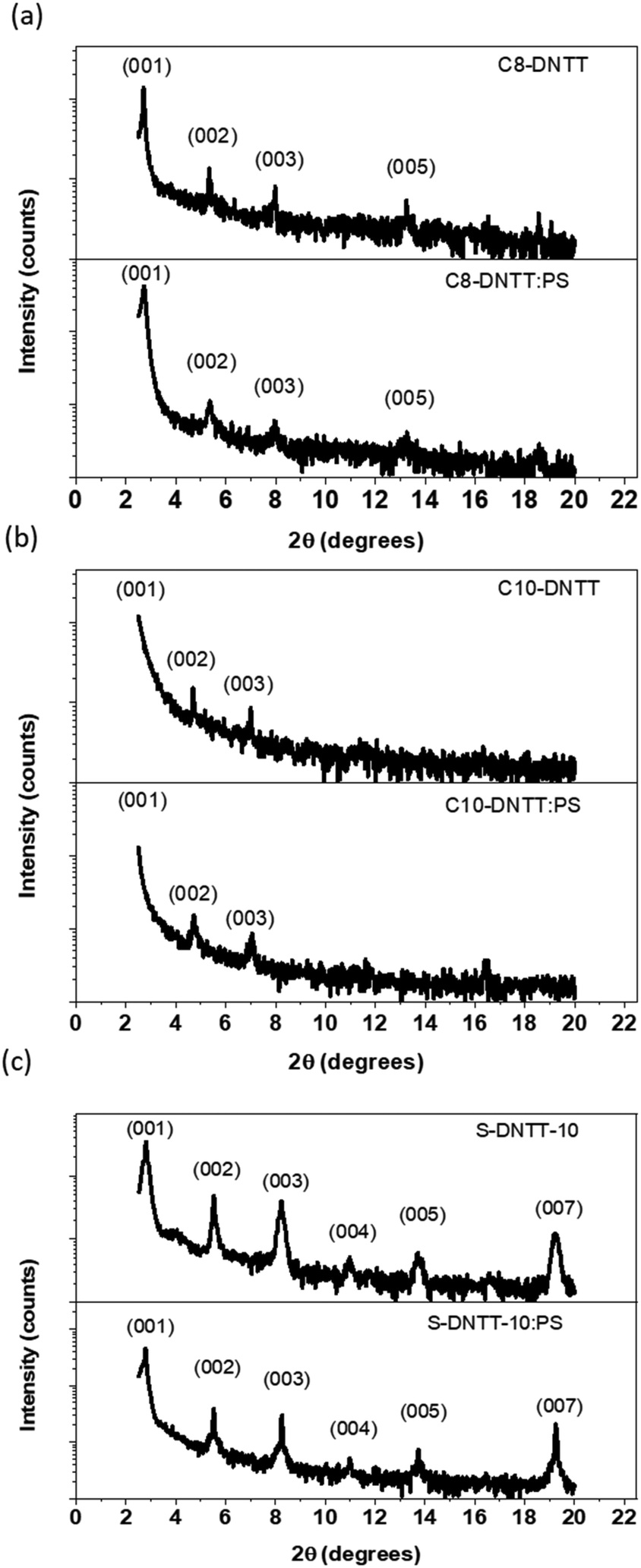 | ||
| Fig. 3 XRD diffractograms of (a) C8-DNTT, (b) C10-DNTT and (c) S-DNTT-10 thin films deposited by BAMS. | ||
From the XRD measurements, the interlayer distances (d001) were estimated to be 33.4, 37.4 and 31.5 Å for C8-DNTT, C10-DNTT and S-DNTT-10, respectively (Table S2†). These values indicate that the molecules are oriented with the longer axis normal to the substrate but with a certain degree of inclination (θtilt). It was found that while C8-DNTT and C10-DNTT reveal small θtilt values of approximately 11° and 16°, respectively, S-DNTT-10 is inclined 36° with respect to the surface normal. Thus, a smaller θtilt will imply that the molecules are positioned more cofacially, which generally provides an enhancement of the effective π-orbital overlap between neighbouring molecules, thereby improving the charge transport efficiency.41,48,49
The top-contact bottom-gated OFET devices based on pristine DNTT and DNTT derivatives blended with polystyrene were electrically characterized as active layers in OFETs under ambient conditions. Fig. 4 shows the output and transfer characteristics in the saturation regime of a C10-DNTT OFET as representative of the devices based on linear Cn-DNTT OSCs (see Fig. S4† for C8-DNTT OFETs). As expected, all the devices exhibited p-type OFET behaviour. From the output characteristics, some injection problems can be noticed since the IDS/VDS curves show some S-shape patterns at low voltage. The OFETs based on pristine C8-DNTT and C10-DNTT exhibited a similar average mobility (μ) of (4.7 ± 1.6) × 10−2 and (4.2 ± 1.2) × 10−2 cm2 V−1 s−1 and a threshold voltage (VTH) of −10.1 ± 4.3 and −11.0 ± 1.8 V, respectively. The devices based on blends of these materials showed mobility values of the same order but lower VTH (i.e., C8-DNTT:PS:μ = (2.0 ± 0.4) × 10−2 cm2 V−1 s−1 and VTH = 0.1 ± 0.3 V; C10-DNTT:PS: μ = (4.3 ± 0.3) × 10−2 cm2 V−1 s−1 and VTH = −2.2 ± 0.9 V). It should be noted that for the calculation of all the mobility values of the blends in this work, the capacitance of SiO2 has been used. We previously demonstrated that if the total capacitance is considered as a series of the SiO2 and PS capacitances, the calculated mobility values would be around 20% higher.50 Additionally, the hysteresis of the output curves is also reduced in the blends. Thus, this points out that PS improves the organic semiconductor/dielectric interface by reducing charge trapping.
 | ||
| Fig. 4 Transfer (a) and (b) and output (c) and (d) characteristics of OFETs based on C10-DNTT and C10-DNTT:PS films. | ||
The electrical characteristics of S-DNTT-10 films are shown in Fig. 5. The output characteristics of both the pristine semiconductor and the blend show no hysteresis and linearity at low applied voltages. Remarkably, S-DNTT-10 films revealed a mobility of almost two orders of magnitude higher than the films based on the linear Cn-DNTT derivatives, with an average mobility of 1.7 ± 0.6 cm2 V−1 s−1 and a VTH of −5.0 ± 0.8 V. This might be mainly due to the more homogeneous films with larger crystalline domains obtained with this semiconductor. Furthermore, the S-DNTT-10:PS blended films gave rise to an average mobility of 0.4 ± 0.2 cm2 V−1·s−1 and a VTH of 5.8 ± 0.4 V. Hence, contrary to what has been typically observed with other OSCs,17,19,23,51 here the PS does not improve the electrical performance of these films.
 | ||
| Fig. 5 Transfer (a) and (b) and output (c) and (d) characteristics of OFETs based on S-DNTT-10 and S-DNTT-10:PS films. | ||
Considering the high OFET performance of the S-DNTT-10 films, we proceeded to analyse the device mobility dependence in the saturation regime on the channel length. It should be noted that all previous mobility values given were averaged values among devices of different channel lengths (i.e., L = 35, 80 and 175 μm). However, as can be observed in Fig. 6, the devices with a shorter channel length show lower OFET mobility than those with longer L. This is commonly found in devices that exhibit significant contact resistance (RC). At low L, RC has a strong impact on the device performance since channel and contact resistance are more comparable, whereas at higher L, RC becomes more negligible. Recently, it was reported that the treatment of OSC films with aqueous iodine solution resulted in a reduction in RC, improving the effective device mobility.52 Accordingly, we doped the S-DNTT-10 films following the same methodology (see Experimental section) and we explored again the performance of the OFETs of different L. In Fig. S5† representative transfer characteristics of devices before and after doping are shown. It can be clearly observed that after doping, the source–drain current increases and the transfer curves are shifted towards positive voltage values. Remarkably, this doping procedure led to an enhancement of the device mobility, which further became less channel-length dependent, with a shift of the threshold voltage towards 0 V (Fig. 6). These results are in agreement with the improvement of the contact efficiency. Interestingly, the doped S-DNTT-10 devices exhibited an average mobility of 2.1 ± 0.2 cm2 V−1 s−1.
 | ||
| Fig. 6 (a) Saturation mobility and (b) threshold voltage for OFETs based on S-DNTT-10 before (black) and after (red) doping. Each point on the plot represents the mean value and the error bar corresponds to the standard deviation of the data. | ||
Experimental section
Materials and methods
C8-DNTT and C10-DNTT were synthesized as previously described.53 S-DNTT-10 was purchased from TCI and used as received. Iodine solid, polystyrene (PS) of 280 kDa and 2,3,4,5,6-pentafluorothiophenol (PFBT) were purchased from Sigma-Aldrich and used without further purification. Chlorobenzene of high quality was purchased from Aldrich.Transistor fabrication and characterization
Inks based on DNTT derivatives and DNTT derivatives blended with 2 wt% PS in chlorobenzene were prepared. In the case of the blends, a weight ratio OSC:PS of 4:1 was used. The blended films were deposited by a BAMS technique under ambient conditions at 105 °C for S-DNTT-10 and at 120 °C in the case of C8-DNTT and C10-DNTT. The deposition was performed at a coating speed of 10 mm s−1.17,23,42,54
Si/SiO2 substrates were purchased from Si-Mat (SiO2 thickness of 200 nm, C = 17.26 × 10⁻⁹ F cm−2) and were cleaned with acetone and isopropanol and dried under nitrogen flow. Top-contact source–drain electrodes comprising a 25 nm thick layer of Au were thermally evaporated (evaporation rate 0.5 Å s−1) through a shadow mask with a channel width W = 4 mm and channel lengths L = 35, 80 and 175 μm. After evaporation, samples were kept in the dark for 7 days.
Transistor measurements were carried out with an Agilent B1500A semiconductor device analyzer under ambient conditions. The devices were characterized by extracting the field–effect mobility in the saturation regime as follows:

Doping procedure
Doping treatment was done by exposing the top surface of the devices to an aqueous iodine solution (2.9 mg mL−1). A droplet of the OSC solution was cast on the device, covering completely the OFET channel. After 3 min, the device was abundantly washed with MilliQ water and dried under a nitrogen flow.Structural and morphological thin film characterizations
Polarized optical microscopy images were taken and dark field microscopy was performed using an Olympus BX51. The X-ray diffraction measurements were carried out with a Siemens D-5000 model diffractometer that used Cu K-alpha radiation 1.540560 Å. Surface topography and phase and thin film thicknesses were examined using a 5500LS SPM system from Agilent Technologies and subsequent data analysis was performed using Gwyddion 2.56 software.Conclusions
To sum up, the printing of high mobility small-molecule OSCs using high throughput techniques requires highly concentrated solutions in order to afford highly homogeneous and crystalline thin films. DNTT derivatives have been shown to be excellent OSCs due to their high mobility and environmental stability. However, due to their limited solubility in organic solvents, processing these materials at high speed is extremely challenging.Here, we showed that linear DNTT derivatives functionalised with long alkyl chains can be processed at a high coating rate using a BAMS technique under high temperatures and with certain precautions. However, the films reveal the formation of many incomplete molecular layers and some cracks, which have a detrimental impact on the device mobility. Mobility values in the order of 0.04 cm2 V−1 s−1 were achieved. Notably, the devices based on blends of these linear DNTT derivatives with PS showed reduced hysteresis and lower threshold voltages.
Furthermore, the preparation of S-DNTT-10 thin films by BAMS was simpler due to the higher solubility of this material and the fact that it was possible to apply lower coating temperatures. As a result, more homogeneous films were achieved, which led to the production of OFETs presenting mobility values two orders of magnitude higher than those obtained with the lower solubility derivatives.
Therefore, this work demonstrates that DNTT derivatives are highly potential materials for their practical implementation in printed devices and, furthermore, that the modification of the π-core shape is a promising route to improve OSC solubility and, hence, processability.
Conflicts of interest
There are no conflicts to declare.Acknowledgements
This work was funded by the European Union's Horizon 2020 research and innovation programme under the Marie Skłodowska-Curie grant agreement No 811284 (UHMob), the Spanish Ministry (project GENESIS PID2019-111682RB-I00 and through the “Severo Ochoa” Programme for Centers of Excellence in R&D (FUNFUTURE CEX2019-000917-S)) and the Generalitat de Catalunya (2017-SGR-918). L. F. and J. L. are enrolled in the UAB Materials Science PhD program. J. L. acknowledges the Scholarship from the Chinese Council. G. S. is a FNRS research associate (Belgian National Fund for Scientific Research). G. S. acknowledges financial support from the Francqui Foundation (Francqui Start-Up Grant). Y. H. G. is thankful to FNRS for financial support through research projects Pi-Fast (No T.0072.18), Pi-Chir (No T.0094.22), and DIFFRA (No U.G001.19).References
- Y. Diao, L. Shaw, Z. Bao and S. C. B. Mannsfeld, Energy Environ. Sci., 2014, 7, 2145–2159 RSC
.
- S. Park, G. Giri, L. Shaw, G. Pitner, J. Ha, J. H. Koo, X. Gu, J. Park, T. H. Lee, J. H. Nam, Y. Hong and Z. Bao, Proc. Natl. Acad. Sci. U. S. A., 2015, 112, 5561–5566 CrossRef CAS PubMed
- M. Mas-Torrent and C. Rovira, Chem. Soc. Rev., 2008, 37, 827–838 RSC
- S. Riera-Galindo, A. Tamayo and M. Mas-Torrent, ACS Omega, 2018, 3, 2329–2339 CrossRef CAS PubMed
- Y. Xu, C. Liu, D. Khim and Y. Y. Noh, Phys. Chem. Chem. Phys., 2015, 17, 26553–26574 RSC
- G. Giri, E. Verploegen, S. C. B. Mannsfeld, S. Atahan-Evrenk, D. H. Kim, S. Y. Lee, H. A. Becerril, A. Aspuru-Guzik, M. F. Toney and Z. Bao, Nature, 2011, 480, 504–508 CrossRef CAS PubMed
- X. Gu, L. Shaw, K. Gu, M. F. Toney and Z. Bao, Nat. Commun., 2018, 9, 534 CrossRef
- J. J. Michels, K. Zhang, P. Wucher, P. M. Beaujuge, W. Pisula and T. Marszalek, Nat. Mater., 2021, 20, 68–75 CrossRef CAS PubMed
- S. Riera-Galindo, F. Leonardi, R. Pfattner and M. Mas-Torrent, Adv. Mater. Technol., 2019, 4, 1900104 CrossRef CAS
- J. Smith, R. Hamilton, I. McCulloch, N. Stingelin-Stutzmann, M. Heeney, D. D. C. Bradley and T. D. Anthopoulos, J. Mater. Chem., 2010, 20, 2562–2574 RSC
- W. H. Lee and Y. D. Park, Polymers., 2014, 6, 1057–1073 CrossRef
- L. Janasz, M. Borkowski, P. W. M. Blom, T. Marszalek and W. Pisula, Adv. Funct. Mater., 2021, 2105456 Search PubMed
- Z. Zhang, R. Shi, A. Amini, S. K. So and C. Cheng, Phys. Status Solidi RRL, 2022, 16, 202100602 Search PubMed
- A. F. Paterson, N. D. Treat, W. Zhang, Z. Fei, G. Wyatt-Moon, H. Faber, G. Vourlias, P. A. Patsalas, O. Solomeshch, N. Tessler, M. Heeney and T. D. Anthopoulos, Adv. Mater., 2016, 28, 7791–7798 CrossRef CAS PubMed
- M. R. Niazi, R. Li, E. Q. Li, A. R. Kirmani, M. Abdelsamie, Q. Wang, W. Pan, M. M. Payne, J. E. Anthony, D. M. Smilgies, S. T. Thoroddsen, E. P. Giannelis and A. Amassian, Nat. Commun., 2015, 6, 8598 CrossRef CAS
- A. Tamayo, T. Salzillo and M. Mas-Torrent, Adv. Mater. Interfaces, 2022, 9, 2101679 CrossRef CAS
- T. Salzillo, A. Campos, A. Babuji, R. Santiago, S. T. Bromley, C. Ocal, E. Barrena, R. Jouclas, C. Ruzie, G. Schweicher, Y. H. Geerts and M. Mas-Torrent, Adv. Funct. Mater., 2020, 30, 2006115 CrossRef CAS
- K. Haase, C. Teixeira da Rocha, C. Hauenstein, Y. Zheng, M. Hambsch and S. C. B. Mannsfeld, Adv. Electron. Mater., 2018, 4, 1800076 CrossRef
- A. Campos, S. Riera-Galindo, J. Puigdollers and M. Mas-Torrent, ACS Appl. Mater. Interfaces, 2018, 10, 15952–15961 CrossRef CAS PubMed
- M. Mas-Torrent, S. Masirek, P. Hadley, N. Crivillers, N. S. Oxtoby, P. Reuter, J. Veciana, C. Rovira and A. Tracz, Org. Electron., 2008, 9, 143–148 CrossRef CAS
- W. Pisula, A. Menon, M. Stepputat, I. Lieberwirth, U. Kolb, A. Tracz, H. Sirringhaus, T. Pakula and K. Müllen, Adv. Mater., 2005, 17, 684–689 CrossRef CAS
- P. Miskiewicz, S. Kotarba, J. Jung, T. Marszalek, M. Mas-Torrent, E. Gomar-Nadal, D. B. Amabilino, C. Rovira, J. Veciana, W. Maniukiewicz and J. Ulanski, J. Appl. Phys., 2008, 104, 054509 CrossRef
- I. Temiño, F. G. del Pozo, M. R. Ajayakumar, S. Galindo, J. Puigdollers and M. Mas-Torrent, Adv. Mater. Technol., 2016, 1, 1600090 CrossRef
- G. Giri, S. Park, M. Vosgueritchian, M. M. Shulaker and Z. Bao, Adv. Mater., 2014, 26, 487–493 CrossRef CAS PubMed
- Z. He, D. Shui, H. Siddhartha, M. Chen, D. Zou, G. Kwok, K. Chik, R. Rafael, K. H. Lee, Y. Piao, S. Zhang, X. Cheng, P. Kwok and L. Chan, Adv. Funct. Mater., 2022, 32, 2205129 CrossRef CAS
- R. Jouclas, J. Liu, M. Volpi, L. Silva de Moraes, G. Garbay, N. McIntosh, M. Bardini, V. Lemaur, A. Vercouter, C. Gatsios, F. Modesti, N. Turetta, D. Beljonne, J. Cornil, A. R. Kennedy, N. Koch, P. Erk, P. Samorì, G. Schweicher and Y. H. Geerts, Adv. Sci., 2022, 9, 2105674 CrossRef CAS
- K. Kuribara, H. Wang, N. Uchiyama, K. Fukuda, T. Yokota, U. Zschieschang, C. Jaye, D. Fischer, H. Klauk, T. Yamamoto, K. Takimiya, M. Ikeda, H. Kuwabara, T. Sekitani, Y. L. Loo and T. Someya, Nat. Commun., 2012, 3, 723 CrossRef PubMed
- U. Zschieschang, T. Yamamoto, K. Takimiya, H. Kuwabara, M. Ikeda, T. Sekitani, T. Someya and H. Klauk, Adv. Mater., 2011, 23, 654–658 CrossRef CAS
- T. Yamamoto and K. Takimiya, J. Am. Chem. Soc., 2007, 129, 2224–2225 CrossRef CAS
- A. Hamaguchi, T. Negishi, Y. Kimura, Y. Ikeda, K. Takimiya, S. Z. Bisri, Y. Iwasa and T. Shiro, Adv. Mater., 2015, 27, 6606–6611 CrossRef CAS PubMed
- Y. Kimura, T. Nagase, T. Kobayashi, A. Hamaguchi, Y. Ikeda, T. Shiro, K. Takimiya and H. Naito, Adv. Mater., 2015, 27, 727–732 CrossRef CAS PubMed
- M. J. Kang, I. Doi, H. Mori, E. Miyazaki, K. Takimiya, M. Ikeda and H. Kuwabara, Adv. Mater., 2011, 23, 1222–1225 CrossRef CAS PubMed
- M. Sawamoto, M. J. Kang, E. Miyazaki, H. Sugino, I. Osaka and K. Takimiya, ACS Appl. Mater. Interfaces, 2016, 8, 3810–3824 CrossRef CAS
- K. Kawabata, S. Usui and K. Takimiya, J. Org. Chem., 2020, 85, 195–206 CrossRef CAS PubMed
- M. J. Kang, E. Miyazaki, I. Osaka and K. Takimiya, Jpn. J. Appl. Phys., 2012, 51, 11PD04 CrossRef
- M. Sawamoto, H. Sugino, M. Nakano and K. Takimiya, Org. Electron., 2017, 46, 68–76 CrossRef CAS
- K. Nakayama, Y. Hirose, J. Soeda, M. Yoshizumi, T. Uemura, M. Uno, W. Li, M. J. Kang, M. Yamagishi, Y. Okada, E. Miyazaki, Y. Nakazawa, A. Nakao, K. Takimiya and J. Takeya, Adv. Mater., 2011, 23, 1626–1629 CrossRef CAS PubMed
- B. Peng, K. Cao, A. H. Y. Lau, M. Chen, Y. Lu and P. K. L. Chan, Adv. Mater., 2020, 32, 2002281 CrossRef CAS
- B. Peng, Z. He, M. Chen and P. K. L. Chan, Adv. Funct. Mater., 2022, 32, 2202632 CrossRef CAS
- B. Peng, Z. Wang and P. K. L. Chan, J. Mater. Chem. C, 2016, 4, 8628–8633 RSC
- Y. Yamaguchi, Y. Kojiguchi, S. Kawata, T. Mori, K. Okamoto, M. Tsutsui, T. Koganezawa, H. Katagiri and T. Yasuda, Chem. Mater., 2020, 32, 5350–5360 CrossRef CAS
- F. G. del Pozo, S. Fabiano, R. Pfattner, S. Georgakopoulos, S. Galindo, X. Liu, S. Braun, M. Fahlman, J. Veciana, C. Rovira, X. Crispin, M. Berggren and M. Mas-Torrent, Adv. Funct. Mater., 2016, 26, 2379–2386 CrossRef CAS
- A. Tamayo, I. Fratelli, A. Ciavatti, C. Martínez-Domingo, P. Branchini, E. Colantoni, S. De Rosa, L. Tortora, A. Contillo, R. Santiago, S. T. Bromley, B. Fraboni, M. Mas-Torrent and L. Basiricò, Adv. Electron. Mater., 2022, 8, 2200293 CrossRef CAS
- A. Tamayo, S. Hofer, T. Salzillo, C. Ruzié, G. Schweicher, R. Resel and M. Mas-Torrent, J. Mater. Chem. C, 2021, 9, 7186–7193 RSC
- S. Galindo, A. Tamayo, F. Leonardi and M. Mas-Torrent, Adv. Funct. Mater., 2017, 27, 1700526 CrossRef
- G. Schweicher, G. D'Avino, M. T. Ruggiero, D. J. Harkin, K. Broch, D. Venkateshvaran, G. Liu, A. Richard, C. Ruzié, J. Armstrong, A. R. Kennedy, K. Shankland, K. Takimiya, Y. H. Geerts, J. A. Zeitler, S. Fratini and H. Sirringhaus, Adv. Mater., 2019, 31, 1902407 CrossRef CAS PubMed
- F. Talnack, S. Hutsch, M. Bretschneider, Y. Krupskaya, B. Büchner, M. Malfois, M. Hambsch, F. Ortmann and S. C. B. Mannsfeld, Mol. Syst. Des. Eng., 2022, 7, 507–519 RSC
- A. A. Leitch, A. Mansour, K. A. Stobo, I. Korobkov and J. L. Brusso, Cryst. Growth Des., 2012, 12, 1416–1421 CrossRef CAS
- J. L. Brédas, J. P. Calbert, D. A. Da Silva Filho and J. Cornil, Proc. Natl. Acad. Sci. U. S. A., 2002, 99, 5804–5809 CrossRef
- M. Berteau-Rainville, A. Tamayo, T. Leydecker, A. Pezeshki, E. Orgiu and M. Mas-Torrent, Appl. Phys. Express, 2021, 119, 103301 CAS
- F. Leonardi, S. Casalini, Q. Zhang, S. Galindo, D. Gutiérrez and M. Mas-Torrent, Adv. Mater., 2016, 28, 10311–10316 CrossRef CAS PubMed
- J. Li, A. Babuji, I. Temiño, T. Salzillo, F. D'Amico, R. Pfattner, C. Ocal, E. Barrena and M. Mas-Torrent, Adv. Mater. Technol., 2022, 7, 2101535 CrossRef CAS
- K. Niimi, M. J. Kang, E. Miyazaki, I. Osaka and K. Takimiya, Org. Lett., 2011, 13, 3430–3433 CrossRef CAS PubMed
- L. Fijahi, T. Salzillo, A. Tamayo, M. Bardini, C. Ruzié, C. Quarti, D. Beljonne, S. D'Agostino, Y. Geerts and M. Mas-Torrent, J. Mater. Chem. C, 2022, 10, 7319–7328 RSC
Footnotes |
| † Electronic supplementary information (ESI) available: Additional characterisation data and electrical measurements. See DOI: https://doi.org/10.1039/d2nr05625a |
| ‡ These authors contributed equally to this work. |
| This journal is © The Royal Society of Chemistry 2023 |