
Large-scale controlled coupling of single-photon emitters to high-index dielectric nanoantennas by AFM nanoxerography†
Mélodie
Humbert
ab,
Romain
Hernandez
ab,
Nicolas
Mallet
c,
Guilhem
Larrieu
 c,
Vincent
Larrey
d,
Frank
Fournel
d,
François
Guérin
a,
Etienne
Palleau
a,
Vincent
Paillard
b,
Aurélien
Cuche
b and
Laurence
Ressier
*a
c,
Vincent
Larrey
d,
Frank
Fournel
d,
François
Guérin
a,
Etienne
Palleau
a,
Vincent
Paillard
b,
Aurélien
Cuche
b and
Laurence
Ressier
*a
aUniversité de Toulouse, LPCNO, INSA-UPS-CNRS, 135 avenue de Rangueil, F-31077 Toulouse Cedex 4, France. E-mail: laurence.ressier@insa-toulouse.fr
bCEMES-CNRS, Université de Toulouse, CNRS, UPS, 29 rue Jeanne Marvig, 31055 Toulouse Cedex, France
cLAAS-CNRS, Université de Toulouse, CNRS, UPS, 7 avenue du Colonel Roche BP 54200, 31031 Toulouse Cedex 4, France
dUniversité Grenoble Alpes, CEA, LETI, 17 Avenue des Martyrs, F-38000 Grenoble, France
First published on 9th December 2022
Abstract
Improving the brightness of single-photon sources by means of optically resonant nanoantennas is a major stake for the development of efficient nanodevices for quantum communications. We demonstrate that nanoxerography by atomic force microscopy makes possible the fast, robust and repeatable positioning of model quantum nanoemitters (nitrogen-vacancy NV centers in nanodiamonds) on a large-scale in the gap of silicon nanoantennas with a dimer geometry. By tuning the parameters of the nanoxerography process, we can statistically control the number of deposited nanodiamonds, yielding configurations down to a unique single photon emitter coupled to these high index dielectric nanoantennas, with high selectivity and enhanced brightness induced by a near-field Purcell effect. Numerical simulations are in very good quantitative agreement with time-resolved photoluminescence experiments. A multipolar analysis reveals in particular all the aspects of the coupling between the dipolar single emitter and the Mie resonances hosted by these simple nanoantennas. This proof of principle opens a path to a genuine and large-scale spatial control of the coupling of punctual quantum nanoemitters to arrays of optimized optically resonant nanoantennas. It paves the way for future fundamental studies in quantum nano-optics and toward integrated photonics applications for quantum technologies.
Introduction
Controlling and improving the performance of single-photon sources at the nanoscale are crucial for quantum communications.1,2 To do so, a few approaches have been developed in the last few years. They consist in the coupling of single-photon emitters to optical nanoantennas, allowing, for example, the control of the angular emission pattern of emitters or enhancement of their fluorescence intensity by the Purcell effect.3–7 While a large part of those works relies on plasmonic nanoantennas, high-index dielectric nanoantennas or even hybrid nanoantennas have recently raised interest,3,8–13 thanks to their lower absorption losses and their compatibility with complementary metal oxide semiconductor (CMOS) technology.8,14,15 Such nanoantennas support Mie resonances in the visible and near-infrared spectra, which are responsible for strong confinement and enhancement of the electromagnetic field inside and in close proximity to the nanostructures composing them.16–19 However, only a few works in the literature have addressed the coupling between high-index dielectric nanoantennas and nanoemitters (in particular single-photon emitters),20–22 especially when involving silicon (Si) antennas,11,20,21,23–26 since an accurate positioning of the nanoemitters in the near-field of the antennas becomes mandatory.Whereas the directed assembly of emitters relative to nanoantennas has been reported using an atomic force microscopy (AFM) tip (“pick and place”),27–29 lithography,12,22 optical near-field-assisted technique,30 or DNA-strands,31 we propose, in this work, a novel approach to couple dielectric antennas to single-photon emitters by AFM nanoxerography.32–35 This technique, which has been applied only a few times to the assembly of single colloidal nanoparticles (NPs),36–39 is used in the present study to position nitrogen-vacancy (NV) centers hosted in colloidal nanodiamonds (NDs) as a model quantum nanosource. This well-studied photostable system emits in the visible region, with a broadband spectrum (between 600 nm and 800 nm) and a zero-phonon line (ZPL) at 637 nm for the negatively charged center, at room temperature.40 Because such emitters can be employed in quantum experiments, research on these single-photon emitters has increased a lot.41–47 As a proof of principle, the nanoantennas used in this study are dimers made of symmetric, rectangular, and single-crystal silicon blocks. This very simple antenna configuration has been abundantly used to demonstrate the Purcell effect with different types of emitters or antenna materials.17,19,31,45
In this work, the optical responses of such rectangular silicon dimers and their coupling to nanoemitters, are first predicted and analysed by numerical simulations based on the Green Dyadic Method (GDM).48,49 Then, NDs are assembled in the gap of silicon dimers by AFM nanoxerography. The resulting ND assemblies are characterized by AFM topographical mapping and associated fluorescence images are recorded with confocal microscopy. Finally, the coupling of NV centers to silicon dimers is investigated by time-resolved photoluminescence acquisitions.
Results
Silicon dimers: simulations of their optical responses, fabrication and experimental characterization
In order to design and optimize the optical responses of the resonant dimer antennas, the simulations of the scattering, absorption and subsequent extinction cross-sections were performed. A sketch of the silicon dimers considered in this study is shown in Fig. 1a. Each dimer is composed of two rectangular silicon blocks of width W, length L and height H, separated by a gap G, lying on a silica substrate with a refractive index n1 = 1.45. The heights of all dimers were fixed at H = 90 nm and conditioned by the thickness of the silicon overlayer of silicon-on-insulator (SOI) substrates.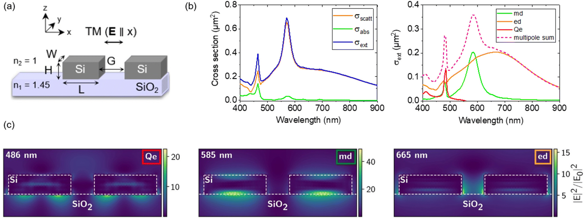 | ||
| Fig. 1 (a) Sketch of the silicon dimer nanoantennas considered for simulations. The dimers are composed of two symmetric rectangular blocks of width W, length L and height H, separated by a gap G. All dimers have a fixed height of H = 90 nm. They lie on a silica substrate and are surrounded by air. (b and c) Examples of simulations for a dimer of dimensions W = 80 nm, L = 280 nm, H = 90 nm and G = 100 nm illuminated by a plane wave polarized along the dimer long axis. (b) Left: extinction (blue), scattering (orange) and absorption (green) cross-sections. Right: multipole decomposition showing the electric quadrupolar (Qe – red), magnetic dipolar mode (md – green) and electric dipolar (ed – orange)mode contribution to the extinction spectrum (pink dashed line). (c) Electric field intensity distribution in and out of the dimer at the resonance wavelengths of λ0 = 486 nm (Qe), 585 nm (md) and 665 nm (ed). | ||
In the case of a dimer with dimensions W = 80 nm, L = 280 nm, H = 90 nm and G = 100 nm, illuminated by a plane wave linearly polarized along the dimer long axis (TM illumination), the cross-section spectra are shown in Fig. 1b. Extinction (blue), scattering (orange) and absorption (green) cross sections are plotted in the left panel of Fig. 1b, showing three resonances around 486, 585 and 665 nm. The negligible absorption cross-section above 500 nm confirms that this silicon dimer can be considered a lossless dielectric nanoantenna.15,50 The multipole decomposition of its extinction spectrum is shown in the right panel of Fig. 1b. The peak around 486 nm corresponds to the electric quadrupolar resonance (Qe) and the peak at 585 nm corresponds to the magnetic dipolar resonance (md), while the broad resonance between 500 and 800 nm is attributed to the electric dipolar mode (ed).51–53 The results in the case of an illumination perpendicular to the dimer long axis (TE illumination), where only a md resonance is excited, can be found in Fig. S1 of the ESI.† The distribution of the electric field intensity inside the dimer (indicated by white dashed lines in Fig. 1c) and in its environment at the resonance wavelengths of 486, 585 and 665 nm is plotted in Fig. 1c. At 585 nm, the electric field intensity maxima are located in the upper and lower sides of the dimer, and in the substrate. This intensity distribution corresponds to a vortex of an electric field, generating a magnetic dipole along the y-axis. In contrast, at 665 nm, the electric field hotspots, though much lower, are interestingly found in the gap of the Si dimer. As the localization of local density of state (LDOS) hotspots (inducing a field enhancement hotspot under illumination) in the gap of dimers has been theoretically predicted and observed many times experimentally, we, therefore, chose to assemble NDs systematically in the gaps of dimers.11,15,17,19,30,45,54
Such simulations were repeated to finally select three dimer geometries: one of non-resonant dimer (W = 80 nm and L = 130 nm), and two of resonant dimers ([W = 80 nm and L = 280 nm] and [W = 130 nm and L = 280 nm]) between λ = 600 and 800 nm, corresponding to the broadband emission spectrum of NV centers. We duplicated each geometry with gaps G of 100, 200 and 300 nm. Such dimers were fabricated by electron-beam lithography (EBL) and anisotropy plasma etching from a SOI substrate. Details about the fabrication of these structures can be found in the Materials & methods section. A complete area containing 90 Si dimers (10 per dimension) is shown in the upper Scanning Electron Microscopy (SEM) image of Fig. 2a. Zoomed SEM images of a few dimers reveal that the nanostructures are well-defined on both sides of the gap. The widths and lengths of the dimers are in accordance with the expected values. Their heights are superior to the 90 nm expected from the Si overlayer thickness of the SOI substrate due to residual HSQ resist on the top of each nanostructure (see the scheme of Fig. 2b). We carefully checked that this residual HSQ layer has a negligible effect on the spectral signature of the dimers.
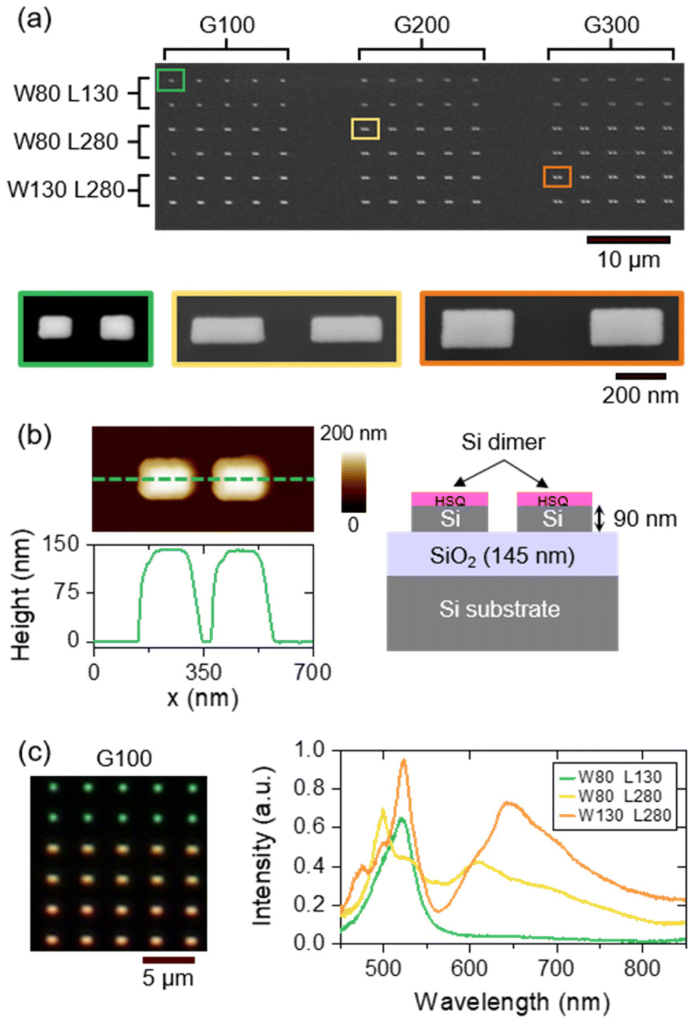 | ||
| Fig. 2 (a) SEM images of silicon dimers fabricated by electron-beam lithography. Each dimer of dimensions W, L and G (all in nanometers) is duplicated 10 times. A complete zone (top) is composed of 90 dimers. Bottom images show SEM zoomed images of 3 dimers. (b) AFM image (top) of the smallest dimer (green-circled in (a)) of dimensions W = 80 nm, L = 130 nm, G = 100 nm, and associated height profile (bottom). (c) Dark-field optical image (left) showing the light scattered by dimers of dimensions [W = 80 nm, L = 130 nm], [W = 80 nm, L = 280 nm] and [W = 130 nm, L = 280 nm] (from top to bottom) with a gap of 100 nm, and the corresponding backward scattering spectra (right). | ||
The optical response of the dimers with the smallest gap G of 100 nm is shown in Fig. 2c. The dark-field optical image of these dimers shows that their color changes depending on their dimensions (width and length increasing from top to bottom) due to different Mie resonances involved.51,55 The experimental backward scattering spectra confirm that the smallest dimers (green-colored) have no resonance between λ = 600 and 800 nm, while the two largest nanoantennas exhibit a broad resonance around 610 nm (W80 L280, yellow-colored) or 650 nm (W130 L280, orange colored), red-shifted and with a higher intensity as the dimensions W and L increase.
Directed assembly of nanodiamonds in the gap of silicon dimers by AFM nanoxerography
AFM nanoxerography consists in the directed assembly of colloidal nanoparticles on electrostatically patterned substrates. It is composed of two main steps: first, charge patterns are written using a polarized AFM tip on a thin film of an electret material. Second, the electrostatically patterned substrate are immersed in a colloidal suspension for a few seconds. Depending on the charge and polarisability of the colloids, the directed assembly of colloidal nanoparticles onto the charge patterns is governed by the electrophoretic and/or dielectrophoretic forces which they induce.33,56In a previous work, we applied this technique to the direct assembly of model negatively charged colloidal quantum emitters (nanodiamonds) on a flat SiO2/Si substrate covered by a PolyMethylMethAcrylate (PMMA) thin film used as an electret. We adapted AFM nanoxerography to successfully assemble a few NDs/NV centers (by maximizing the electrophoretic force to the detriment of the dielectrophoretic force), down to a unique single photon emitter, and with a precision of 50 nm at their position.39
Preliminary study outside the Si dimers
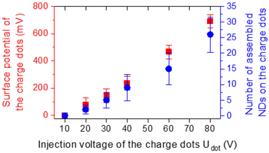
We used the same method and adapted the protocol to couple NDs to crystalline silicon dimers on a patterned SOI substrate. Prior to the assembly of NDs in the gap of those nanoantennas, ND assemblies were fabricated on the bare substrate outside any nanostructure, as a reference. An array of positively charged dots was created by applying voltage pulses with an amplitude Udot from +10 to +80 V to a highly doped silicon AFM tip on the surface of a 90 nm PMMA film deposited on top of the SiO2/Si substrate. The voltage pulses had a width of 1 ms and a frequency of 50 Hz and were applied for 500 ms for each dot. After this charge injection step, the sample was immersed for 30 s in a colloidal suspension of negatively charged NDs purchased from Adamas Nanotechnologies and diluted in ethanol at a concentration C = 2.27 × 10¹² NDs per mL. These colloidal NDs, functionalized by carboxylic groups and initially dispersed in deionised water, have an average diameter of 40 nm as measured by dynamic light scattering and 74% of them nominally contain between 1 and 4 NV centers. During this development step, negatively charged NDs were attracted and trapped on positively charged dots, thanks to electrophoretic forces. The sample was finally immersed in a bath of pure ethanol for 10 s to remove the residual, non-selectively assembled NDs from the substrate. The drying consisted in the natural evaporation of ethanol after taking the sample out of the last bath.Right after charge injection, we measured the maximum surface potential of the dots (averaged on 10 dots) depending on their injection voltage Udot using Kelvin Force Microscopy (KFM). After development, we counted the number of NDs assembled on each charge dot. The evolution of the surface potential of the charge dots (left axis, red squares) and the number of assembled NDs (right axis, blue disks) depending on Udot is plotted in Fig. 3. Both quantities increase with the injection voltage of the charge dots, as reported previously.57–59 As Udot increases, a higher electric field is generated by charge dots, leading to a stronger electrophoretic force exerted over NDs near the surface. Thus, the number of NDs trapped by charge dots is correlated with their surface potential, and increases from 0 to 26 in average in the Udot range considered while the surface potential increases from 0 to 691 mV on average.
 | ||
| Fig. 3 Surface potential of the charge dots (left, red squares) and number of assembled NDs per charge dot (right, blue disks) as a function of the voltage amplitude Udot used for charge dot injection. | ||
Application to the ND diamond assembly in the gap of the silicon dimers
Due to the specifications of the ND suspension used, we determined in previous experiments that assemblies composed of 4 to 6 NDs contain statistically between 0 and 3 NV centers.39 We also noticed that ND assemblies in the gap of silicon dimers are usually composed of fewer NDs than what we observed when the assemblies were fabricated outside of any nanostructure. Considering these two arguments, and in order to target single quantum sources, we chose to fabricate ND assemblies in the gap of our silicon dimers using a fixed dot injection voltage Udot = +40 V, in order to assemble around 5 NDs hosting statistically a single or two NV centers at the end.Fig. 4a shows a schematic representation of a silicon dimer covered by a 90 nm PMMA film (PMMA thickness measured out of any Si nanostructure). The ripples on top of the Si blocks are due to the spin-coating process and substrate wettability.60 The position of the charge dot (at Udot = +40 V) in the gap of the dimer is indicated by a red rectangle. Each charge dot was written in the gap of the 90 dimers as shown in Fig. 2a, by injecting 18 times in a row a charge pattern composed of 5 charge dots spaced horizontally and centered on each dimer on a line. The total injection process lasted 40 minutes. Typical topography and surface potential mappings recorded by AFM/KFM right after charge injection on a line of dimers with a width W = 130 nm, a length L = 280 nm and a gap G = 100 nm are presented in Fig. 4a. The corresponding height profile (left axis, blue) and surface potential profile (right axis, red) are plotted below. We underline that the PMMA surface topography is not affected when using such charge injection conditions. The maxima of surface potential, corresponding to the charge dots, are well aligned in the gap of the dimers and are around 115 mV on average. We would like to emphasize here that the PMMA film exhibits a slight depletion on top of the gap of the dimers. As a consequence, the NDs are expected to be positioned at the same height as the upper surface of the Si blocks, which is a favourable situation for coupling with the structure.19 Typical examples of ND assemblies obtained after development are visible in the AFM topographical images of Fig. 4b, with the gap increasing from left (100 nm) to right (300 nm).
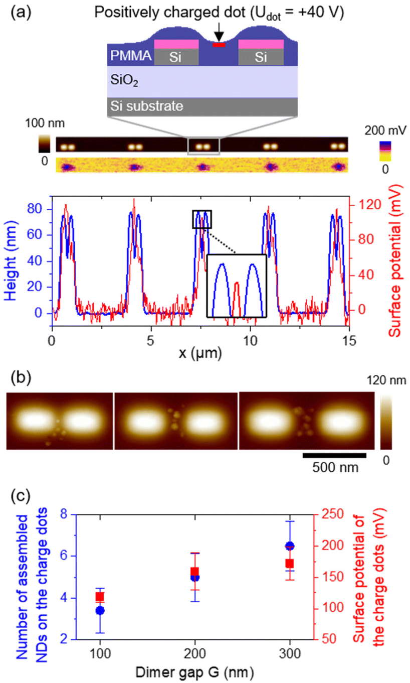 | ||
| Fig. 4 (a) Top: schematic representation of a PMMA film (purple) deposited over a silicon dimer (grey), and a positively charged dot (red) injected in the gap. Middle: AFM topography (top) and KFM surface potential (bottom) maps obtained after injection of a line of positively charged dots in the center of each dimer. Bottom: superimposed height (left, blue) and surface potential (right, red) profiles extracted from the images mentioned above. (b) Typical AFM topographical images of ND assemblies on charge dots in the gap of dimers with W = 130 nm, L = 280 nm and G from 100 to 300 nm (from left to right) after development. (c) Number of NDs trapped in the gaps of dimers after development (left, blue disks) and associated surface potential of charge dots in the gap (right, red squares) measured before development, depending on the dimer gap G. | ||
As expected, a few NDs were selectively trapped in the dimer gap where the positively charged dots were injected. There is an average number of 6 assembled NDs per charge dot in good agreement with the initial target (including all dimensions of dimers), knowing that at least 1 ND has been deposited in the gap of all the 90 dimers. We also notice that the number of assembled NDs per charge dot increases with the dimer gap G. This dependence is plotted in Fig. 4c (left axis, blue disks). This phenomenon is first due to steric hindrance. Indeed, because of the size of the NDs and their negative effective charge (inducing a repulsive Coulomb interaction between NDs), the number of NDs that can be trapped in the gap of a dimer is limited by its dimension. Second, the initial surface potential of charge dots seems to be lower as the gap decreases, due to charge diffusion in the nearby Si blocks. The evolution of the charge dot surface potential with the dimer gap plotted in Fig. 4c (right axis, red squares), decreases actually from almost 172 mV to 118 mV on average when the gap G goes from 300 to 100 nm. Moreover, charge dots were injected into all dimers from top to bottom (towards large W, L) and from left to right (towards large G), so that when the development step was performed, charge dots on dimers with smaller gaps were injected for a longer time (see Fig. 2a). Yet, the charge dissipation over time is responsible for the decrease in the initial amount of injected charges and their surface potential. This phenomenon contributes as well to explain the variations of the number of assembled NDs per charge dot depending on the dimer gap.
Optical characterization of ND assemblies in the gaps of silicon dimers
Typical optical characterization of some ND assemblies is shown in Fig. 5. The PL from each matrix of dimers was acquired using a confocal microscope (see the Material and methods section), a continuous wave (cw) laser at an excitation wavelength λL,cw = 532 nm and with a low power density of 0.0375 MW cm−2. The resulting cartography for a matrix of dimers with a gap G of 100 nm is shown in Fig. 5a. Regular bright dots are visible, allowing us to identify the position of ND assemblies. The brightest spots correspond to dimers with a length of L = 280 nm (and assemblies with a higher number of NDs), while the smallest, corresponding to non-resonant dimers (two first lines), exhibit the same low signal as the residual NDs in the background. Closer PL cartographies have been registered on bright dots (indicating that ND assemblies host at least a single NV center) and their shapes have been compared to AFM topographies of the assemblies. This is the case of the ND assembly/dimer shown in the left panel of Fig. 5b, and corresponds to the dimer labelled as number 1 in Fig. 5a. The localized, intense PL signal comes necessarily from the two NDs trapped in the gap of the dimer because the selectivity is qualitatively excellent around it (only one very small ND is non-selectively deposited out of the charge pattern). Emission spectra were taken systematically for those assemblies and were corrected from the PMMA detrimental contribution (see Fig. S2 in the ESI†). The corrected spectrum given as an example in the right panel of Fig. 5b shows a broadband emission between 600 and 800 nm, providing evidence of the NV center signature. By repeating this procedure, we identified the luminescent assemblies (composed of ND hosting NV centers) with NDs centered in the gap. Then, the second-order correlation function of the emission was measured using a Hanbury Brown & Twiss setup and fitted to determine the number of emitters inside the ND assemblies, given by the relationship g2(0) = 1 − (1/Nspe) at zero delay, with Nspe being the number of single-photon emitters.61 In numerous cases, the second-order correlation function exhibits photon antibunching, with a dip at zero delay (g2(0) < 0.5), indicating the presence of 1 single NV center (or 2 when 0.5 < g2(0) < 0.66), as expected from our previous work.39,61 Several typical ND assemblies are shown in Fig. 5c associating AFM topographies (top) and the corresponding g2(τ) functions (bottom). We note, however, that due to the ND–NV emission statistics and the characteristics of the commercial NDs, the assemblies associated with the photon antibunching host are generally between 1 and 7 NV centers. We therefore successfully demonstrated the possibility to adapt AFM nanoxerography in order to deposit single NV centers in the middle of multiple dimer nanostructures.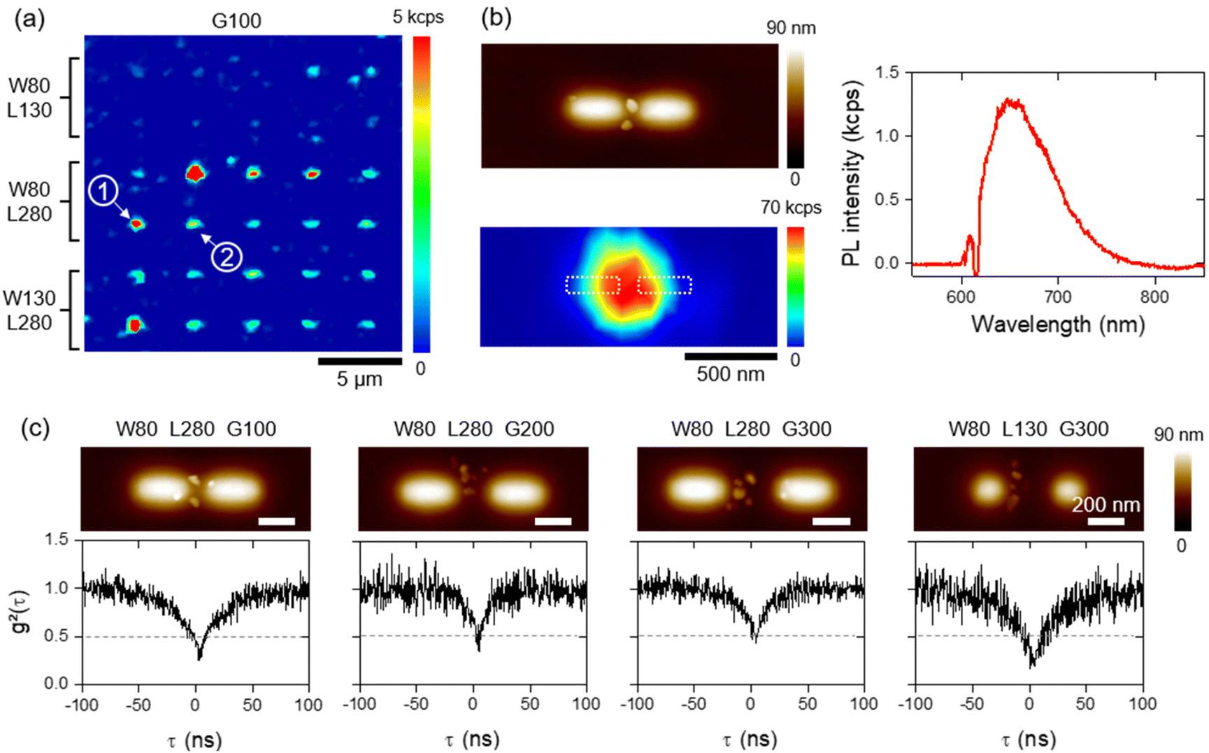 | ||
| Fig. 5 (a) PL color map under a pulsed excitation of 30 assemblies of NDs/dimers with a gap G = 100 nm. (b) AFM topography image of the ND assembly in the gap of the dimer labelled 1 in (a) (top) with the associated PL map under cw excitation (bottom), and typical emission spectrum recorded on an assembly (right, corrected to take into account the PL from PMMA). (c) AFM topography images (top) and associated time-intensity second-order correlation function g2(τ) (bottom) of some ND assemblies containing 1 (g2(0) < 0.5) or 2 (0.5 < g2(0) < 0.66) NV centers. The first left ND assembly of the line corresponds to the dimer labelled 2 in (a). | ||
Incidence of the coupling on the emission of NV centers
The mean PL intensity per ND assembly as a function of the gap G and for the different dimensions L and W of the dimers is plotted in Fig. 6a. One observes that the mean PL intensity decreases as the gap G increases. Its lowest value is reached for the smallest, non-resonant dimers (W80 L130) for which no specific enhancement of the PL was expected from the scattering spectrum, while the PL intensity was drastically higher for longer and larger dimers (up to a 10-fold brightness enhancement with respect to the reference non-resonant dimers). The large error bars associated with these average PL intensity values may partly be due to individual variations in the PL intensity of NDs, including different emitter orientations, which might not be equally collected by the microscope objective. The evolution of the PL intensity may not be attributed to local field enhancement at the excitation wavelength, because the smallest dimer counter-intuitively shows the strongest field enhancement in their gap (see Fig. S3 in the ESI†). Moreover, the PL maps recorded are almost not sensitive to the incident polarization (see Fig. S4 in the ESI†). The fluorescence intensity decay was measured for ND assemblies in the gap of dimers (in green in Fig. 6b) and for dimers covered by PMMA without any NDs (in grey in Fig. 6b). To this end, a pulsed laser at λL,pulsed = 520 nm was used with a repetition rate of 10 MHz.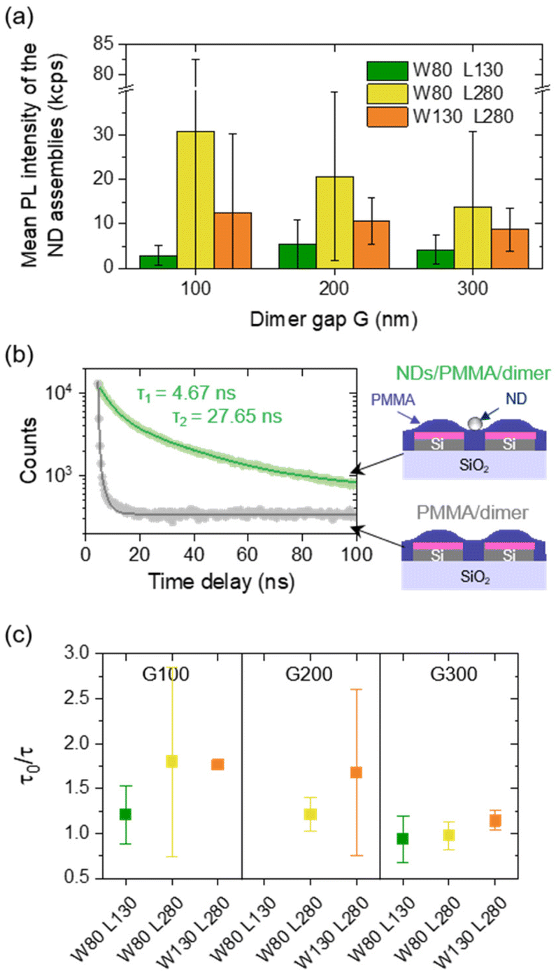 | ||
| Fig. 6 (a) Mean PL intensity of the ND assemblies depending on the gap G, for different widths W and lengths L of dimers. (b) Fluorescence intensity decay measured on an ND assembly in the gap of a dimer covered by a PMMA film (green) and on a dimer covered by PMMA without any ND (grey). Experimental data are fitted by a biexponential decay function. A sketch of both configurations is shown on the right. (c) Mean decay rate enhancement depending on the dimer dimensions and gap, calculated from the ratio between the long-living component of the fluorescence lifetime without (τ0) and with (τ) dimers. | ||
We measured a reference and average long-living component τ0 = 39.7 ± 4 ns on 5 isolated NDs (far from any structure) and reported in Fig. 6c the ratio between this average value and the long-living component τ measured on ND assemblies in the gap of dimers depending on their dimensions. Values of the PL intensity and excited state lifetime were recorded on a subset of 24 ND assemblies with the clearest photon antibunching. Assuming that the non-radiative decay rate is negligible because of low absorption losses in the Si structures, we expect the Purcell factor Fp = τ0/τ to be equal to the normalized radiative decay rate of emitters.4 The graph shows that Fp globally decreases when the gap increases, and for a given gap, the ratio increases with the dimer dimensions (with a maximum Fp = 3.5 measured for intermediate structures W80 L280 G100). These trends are in good agreement with what we observed for the PL intensity. Variations of the normalized decay rate of emitters are therefore directly linked to the PL intensity variations, meaning that the coupling of the NV centers with silicon dimers induces an acceleration of photon emission, therefore leading to an improved, brighter single photon source.
Discussion
Dispersion of the results
As with the PL intensity, large standard deviations are assigned to the average normalized radiative decay rate values. Various factors may explain it. First, because of the specifications of the commercial ND suspension, and stemming from our previous work,39 we chose to assemble a few NDs rather than just one single ND to obtain single-photon-emitter configurations. The position of NDs in the gap slightly changes from case to case, and there is some uncertainty on which ND effectively hosts NV centers. Simulated maps of Fig. 7a illustrate how the normalized decay rate varies depending on the dipole position. The decay rate is averaged under the three perpendicular orientations of an electric dipole emitting at 700 nm (maximum of the NV center emission spectrum), scanned in the xy plane at a height z = 105 nm, slightly above two silicon dimers of dimensions W80 L130 G100 (top) or W80 L130 G300 (bottom), embedded in a PMMA film with a fixed height of 90 nm and lying on a silica substrate. Depending on the position of the electric dipole in the gap G of 300 nm and along the x direction (with y = 0 nm), the normalized decay rate ranges from 1 to ∼2. We also notice from these cartographies that for larger separation of the silicon blocks, we expect the LDOS hotspot to shift from the center of the dimer to its side edges on both sides of the gap, explaining why the experimental normalized decay rate of assemblies (centered on dimers) decreases inversely with the gap (Fig. 6c). The normalized decay rate in the gap also depends on the dipole orientation,62–64 and its height above the dimer/substrate, which is determined by the PMMA thickness at the gap location (see Fig. S5 in the ESI†). We actually observed that the morphology of the PMMA film spin-coated over the nanostructured substrate (and forming a wave as shown in Fig. 4a) and the PMMA thickness in the gap depend on the dimer dimensions and gap (see Fig. S6 in the ESI†). The ND vertical position hence varies according to the ND lateral position in the gap, the dimer dimensions and gap, and the resulting PMMA thickness.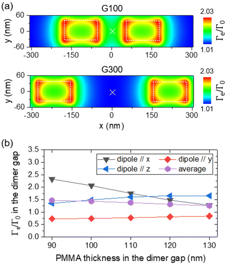 | ||
| Fig. 7 (a) Simulated decay rate maps averaged by the three perpendicular orientations of an electric dipole emitting at 700 nm, scanned in the xy plane 105 nm above a silica substrate, on top of a silicon dimer of width W = 80 nm, length L = 130 nm and height H = 90 nm embedded in a PMMA film of fixed height hPMMA = 90 nm. (b) Simulated normalized decay rate in the exact center of a dimer of width W = 80 nm, length L = 280 nm, and gap G = 100 nm, depending on the PMMA thickness and for different dipole orientations. The dipole–PMMA distance was kept constant at 5 nm. | ||
Fig. 7b illustrates this situation by showing the evolution of the normalized decay rate in the gap of a dimer of dimensions W80 L280 G100 when the PMMA thickness increases (the dipole being systematically scanned 5 nm above it). Depending on the dipole orientation, the normalized decay rate either increases (e.g. from 1.4 to 1.7 for a dipole oriented along z) or decreases (e.g. from 2.3 to 1.3 for a dipole oriented along x) when the PMMA thickens from 90 to 130 nm. Finally, the collection efficiency might also play a role. In emitters positioned on planarized Si dimers19 (configuration rather close to the present system), x-oriented dipoles exhibit a relatively strong contribution in the solid angle given by a 0.9 NA objective. Considering these arguments (dipole position, orientation and height), the experimental values of the normalized decay rate are in fairly good quantitative agreement with the one predicted by our simulations.
Modal analysis
In order to understand the physical mechanism of the coupling and the origin of the Purcell enhancement, we investigated to which mode the dipolar transition is associated with the NV center couples.65 The NV center was modeled as an electric dipole source placed in between the dimer at a height of 90 nm. We used an effective refractive index of 1.33 for the environment accounting for the presence of PMMA and air. Then, we performed simulations of the averaged intensity of the electric field in the Si blocks forming the resonant dimer of intermediate size (W = 80 nm, L = 280 nm, H = 90 nm, and G = 100 nm) as a function of the wavelength. Fig. 8 shows this field intensity average inside the dimer for three electric dipolar orientations: x, y and z. The results reveal that only an x-oriented dipole couples to the structure and gives a non-negligible response in the Si dimer. When compared to the multipole expansion of Fig. 1b (right panel), it turns out that x-oriented dipoles mainly couple with the dimer electric dipole moment along x, which is the main resonant mode in the spectral range of the NV center (600–800 nm). It is consistent with the simulations of Fig. 7b, which predict an enhanced Purcell effect for x-oriented dipoles. This, therefore, confirms that the orientation of the quantum emitters is one of the reasons for the experimental dispersion observed in the decay rates.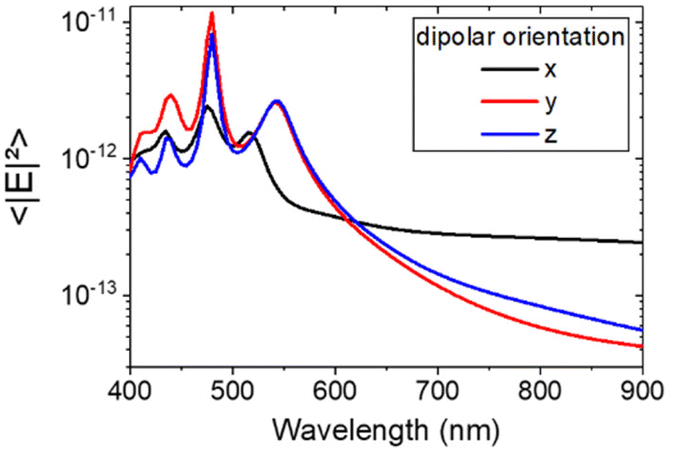 | ||
| Fig. 8 Averaged simulated electric field intensity inside the Si blocks of the dimer plotted in a log scale for the x, y and z-oriented electric dipole source placed in between the dimer at a height of 90 nm. The dimer dimensions are W = 80 nm, L = 280 nm, H = 90 nm, and G = 100 nm. | ||
Conclusions
This work demonstrates, as a proof of principle, that AFM nanoxerography can actually be used to assemble single quantum nanoemitters in the near-field of high-index silicon nanoantennas of simple geometry. Negatively charged NDs, hosting NV centers, selected as a model quantum source, have been electrostatically trapped on charge dots repeatedly and selectively at large-scale on a micrometer-sized surface, in the gaps of several tens of silicon nanodimers, in only a few tens of minutes. Accounting for the specifications of our commercial ND suspension, we deposited on average 6 NDs on purpose in order to maximize the number of ND assemblies hosting a single quantum emitter. The coupling of these single-photon emitters to the silicon dimers leads to an acceleration of photon emission (Purcell factor Fp up to ≈3.5), as a function of the dimensions of the antennas. The modification of the photodynamics originates from a preferential coupling of NV centers oriented along the main axis of the dimers with the dipolar electric Mie resonance building up in the Si blocks. In order to improve the emitter/antenna coupling, the antenna geometry might be optimized, for instance, using an evolutionary algorithm.65,66Finally, thanks to its versatility, AFM nanoxerography could be applied to many colloidal nano-objects, extending this approach to other kinds of single-photon emitters, such as quantum dots, thus paving the way to innovative applications in silicon-based quantum technologies.67
Materials and methods
Dimer fabrication
The patterning of the SOI substrates was performed in a top-down approach by electron-beam lithography (EBL) and subsequent anisotropic plasma etching, in order to define rectangular silicon dimers of different dimensions (the height was defined by the thickness of the SOI silicon layer, which is 90 nm). EBL was carried out on an approximately 60 nm-thick layer of a negative-tone resist (hydrogen silsesquioxane, “HSQ”) with a RAITH 150 writer (electron energy of 30 keV). The resist was developed for 1 min in a solution of 25% tetramethylammonium hydroxide (TMAH). The physical patterning of the silicon overlayer was finally performed by reactive-ion etching (RIE) in an SF6/C4F8 plasma down to the silica substrate, following in situ control.68,69 We noted that a few tens of nm of the developed resist (SiOx with similar optical properties as SiO2) remained on the nanostructures (removal of the residual layer with HF etching resulted in the destruction of the smallest dimers). We did not observe any major impact of this top layer on the optical properties.Confocal microscopy setup
The photoluminescence experiments were performed with a time-resolved confocal luminescence microscope. Either a linearly polarized cw (at λL = 532 nm) or a pulsed (at λL = 520 nm) laser was focused on the sample with a 100× air objective (NA = 0.9). The luminescence was collected using a dichroic mirror centered at λ = 550 nm and a long pass filter centered at λ = 600 nm. The signal was collected using either a single photon avalanche diode (SPAD) for PL mapping and lifetime measurement or two SPADs for intensity correlation acquisitions. The sample was positioned on an xy piezo-scanner.Author contributions
A. C. and L. R. designed the experiments. V. L. and F. F. fabricated and provided the SOI wafer. N. M. and G. L. fabricated the Si nanoantennas. M. H., A. C. and L. R. conducted sample preparation and different nanofabrication steps. M. H., F. G., E. P. and L. R. developed and performed directed assembly by AFM nanoxerography. M. H., V. P. and A. C. implemented the experimental optical setups and performed the optical experiments. M. H., R. H., A. C. and L. R. processed the data. M. H., R. H. and A. C. performed all GDM calculations. M. H., A. C. and L. R. drafted the manuscript, which was amended by all co-authors. All co-authors have given approval to the final version of the manuscript.Conflicts of interest
There are no conflicts to declare.Acknowledgements
The authors thank P. R. Wiecha for fruitful and constructive discussions. This work was supported by the Programme Investissements d'Avenir under the program ANR-11-IDEX-0002-02, reference ANR-10-LABX-0037-NEXT, by the LAAS-CNRS micro and nanotechnologies platform, a member of the French RENATECH network, and by the Agence Nationale de la Recherche (ANR) (Grant No. ANR-19-CE24-0026-HiLight). Calculations were performed using the massively parallel computing center CALMIP in Toulouse (projects P1107, P12167). CEMES and LPCNO acknowledge CNRS and INSA-Toulouse for the Ph. D. grant of M. H. CEMES and LPCNO acknowledge IQO for the postdoctoral fellowship of R. H.References
- J. Wang, F. Sciarrino, A. Laing and M. G. Thompson, Nat. Photonics, 2019, 14, 273–284 CrossRef.
- R. Uppu, F. T. Pedersen, Y. Wang, C. T. Olesen, C. Papon, X. Zhou, L. Midolo, S. Scholz, A. D. Wieck, A. Ludwig and P. Lodahl, Sci. Adv., 2020, 6, eabc8268 CrossRef PubMed.
- N. Li, Y. Lai, S. H. Lam, H. Bai, L. Shao and J. Wang, Adv. Opt. Mater., 2021, 9, 2001081 CrossRef CAS.
- A. F. Koenderink, ACS Photonics, 2017, 4, 710–722 CrossRef CAS PubMed.
- A. E. Krasnok, A. P. Slobozhanyuk, C. R. Simovski, S. A. Tretyakov, A. N. Poddubny, A. E. Miroshnichenko, Y. S. Kivshar and P. A. Belov, Sci. Rep., 2015, 5, 12956 CrossRef CAS PubMed.
- F. Marquier, C. Sauvan and J.-J. Greffet, ACS Photonics, 2017, 4, 2091–2101 CrossRef CAS.
- G. Colas des Francs, J. Barthes, A. Bouhelier, J. C. Weeber, A. Dereux, A. Cuche and C. Girard, J. Opt., 2016, 18(9), 094005 CrossRef.
- A. E. Krasnok, A. E. Miroshnichenko, P. A. Belov and Y. S. Kivshar, Opt. Express, 2012, 20, 6 CrossRef PubMed.
- M. R. Hasan and O. G. Hellesø, Nanotechnology, 2021, 32, 202001 CrossRef CAS PubMed.
- H. Huang, S. Manna, C. Schimpf, M. Reindl, X. Yuan, Y. Zhang, S. F. C. da Silva and A. Rastelli, Adv. Opt. Mater., 2021, 9, 2001490 CrossRef CAS.
- R. Regmi, J. Berthelot, P. M. Winkler, M. Mivelle, J. Proust, F. Bedu, I. Ozerov, T. Begou, J. Lumeau, H. Rigneault, M. F. García-Parajó, S. Bidault, J. Wenger and N. Bonod, Nano Lett., 2016, 16, 5143–5151 CrossRef CAS PubMed.
- M. G. Harats, N. Livneh and R. Rapaport, Opt. Mater. Express, 2017, 7, 834 CrossRef.
- E. Rusak, I. Staude, M. Decker, J. Sautter, A. E. Miroshnichenko, D. A. Powell, D. N. Neshev and Y. S. Kivshar, Appl. Phys. Lett., 2014, 105, 221109 CrossRef.
- P. Kolchin, N. Pholchai, M. H. Mikkelsen, J. Oh, S. Ota, M. S. Islam, X. Yin and X. Zhang, Nano Lett., 2015, 15, 464–468 CrossRef CAS PubMed.
- P. Albella, M. A. Poyli, M. K. Schmidt, S. A. Maier, F. Moreno, J. J. Sáenz and J. Aizpurua, J. Phys. Chem. C, 2013, 117, 13573–13584 CrossRef CAS.
- S. Bidault, M. Mivelle and N. Bonod, J. Appl. Phys., 2019, 126, 094104 CrossRef.
- P. R. Wiecha, C. Majorel, C. Girard, A. Arbouet, B. Masenelli, O. Boisron, A. Lecestre, G. Larrieu, V. Paillard and A. Cuche, Appl. Opt., 2019, 58, 1682 CrossRef CAS PubMed.
- D. Gérard, J. Wenger, A. Devilez, D. Gachet, B. Stout, N. Bonod, E. Popov and H. Rigneault, Opt. Express, 2008, 16, 15297 CrossRef PubMed.
- J.-M. Poumirol, I. Paradisanos, S. Shree, G. Agez, X. Marie, C. Robert, N. Mallet, P. R. Wiecha, G. Larrieu, V. Larrey, F. Fournel, K. Watanabe, T. Taniguchi, A. Cuche, V. Paillard and B. Urbaszek, ACS Photonics, 2020, 7, 3106–3115 CrossRef CAS.
- D. Bouchet, M. Mivelle, J. Proust, B. Gallas, I. Ozerov, M. F. Garcia-Parajo, A. Gulinatti, I. Rech, Y. De Wilde, N. Bonod, V. Krachmalnicoff and S. Bidault, Phys. Rev. Appl., 2016, 6, 064016 CrossRef.
- V. Rutckaia, F. Heyroth, A. Novikov, M. Shaleev, M. Petrov and J. Schilling, Nano Lett., 2017, 17, 6886–6892 CrossRef CAS PubMed.
- M. Peter, A. Hildebrandt, C. Schlickriede, K. Gharib, T. Zentgraf, J. Förstner and S. Linden, Nano Lett., 2017, 17, 4178–4183 CrossRef CAS PubMed.
- Z. Dong, S. Gorelik, R. Paniagua-Dominguez, J. Yik, J. Ho, F. Tjiptoharsono, E. Lassalle, S. D. Rezaei, D. C. J. Neo, P. Bai, A. I. Kuznetsov and J. K. W. Yang, Nano Lett., 2021, 21, 4853–4860 CrossRef CAS PubMed.
- I. Staude, V. V. Khardikov, N. T. Fofang, S. Liu, M. Decker, D. N. Neshev, T. S. Luk, I. Brener and Y. S. Kivshar, ACS Photonics, 2015, 2, 172–177 CrossRef CAS.
- M. Humbert, P. R. Wiecha, G. Colas des Francs, X. Yu, N. Mallet, A. Lecestre, G. Larrieu, V. Larrey, F. Fournel, L. Ressier, C. Girard, V. Paillard and A. Cuche, Phys. Rev. Appl., 2022, 17, 014008 CrossRef CAS.
- T. Veeken, B. Daiber, H. Agrawal, M. Aarts, E. Alarcón-Lladó, E. C. Garnett, B. Ehrler, J. van de Groep and A. Polman, Nanoscale Adv., 2022, 4, 1088–1097 RSC.
- S. Schietinger, M. Barth, T. Aichele and O. Benson, Nano Lett., 2009, 9, 1694–1698 CrossRef CAS PubMed.
- S. Kumar, A. Huck and U. L. Andersen, Nano Lett., 2013, 13, 1221–1225 CrossRef CAS PubMed.
- E. Bermúdez-Ureña, C. Gonzalez-Ballestero, M. Geiselmann, R. Marty, I. P. Radko, T. Holmgaard, Y. Alaverdyan, E. Moreno, F. J. García-Vidal, S. I. Bozhevolnyi and R. Quidant, Nat. Commun., 2015, 6, 7883 CrossRef PubMed.
- M. Geiselmann, R. Marty, J. Renger, F. J. García de Abajo and R. Quidant, Nano Lett., 2014, 14, 1520–1525 CrossRef CAS PubMed.
- M. P. Busson, B. Rolly, B. Stout, N. Bonod and S. Bidault, Nat. Commun., 2012, 3, 962 CrossRef PubMed.
- X. Xing, Z. Man, J. Bian, Y. Yin, W. Zhang and Z. Lu, Nat. Commun., 2020, 11, 6002 CrossRef CAS PubMed.
- E. Palleau, N. M. Sangeetha, G. Viau, J.-D. Marty and L. Ressier, ACS Nano, 2011, 5, 4228–4235 CrossRef CAS PubMed.
- E. Palleau and L. Ressier, Adv. Funct. Mater., 2018, 28, 1801075 CrossRef.
- A. Stemmer, D. Ziegler, L. Seemann, J. Rychen and N. Naujoks, J. Phys.: Conf. Ser., 2008, 142, 012048 CrossRef.
- L. Seemann, A. Stemmer and N. Naujoks, Microelectron. Eng., 2007, 84, 1423–1426 CrossRef CAS.
- P. Moutet, N. M. Sangeetha, L. Ressier, N. Vilar-Vidal, M. Comesaña, S. Ravaine, R. A. L. Vallée, A. M. Gabudean, S. Astilean and C. Farcau, Nanoscale, 2015, 7, 2009–2022 RSC.
- H. Zhang, X. Xing, J. Zhu, T. Chen, Y. Zhang, W. Zhang and Z. Lu, ACS Appl. Mater. Interfaces, 2019, 11, 38347–38352 CrossRef CAS PubMed.
- M. Humbert, Y. Hallez, V. Larrey, F. Fournel, E. Palleau, V. Paillard, A. Cuche and L. Ressier, Nanotechnology, 2022, 33, 215301 CrossRef PubMed.
- I. Aharonovich, S. Castelletto, D. A. Simpson, C.-H. Su, A. D. Greentree and S. Prawer, Rep. Prog. Phys., 2011, 74, 076501 CrossRef.
- P. Balasubramanian, C. Osterkamp, Y. Chen, X. Chen, T. Teraji, E. Wu, B. Naydenov and F. Jelezko, Nano Lett., 2019, 19, 6681–6686 CrossRef CAS PubMed.
- S. K. R. Singam, M. Nesladek and E. Goovaerts, Nanotechnology, 2020, 31, 105501 CrossRef CAS PubMed.
- D. J. McCloskey, N. Dontschuk, D. A. Broadway, A. Nadarajah, A. Stacey, J.-P. Tetienne, L. C. L. Hollenberg, S. Prawer and D. A. Simpson, ACS Appl. Mater. Interfaces, 2020, 12, 13421–13427 CrossRef CAS PubMed.
- U. Kumar, S. Bolisetty, R. Mezzenga, C. Girard, E. Dujardin and A. Cuche, Nanoscale, 2020, 12, 13414–13420 RSC.
- R. M. Bakker, D. Permyakov, Y. F. Yu, D. Markovich, R. Paniagua-Domínguez, L. Gonzaga, A. Samusev, Y. Kivshar, B. Luk'yanchuk and A. I. Kuznetsov, Nano Lett., 2015, 15, 2137–2142 CrossRef CAS PubMed.
- A. Cuche, O. Mollet, A. Drezet and S. Huant, Nano Lett., 2010, 10, 4566–4570 CrossRef CAS PubMed.
- A. Cuche, M. Berthel, U. Kumar, G. Colas des Francs, S. Huant, E. Dujardin, C. Girard and A. Drezet, Phys. Rev. B, 2017, 95, 121402 CrossRef.
- C. Girard, Rep. Prog. Phys., 2005, 68, 1883–1933 CrossRef.
- P. R. Wiecha, Comput. Phys. Commun., 2018, 233, 167–192 CrossRef CAS.
- Z.-J. Yang, R. Jiang, X. Zhuo, Y.-M. Xie, J. Wang and H.-Q. Lin, Phys. Rep., 2017, 701, 1–50 CrossRef CAS.
- P. R. Wiecha, A. Cuche, A. Arbouet, C. Girard, G. Colas des Francs, A. Lecestre, G. Larrieu, F. Fournel, V. Larrey, T. Baron and V. Paillard, ACS Photonics, 2017, 4, 2036–2046 CrossRef CAS.
- J. Yan, P. Liu, Z. Lin, H. Wang, H. Chen, C. Wang and G. Yang, ACS Nano, 2015, 9, 2968–2980 CrossRef CAS PubMed.
- A. E. Miroshnichenko and Y. S. Kivshar, Nano Lett., 2012, 12, 6459–6463 CrossRef CAS PubMed.
- F. Nicoli, T. Zhang, K. Hübner, B. Jin, F. Selbach, G. Acuna, C. Argyropoulos, T. Liedl and M. Pilo-Pais, Small, 2019, 15, 1804418 CrossRef PubMed.
- L. Cao, P. Fan, E. S. Barnard, A. M. Brown and M. L. Brongersma, Nano Lett., 2010, 10, 2649–2654 CrossRef CAS PubMed.
- E. Palleau, N. M. Sangeetha and L. Ressier, Nanotechnology, 2011, 22, 325603 CrossRef CAS PubMed.
- L. Ressier and V. Le Nader, Nanotechnology, 2008, 19, 135301 CrossRef CAS PubMed.
- L. Ressier, E. Palleau, C. Garcia, G. Viau and B. Viallet, IEEE Trans. Nanotechnol., 2009, 8, 487–491 Search PubMed.
- N. M. Sangeetha, P. Moutet, D. Lagarde, G. Sallen, B. Urbaszek, X. Marie, G. Viau and L. Ressier, Nanoscale, 2013, 5, 9587 RSC.
- S. Roy, K. J. Ansari, S. S. K. Jampa, P. Vutukuri and R. Mukherjee, ACS Appl. Mater. Interfaces, 2012, 4, 1887–1896 CrossRef CAS PubMed.
- M. Berthel, O. Mollet, G. Dantelle, T. Gacoin, S. Huant and A. Drezet, Phys. Rev. B: Condens. Matter Mater. Phys., 2015, 91, 035308 CrossRef.
- S. G. Rao, A. Karim, J. Schwartz, N. Antler, T. Schenkel and I. Siddiqi, ACS Appl. Mater. Interfaces, 2014, 6, 12893–12900 CrossRef CAS PubMed.
- A. Issa, I. Izquierdo, M. Merheb, D. Ge, A. Broussier, N. Ghabri, S. Marguet, C. Couteau, R. Bachelot and S. Jradi, ACS Appl. Mater. Interfaces, 2021, 13, 41846–41856 CrossRef CAS PubMed.
- H. J. Shulevitz, T.-Y. Huang, J. Xu, S. J. Neuhaus, R. N. Patel, Y. C. Choi, L. C. Bassett and C. R. Kagan, ACS Nano, 2022, 16, 1847–1856 CrossRef CAS PubMed.
- Y. Brûlé, P. R. Wiecha, A. Cuche, V. Paillard and G. Colas des Francs, Opt. Express, 2022, 30, 20360–20372 CrossRef PubMed.
- P. R. Wiecha, C. Majorel, C. Girard, A. Cuche, V. Paillard, O. L. Muskens and A. Arbouet, Opt. Express, 2019, 27, 29069 CrossRef CAS PubMed.
- I. Aharonovich, D. Englund and M. Toth, Nat. Photonics, 2016, 10, 631–641 CrossRef CAS.
- X.-L. Han, G. Larrieu, P.-F. Fazzini and E. Dubois, Microelectron. Eng., 2011, 88, 2622–2624 CrossRef CAS.
- Y. Guerfi, F. Carcenac and G. Larrieu, Microelectron. Eng., 2013, 110, 173–176 CrossRef CAS.
Footnote |
| † Electronic supplementary information (ESI) available: Simulations of the electric field at the excitation wavelength, simulations of the scattering spectra and LDOS at different heights, details on the PL confocal signal as a function of polarization, details on the parasitic optical contribution of PMMA, and topographical information on the PMMA film. See DOI: https://doi.org/10.1039/d2nr05526k |
| This journal is © The Royal Society of Chemistry 2023 |