
Light emission dynamics of silicon vacancy centers in a polycrystalline diamond thin film
František
Trojánek
 *a,
Karol
Hamráček
a,
Martin
Hanák
a,
Marián
Varga
bc,
Alexander
Kromka
b,
Oleg
Babčenko
b,
Lukáš
Ondič
*b and
Petr
Malý
a
*a,
Karol
Hamráček
a,
Martin
Hanák
a,
Marián
Varga
bc,
Alexander
Kromka
b,
Oleg
Babčenko
b,
Lukáš
Ondič
*b and
Petr
Malý
a
aFaculty of Mathematics and Physics, Charles University, Ke Karlovu 3, 12116 Prague 2, Czech Republic. E-mail: trojanek@karlov.mff.cuni.cz
bInstitute of Physics, Czech Academy of Sciences, Cukrovarnická 10/112, 16200 Prague 6, Czech Republic. E-mail: ondic@fzu.cz
cInstitute of Electrical Engineering, Slovak Academy of Sciences, Dúbravská cesta 9, 84104 Bratislava, Slovakia
First published on 19th January 2023
Abstract
Diamond thin films can be, at a relatively low-cost, prepared with a high-density of light-emitting negatively charged silicon vacancy (SiV) centers, which opens up the possibility of their application in photonics or sensing. The films are composed of diamond grains with both the SiV centers and sp2-carbon phase, the ratio of these two components being dependent on the preparation conditions. The grain surface and the sp2-related defects might act as traps for the carriers excited within the SiV centers, consequently decreasing their internal photoluminescence (PL) quantum efficiency. Here, we show that in a 300 nm thick polycrystalline diamond film on a quartz substrate, the SiV centers in the diamond grains possess similar temperature-dependent (13–300 K) PL decay dynamics as the SiV centers in monocrystalline diamond, which suggests that most of the SiV centers are not directly interconnected with the defects of the diamond thin films, i.e. that the carriers excited within the centers do not leak into the defects of the film. The activation energy ΔE = 54 meV and the attempt frequency α = 2.6 were extracted from the measured data. These values corresponded very well with the published values for SiV centers in monocrystalline diamond. We support this claim by measuring the transient absorption via a pump and probe technique, where we separated the nanosecond recombination dynamics of carriers in SiV centers from the picosecond decay dynamics of polycrystalline diamond defects. Our results show that PL emission properties of SiV centers in polycrystalline diamond thin films prepared via chemical vapor deposition are very similar to those in monocrystalline diamond thereby opening the door for their application in diamond photonics and sensing.
Introduction
In recent years, color centers in diamond have attracted a broad interest due to their unique optical properties and great application potential in quantum communication and information processing, quantum metrology and biosensors.1–3 Besides well-studied nitrogen vacancy centers, negatively charged silicon vacancy (SiV) centers seem to be a very interesting alternative. Most of the photons emitted by an SiV center are concentrated in a zero-phonon line (ZPL), which makes it a promising candidate for being a single photon source.4 The special symmetry of SiV centers leads to a very weak sensitivity to electric fields, a small spectral diffusion and a narrow inhomogeneous distribution of transition frequencies.5 A detailed investigation of the properties of SiV centers is therefore of great importance. The structure of the ground and the first excited electronic states of the SiV center is well known based on both theoretical and experimental works.6,7 Optical measurements have made a significant contribution in this regard. The methods of optical spectroscopy were applied to the SiV ensemble and recently to single SiV centers embedded in monocrystalline diamond. The lifetime of the first excited state of the SiV center as measured usually via photoluminescence (PL) decay was reported to be in the range of 0.5 to 1.6 ns.6,8,9SiV centers are usually created either via ion-implantation into monocrystalline diamond followed by thermal annealing or during the chemical vapor deposition (CVD) growth on a monocrystalline diamond substrate from silane gas.10 In contrast to the expensive growth of monocrystalline diamond, SiV centers can also be prepared in polycrystalline diamond films at a much lower cost and on a larger scale.11,12 However, the structural and sp2-related defects present in polycrystalline diamond add an unwanted background signal to the PL emission and also increase the absorption of the film. These effects can be minimized by optimizing the growth conditions and also via post-processing steps such as thermal annealing or cleaning in acids.13 It is not clear, however, if the defects are also connected with SiV centers via a non-radiative channel. In other words, it is questionable whether polycrystalline diamond defects (grain surface and sp2-related defects) might act as traps for the excited carriers of SiV centers, hence decreasing their internal PL quantum efficiency. The latter is relatively unimportant in a relatively thick (few microns) film where the surface to volume ratio is low;14 however, in thin layers of 100–300 nm, the grain surface and sp2-defects may play an important role in the light emission efficiency of SiV centers. Diamond thin films prepared on a low-index substrate could be considered a promising material for diamond photonic structures provided the coupling of SiV centers to defects can manifest itself as inefficient.
In this paper, we report time-resolved PL and transient absorption measurements of an ensemble of SiV centers in a diamond thin film (300 nm) prepared on a quartz substrate. We observed the nanosecond recombination dynamics of carriers in SiV centers both in time-resolved absorption measurements and in PL measurements under various temperatures, and determined the value of the excited state lifetime. Based on these measurements, we propose a simple scheme of relaxation and recombination processes in our sample. Our results aim to contribute to the knowledge of electron relaxation and recombination processes in SiV centers.
Experimental methods
Sample
A polycrystalline diamond film with embedded SiV centers was prepared by growth in a microwave plasma-assisted chemical vapor deposition (MW CVD) system with a solid Si source placed near a nucleated quartz substrate.15 The fabrication parameters were MW power of 3 kW, CH4/H2 ratio of 1% (3![[thin space (1/6-em)]](https://www.rsc.org/images/entities/char_2009.gif) :300 sccm), pressure of 60 mbar, deposition time of 42 min, and deposition temperature of 750 °C. This led to the diamond film with a thickness of 300 nm and a high density of light-emitting negatively charged SiV centers. The single centers could not be resolved in such a sample and all optical measurements were always performed on the ensemble of SiV centers. The fabrication parameters were optimized to obtain a high sp3/sp2 ratio.
:300 sccm), pressure of 60 mbar, deposition time of 42 min, and deposition temperature of 750 °C. This led to the diamond film with a thickness of 300 nm and a high density of light-emitting negatively charged SiV centers. The single centers could not be resolved in such a sample and all optical measurements were always performed on the ensemble of SiV centers. The fabrication parameters were optimized to obtain a high sp3/sp2 ratio.
Experimental
The Raman spectrum of the prepared diamond film was obtained with a Renishaw inVia Reflex Raman spectrometer equipped with a He–Cd laser with an excitation wavelength of 442 nm.The steady-state PL spectra were measured with a cw laser (excitation wavelength of 532 nm) in order to characterize the quality of SiV centers in our polycrystalline sample. The spectral resolution of this setup was 0.5 nm. The time-resolved PL signal was measured using a Hamamatsu C5680 streak camera coupled to an Acton SP2150 spectrograph. The streak camera was operated in a single sweep regime with a time resolution of 70 ps. PL was excited using an amplified femtosecond laser system (Tsunami & Spitfire, Spectra Physics) followed by a Topas (Light Conversion) tunable optical parametric amplifier with a pulse length of 100 fs and a repetition rate of 1 kHz. The excitation wavelength was 525 nm and the pump fluence on the sample reached about 0.1 mJ cm−2. The laser spot size on the sample was approximately 40 μm. The spectral resolution of this setup was approximately 2 nm. The sample was mounted on a cold finger in a Janis closed-cycle helium cryostat (temperature range of 13–350 K).
The transient transmission was measured using a standard pump and probe technique in which the probe pulse monitored the transmission TE (T0) of the sample after (without) the pump. The results of the pump and probe experiment are presented in the form of normalized differential transmission ΔT/T0 = (TE – T0)/T0. The pump and probe beams were prepared by the splitting of the laser beam produced by a tunable Tsunami femtosecond laser (Spectra Physics) with a repetition rate of 80 MHz and a pulse width of 80 fs. The central wavelength (both pump and probe beams) during the measurement, unless otherwise stated, was 743 nm with a spectral width of 10 nm. The time delay between the pump and probe pulses was varied by an optical delay line. The pump and probe beams were perpendicularly polarized to suppress interference effects and scattered light. The pump fluence reached about 0.4 mJ cm−2, while the probe pulse was about two orders of magnitude weaker. The laser spot diameter was approximately 40 μm. The energy of the transmitted probe pulse was detected by a Si photodiode and measured by a lock-in amplifier. The time resolution of the setup was 150 fs.
Results and discussion
Raman and steady-state PL spectra
Fig. 1a shows the Raman spectrum of the as-prepared film where a distinct D-peak at ≈1332 cm−1 indicates the diamond character of the film. However, the presence of a t-PA peak at ≈1150 cm−1 (trans-polyacetylene chains) and a broad G-band (1450–1650 cm−1 region) attributed to sp2-bonded carbon, which are non-diamond phases usually localized at the diamond grain boundaries, confirms the polycrystalline character of the diamond film.16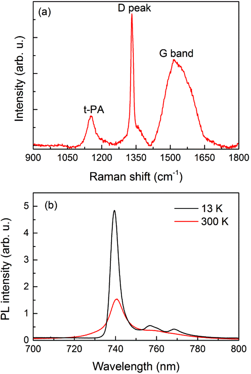 | ||
| Fig. 1 (a) Raman spectrum and (b) cw excited PL spectrum of SiV centers in polycrystalline diamond measured at room and low temperatures. | ||
The steady-state room-temperature and 13 K PL spectra of the SiV center ensembles are shown in Fig. 1b. The zero-phonon PL peak is centered at ≈740 nm at room-temperature but is blue-shifted to ≈739 nm at 13 K. Strong phonon sidebands are clearly resolved at low temperature. At the beginning of the experiment, the PL spectra at room-temperature were measured at various places on the sample and no variation of the SiV peak maximum nor the width was found. The PL spectra correspond well to the previously published spectra of SiV centers. Using a Gaussian fit for the zero-phonon line, we estimated its width to be about 6.5 nm, and the Debye–Waller factor, defined as a ratio of the PL intensity emitted to the zero-phonon line to the whole spectrum, was found to be equal to 0.7. Both values are comparable to those previously reported (both for an ensemble and a single center).5
Temperature dependence of time-resolved photoluminescence
To investigate the dynamics of PL excited by a 100 fs pulse, the excitation wavelength of 525 nm, which is close to the maximum in the PL excitation spectrum of the SiVs,5 was chosen. The time evolution of our sample PL emission spectrum at a low temperature is shown in Fig. 2 where the spectra at 0 ns, 0.5 ns, and 1 ns delays after the excitation pulse are presented. The spectrum has the typical emission features of SiV centers – a strong zero-phonon line emission around 740 nm and a weak phonon sideband, which extends to ≈850 nm. However, as it can be seen in Fig. 2, the SiV emission is superimposed on a spectrally broad and fast band spreading over the whole detection window. We suppose this band originates from various defects in the polycrystalline diamond thin film, such as grain surface defects and/or sp2-related defects.17 The ZPL photoluminescence persists for about 1 ns. In contrast, the defect-related band disappeared very quickly. As an example, the 600 nm-kinetics, the shape of which is limited by the temporal response of the streak camera (70 ps), is shown in the inset of Fig. 2. This confirms the anticipated very fast and effective relaxation of the excited carriers from the higher energy state to the upper level of the PL transition both in the defects and SiV centers.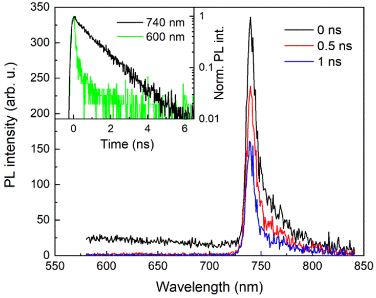 | ||
| Fig. 2 Time evolution of the PL spectrum at a low temperature (12 K). Inset: normalized PL kinetics measured at selected wavelengths (in a semi-log scale). | ||
The ZPL photoluminescence decay (inset of Fig. 2) has a monoexponential character (exp(−t/τ)), which becomes slower with the decreasing temperature. We captured the PL dynamics at various temperatures and extracted the time constant τ by monoexponential fitting. We obtained the temperature dependence of the time constant as shown in Fig. 3. The excited state lifetime was found to increase as the temperature was decreased down to ≈100 K when it flattened at a constant level. This behavior suggests the existence of a non-radiative recombination channel at higher temperatures.
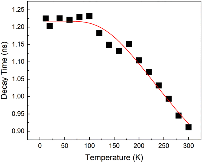 | ||
| Fig. 3 Temperature dependence of the ZPL time constant τ at ≈740 nm. The solid red line is the fit – see text. | ||
Resonant transient absorption
To corroborate the above results of the ZPL decay dynamics, we also performed measurements of the transient optical absorption. While several studies of the PL dynamics of SiV centers in diamonds have been published recently, investigations of the transient absorption are very rare.The room-temperature dynamics of the transient absorption at the resonant wavelength of 743 ± 5 nm is shown in Fig. 4. We can recognize a long component with a nanosecond decay (Fig. 4b) and a very short component with a decay of about one picosecond (Fig. 4a). Around zero-time, where the pump and probe pulses are overlapped, interference effects are visible. Both components have monoexponential decays and therefore we fitted them with single exponential functions obtaining time constants of 1 ps and 0.82 ns.
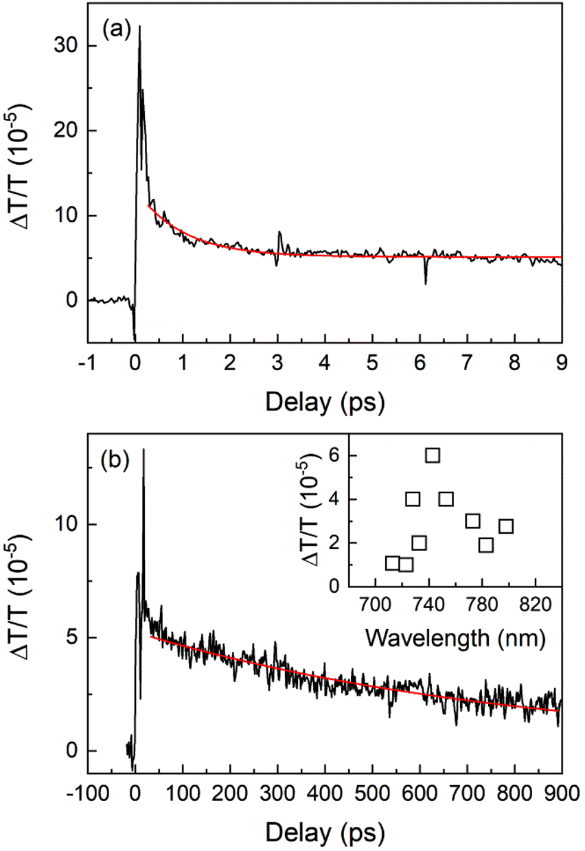 | ||
| Fig. 4 Dynamics of a room-temperature transient transmission at 743 ± 5 nm. (a) Short time-scale measurement; (b) long time-scale measurement. The smooth red curves represent the fits. Inset: the amplitude spectrum of the slow component. | ||
To prove the resonant character of the transient absorption, we performed spectral measurements by tuning the wavelength of both pump and probe beams in the 710–800 nm range. A spectrum of the amplitude of the slow (nanosecond) component is shown in the inset of Fig. 4b. A maximum around the resonance wavelength (743 ± 5 nm) can be clearly recognized. The peak seems to be broadened towards longer wavelengths due to the phonon-assisted absorption. The spectrum of the fast (picosecond) component is very broad (not shown here).
Discussion
Based on our measurements, we propose a simple model of relaxation and recombination processes in the investigated sample. After energetic excitation above the fundamental optical transition of SiV centers, the excited carriers relaxed rapidly (below 1 ps) to the SiV excited state. Then the photons were emitted from SiV centers via ZPL or phonon-assisted PL.The observed ZPL decay time temperature dependence (Fig. 3) can be described by the Mott–Seitz model for non-radiative relaxation, τ = τ0/(1 + αe−ΔE/kBT).6 By fitting the measured data (red solid line in Fig. 3) we obtained the zero decay time τ0 = 1.2 ns, the activation energy ΔE = 54 meV and the attempt frequency α = 2.6. The parameter ΔE can be interpreted using the coordination diagram as the activation energy of phonon-assisted nonradiative recombination. These values corresponded very well with the published values for SiV centers in monocrystalline diamond: ΔE = 55 meV, α = 3.3 and ΔE = 45 meV.6,18
The nanosecond decay time measured using the resonant (≈740 nm) transient absorption (Fig. 4) obviously reflects the lifetime of the excited carriers in the SiV centers. The value is in good agreement, considering the accuracy of our measurement, with PL measurements at 300 K where we observed a decay time of 0.91 ns. Furthermore, the spectrum of the transient transmission amplitude followed the PL spectrum of the ZPL.
On the other hand, we tentatively ascribe the fast 1 ps component at 740 nm either (i) to being a fast nonradiative channel (carrier trapping) in which a portion of the electrons excited in SiV centers are captured or (ii) it possibly being a signature of the grain surface and/or sp2 defects emitting at this wavelength. Taking into account the fact that the amplitude spectrum of this fast component is very broad we assign its origin to the spectrally broad emitting defects of polycrystalline diamond. The value of 1 ps pushes further the resolution-limited value of the defect PL decay dynamics (70 ps) measured with a streak camera. Most importantly, these findings support the results of the temperature-resolved PL dynamics measurements, namely, that the PL of SiV centers in the sample under investigation is not affected by the defects present in polycrystalline diamond.
Our results point towards the conclusion that the majority of light-emitting SiV centers in the prepared sample have comparable optical properties with SiV centers in monocrystalline diamond. It thus shows that SiVs are not connected to defects in polycrystalline diamond and the recombination of excited carriers takes place within the color centers. In comparison with SiV centers prepared via ion implantation into polycrystalline diamond, where the decay dynamics are affected by non-radiative defects,19 our results show that when SiV centers are incorporated during the CVD process from bulk Si, the amount of non-radiative defects in the polycrystalline diamond influencing the PL dynamics of SiV centers is negligible.
Conclusions
We used techniques of time-resolved PL and transient absorption with femtosecond pulse excitation to study the dynamics of photoexcited electrons in SiV centers embedded in a polycrystalline diamond thin film on a quartz substrate. The lifetime of carriers in SiV centers is about 0.9 ns at room temperature and 1.2 ns at low temperatures, respectively. The temperature dependence of the lifetime can be well described by the Mott–Seitz model, which is typical for the presence of a non-radiative recombination channel at higher temperatures. The obtained temperature-dependent decay dynamics and the activation energy have virtually the same values as those for SiV centers in monocrystalline diamond, which indicate that the majority of SiV centers are not linked with defects in the polycrystalline diamond lattice. Moreover, the transient absorption measurement revealed a fast (1 ps) decay component interpreted in terms of carrier recombination through defects in polycrystalline diamond, which is spectrally separated from the SiV centers. Our results show that the PL emission properties of SiV centers in polycrystalline diamond thin films with an optimized sp3/sp2 ratio are very similar to those in monocrystalline diamond, thereby opening the door for their application in diamond photonics or sensing.Author contributions
F. T., K. H., M. H., and P. M. carried out the experiments and analysed the data. M. V., A. K., and O. B. prepared the sample under study and performed the Raman measurements. F. T., P. M., and L. O. conceived the original idea, supervised the project, and wrote the manuscript. All authors reviewed the manuscript.Conflicts of interest
There are no conflicts to declare.Acknowledgements
This work was supported by the grant GACR 19-14523S of the Czech Grant Agency, by the project Lumina Queruntur of the Czech Academy of Sciences, and by the Charles University grant SVV–2022–260590. M. V. acknowledges project no. 19MRP0010 financed from the MoRePro Programme and funding from the Slovak Academy of Sciences. We would like to thank Prof. Ivan Pelant for the fruitful discussion.References
- A. Beveratos, R. Brouri, T. Gacoin, A. Villing, J. P. Poizat and P. Grangier, Phys. Rev. Lett., 2002, 89, 187901 CrossRef PubMed.
- S. Schmitt, et al., Science, 2017, 356, 832 CrossRef CAS PubMed.
- T. D. Merson, S. Castelletto, I. Aharonovich, A. Turbic, T. J. Kilpatrick and A. M. Turnley, Opt. Lett., 2013, 38, 4170 CrossRef CAS PubMed.
- E. Neu, M. Fischer, S. Gsell, M. Schreck and C. Becher, Phys. Rev. B: Condens. Matter Mater. Phys., 2011, 84, 205211 CrossRef.
- S. Häußler, G. Thiering, A. Dietrich, N. Waasem, T. Teraji, J. Isoya, T. Iwasaki, M. Hatano, F. Jelezko, A. Gali and A. Kubanek, New J. Phys., 2017, 19, 063036 CrossRef.
- K. D. Jahnke, A. Sipahigil, J. M. Binder, M. W. Doherty, M. Metsch, L. J. Rogers, N. B. Manson, M. D. Lukin and F. Jelezko, New J. Phys., 2015, 17, 043011 CrossRef.
- L. J. Rogers, K. D. Jahnke, M. W. Doherty, A. Dietrich, L. P. McGuinness, C. Müller, T. Teraji, H. Sumiya, J. Isoya, N. B. Manson and F. Jelezko, Phys. Rev. B: Condens. Matter Mater. Phys., 2014, 89, 235101 CrossRef.
- Y. Rong, J. Ma, L. Chen, Y. Liu, P. Siyushev, B. Wu, H. Pan, F. Jelezko, E. Wu and H. Zeng, Laser Phys., 2018, 28, 055401 CrossRef.
- S. Lagomarsino, A. M. Flatae, H. Kambalathmana, F. Sledz, L. Hunold, N. Soltani, P. Reuschel, S. Sciortino, N. Gelli, M. Massi, C. Czelusniak, L. Giuntini and M. Agio, Front. Phys., 2021, 8, 601362 CrossRef.
- S. Mi, M. Kiss, T. Graziosi and N. Quack, JPhys Photonics, 2020, 2, 042001 CrossRef CAS.
- O. Auciello and D. M. Aslam, J. Mater. Sci., 2021, 56, 7171 CrossRef CAS.
- L. Ondič, M. Varga, J. Fait, K. Hruška, V. Jurka, A. Kromka, J. Maňák, P. Kapusta and J. Nováková, Nanoscale, 2020, 12, 13055 RSC.
- Z. Remes, A. Kromka, M. Vanecek, S. Ghodbane and D. Steinmüller-Nethl, Diamond Relat. Mater., 2009, 18, 726 CrossRef CAS.
- H. Kambalathmana, A. M. Flataea, L. Hunold, F. Sledz, J. Müller, M. Hepp, P. Schmuki, M. S. Killian, S. Lagomarsino, N. Gelli, S. Sciortino, L. Giuntini, E. Wörner, C. Wild, B. Butz and M. Agio, Carbon, 2021, 174, 295 CrossRef CAS.
- S. Stehlik, M. Varga, P. Stenclova, L. Ondic, M. Ledinsky, J. Pangrac, O. Vanek, J. Lipov, A. Kromka and B. Rezek, ACS Appl. Mater. Interfaces, 2017, 9, 38842 CrossRef CAS PubMed.
- M. Varga, T. Izak, V. Vretenar, H. Kozak, J. Holovsky, A. Artemenko, M. Hulman, V. Skakalova, D. S. Lee and A. Kromka, Carbon, 2017, 111, 54 CrossRef CAS.
- P. Galář, B. Dzurňák, M. Varga, M. Marton, A. Kromka and P. Malý, Opt. Mater. Express, 2014, 4, 624 CrossRef.
- B. Dong, C. Shi, Z. Xu, K. Wang, H. Luo, F. Sun, P. Wang, E. Wu, K. Zhang, J. Liu, Y. Song and Y. Fan, Diamond Relat. Mater., 2021, 116, 108389 CrossRef CAS.
- H. Kambalathmana, A. M. Flatae, S. Lagomarsino, H. Galal, F. Tantussi, G. C. Messina, E. Wörner, C. Wild, N. Gelli, S. Sciortino, L. Giuntini, F. De Angelis and M. Agio, Proc. SPIE 11091, Quantum Nanophotonic Materials, Devices, and Systems 2019, 1109108.
| This journal is © The Royal Society of Chemistry 2023 |