
Experimental study on single biomolecule sensing using MoS2–graphene heterostructure nanopores†
Chaoming
Gu
 ab,
Zhoubin
Yu
c,
Xiaojie
Li
ab,
Xin
Zhu
d,
Chuanhong
Jin
c,
Zhen
Cao
ab,
Shurong
Dong
ab,
Jikui
Luo
ab,
Zhi
Ye
*ab and
Yang
Liu
*ab
ab,
Zhoubin
Yu
c,
Xiaojie
Li
ab,
Xin
Zhu
d,
Chuanhong
Jin
c,
Zhen
Cao
ab,
Shurong
Dong
ab,
Jikui
Luo
ab,
Zhi
Ye
*ab and
Yang
Liu
*ab
aCollege of Information Science and Electronic Engineering, Zhejiang University, Hangzhou 310027, P. R. China. E-mail: yezhi@zju.edu.cn; yliu137@gmail.com
bInternational Joint Innovation Centre, Haining 314400, P. R. China
cState Key Laboratory of Silicon Materials, School of Materials Science and Engineering, Zhejiang University, Hangzhou 310027, P. R. China
dChemistry Research Laboratory, Oxford University, Oxford, OX1 3TA, UK
First published on 16th November 2022
Abstract
Solid-state nanopores play an important role in sensing single-biomolecules such as DNA and proteins. However, an ultra-short translocation time hinders nanopores from acquiring more detailed information about biomolecules, and further applications such as sequencing and molecular structure analysis are limited. Related studies have shown that MoS2 has no obvious impediment to biomolecule translocation while graphene may cause obstacles to this process. By combining these two-dimensional materials, nanopores might slow the biomolecule passage. Herein, we fabricated sub-10 nm ultra-thin MoS2–graphene heterostructure nanopores with high stability and tested both dsDNA and native protein (BSA) at the single-molecule level in experiments for the first time. Some special signals with advanced order are observed, which may reflect the shape change of the BSA molecules during the slow translocation process. The results show that the translocation time of BSA is slowed down up to more than 100 ms and the signal length and form are determined by the extent of interaction between the BSA and the heterostructure nanopore. The weak interaction between the BSA and the MoS2 layer increases the translocation probability, and meanwhile, the strong interaction of the graphene layer to BSA slows down the translocation and changes its structure. Therefore, our findings indicate the possibilities of slowing down the single-biomolecule translocation and the capability of acquiring more detailed information about biomolecules using MoS2–graphene heterostructure nanopores.
Introduction
In recent decades, solid-state nanopores have emerged as a new tool with great potential in the detection of single biomolecules such as DNA,1–9 RNA10–12 and proteins.13–15 In order to achieve single biomolecule sequencing and reveal more detailed information from the corresponding ionic blockage signals, the low spatial resolution and the ultra-fast translocation speed are two critical problems that remain to be solved. For spatial resolution, nanopore devices based on two-dimensional materials such as graphene16 and MoS2![[thin space (1/6-em)]](https://www.rsc.org/images/entities/char_2009.gif) 17,18 have been developed, exhibiting the capability of identification of single nucleotides of DNA molecules19 and the detection of proteins with a higher signal-noise ratio.20,21 As to the translocation speed, there are several ways which have been tested to slow down DNA translocation like channel surface charge modulation,22 temperature and bias voltage control,23 edge-field leakage,24 and changing the thin film materials (e.g. hafnium oxide),25 viscosity gradients,19 and pore sizes.26 However, slowing down the protein translocation speed through solid-state nanopores has not yet been investigated systematically, which makes the protein translocation time remain at ∼1 ms.13 Hence few details can be abstracted from single ionic blockage signals.
17,18 have been developed, exhibiting the capability of identification of single nucleotides of DNA molecules19 and the detection of proteins with a higher signal-noise ratio.20,21 As to the translocation speed, there are several ways which have been tested to slow down DNA translocation like channel surface charge modulation,22 temperature and bias voltage control,23 edge-field leakage,24 and changing the thin film materials (e.g. hafnium oxide),25 viscosity gradients,19 and pore sizes.26 However, slowing down the protein translocation speed through solid-state nanopores has not yet been investigated systematically, which makes the protein translocation time remain at ∼1 ms.13 Hence few details can be abstracted from single ionic blockage signals.
Former studies have demonstrated the feasibility of protein detection using graphene21,27,28 or MoS2 nanopores.20,29 For graphene nanopores, there exists a strong surface interaction with protein molecules, leading to hard translocation of the protein molecules through the nanopore.30 Whereas for MoS2 nanopores, this kind of interaction was weaker and in the experiments no obvious barriers were observed for protein translocation.20 Considering this difference between graphene and MoS2, molecular dynamics simulations have been conducted based on the MoS2–graphene heterostructure nanopore31–33 and the results implied that by utilizing the different van der Waals interactions between protein molecules and these two different materials, the protein molecules would move from the MoS2 surface to the graphene surface and be stalled. Therefore, the translocation speed might be slowed down. However, the related works are all about simulations up to now. No experimental studies on heterostructure nanopore fabrication and single-molecule detection have been reported to date to validate the feasibility of this structure for the possible slowing-down effect.
Here, we fabricate MoS2–graphene heterostructure nanopores with various pore sizes using an improved method. The detection experiments of double stranded λDNA and bovine serum albumin (BSA) are conducted and analysed systematically. Compared with MoS2, SiNx and graphene nanopores, the dwell time of BSA translocation is slowed down to more than 100 ms in heterostructure nanopores. The advanced order of some long BSA signals is observed and may reflect the shape change of BSA molecules, which could give us more details about single biomolecules with heterostructure nanopores.
Experimental
Nanopore fabrication
The fabrication process of MoS2–graphene heterostructure nanopores is illustrated in Fig. S1a.† We use a round silicon chip (thickness of silicon: 200 μm, diameter of the chip: 2.8 mm) with a 50 μm × 50 μm silicon nitride (SiNx) free-standing window on the middle of it as the substrate (Norcada Inc.). The thickness of the SiNx thin film is around 15 nm. To make sure that the MoS2–graphene heterostructure is also free-standing on the substrate, a big pore with a diameter of 1 μm is drilled firstly using a focused ion beam (FIB, FEI Quanta 3D FEG with a gallium ion beam) on the centre of the SiNx membrane window as shown in Fig. S1b.† The MoS2 and graphene films are acquired by mechanical exfoliation from the bulk. The exfoliated thin pieces of MoS2 and graphene are picked according to the different colour contrast between the surface of the materials and the background under an optical microscope (Zeiss). Qualitatively, the weaker the contrast of colour is, the thinner the thickness of the material is.34 The definite thickness of the heterostructure is confirmed later by Atomic Force Microscopy (AFM, Bruker Dimension Icon) (Fig. S2†). From AFM analysis we can confirm that the thickness of these structures is in the range of 3 nm–5 nm. The thickness of the graphene membrane is usually slightly thinner than that of MoS2. Later experiments show that this difference in thickness has no obvious effect on biomolecule detection. Subsequently the selected graphene and MoS2 pieces will be transferred and stamped onto the SiNx membrane in sequence by the dry transferring method to cover the pore drilled by the FIB. Using the 3D transferring stage as mentioned in our previous report,20 the materials can be aligned accurately. Fig. S1c and d† show the optical photos of the FIB pore covered by a graphene membrane and then by another MoS2 membrane forming the heterostructure, respectively. During this process, very few extra impurities are introduced and the crystal structure of the materials has fewer defects.35 The electronic diffraction results confirm that both graphene and MoS2 are transferred and are covering the FIB pore, verifying the intactness of the structure (Fig. S3†). The final step is to drill the nanoscale pore on the surface of the MoS2–graphene heterostructure by using a Transmission Electron Microscope (TEM, FEI Tecnai G2 F20). The nanopore diameters can be controlled at 5 nm at the minimum by adjusting the electron dose and the exposure time. In this study nanopores of various sizes have been drilled. Fig. S1e, f and g† show three typical pore diameters under a TEM, which are ∼5 nm, ∼15 nm and ∼20 nm, respectively.Preparation of solutions
In our experiments, four kinds of solutions need to be prepared. Polydimethylsiloxane (PDMS) (Sylgard 184 Silicone) solution is used to seal the nanopore chips. Usually, we use 2 g of PDMS with 0.2 g of curing agent (the weight ratio is 10:1). After thorough mixing the PDMS solution is vacuumed to get rid of the remaining air and set still for about 2–3 hours to decrease its fluidity to some degree, in case the PDMS clogs the nanopore channel. A potassium chloride (KCl) solution is made using 3 g of KCl powder which is dissolved in Tris-EDTA buffer to keep the pH of the KCl solution at 8 so that DNA and BSA molecules will be charged negatively.3,20 The buffer also stabilizes the pH of the solutions during the experiment. The concentration of the KCl solution is adjusted to 1 M and it is filtered to remove other impurities. 1 mg of native BSA powder (Sigma-Aldrich, Merck Ltd) is dissolved and diluted with the prepared KCl solution to 45 nM. λDNA (Sigma-Aldrich, Merck Ltd) is diluted to 0.15 nM using prepared KCl too. Here, the diameter of DNA is ∼2 nm (ref. 36) and the BSA molecule is regarded as an oblate ellipsoid with an ∼14 nm long axis and ∼4 nm short axis.37 The BSA and λDNA solutions are preserved at −18 °C.
Device packaging and wetting
To improve the surface hydrophilicity and nanopore wettability, 3-minute plasma cleaning (Harrick Plasma) is conducted before device packaging. We use the prepared polydimethylsiloxane (PDMS) and two silicone elastomer O-rings (Marian Chicago Inc.) on each side to seal the nanopore chip onto a PCB substrate to make sure that the heterostructure nanopore is the only channel the ionic solution and the biomolecules can flow through. PDMS is solidified at 110 °C on a hot plate. A pair of polytetrafluoroethylene (PTFE) flow cells are used to clamp the chip with two reservoirs, cis and trans. To further wet the nanopore, ethanol is added to cis and trans for about 10–20 minutes and later replaced by a KCl solution.Testing system
The schematic diagram of the testing system is illustrated in Fig. 1a and Fig. S1h.† Two Ag/AgCl electrodes, connected with a patch clamp amplifier (Axon 200B), are immersed in a KCl solution of two reservoirs separately. A patch clamp is used to apply and change the bias voltage across the nanopore as well as inspect the instantaneous ionic current value. An A/D converter (Axon 1550) is connected to the patch clamp and the computer so that the ionic current can be recorded in digital format. We apply the bias voltage through the patch clamp ranging from −600 mV to 600 mV based on different pore sizes. For small pores (diameter ≤ 10 nm), the range is usually from ±400 mV to ±600 mV. For big pores (diameter > 10 nm), the range is usually from ±100 mV to ±400 mV. This difference is related to the threshold voltage of various pore sizes. In this system, the biomolecules will translocate from MoS2 to graphene driven by the bias voltage. The sampling frequency of the patch clamp is 100 kHz. | ||
| Fig. 1 (a) The schematic of the testing system. (b) A transmission electron microscopy picture of a MoS2–graphene heterostructure nanopore with a diameter of ∼5 nm (Scale bar: 5 nm). (c) Open pore I–V curves of heterostructure nanopores with diameters of ∼5 nm, ∼15 nm and ∼20 nm and theoretical conductance values. (d) Power spectrum density vs. frequency curves in nanopores with different pore sizes at 400 mV bias. (e) Three BSA translocation traces at 400 mV bias in nanopores with diameters of ∼5 nm, ∼15 nm and ∼20 nm from top to bottom. | ||
Results and discussion
Electrical characterization of devices
To verify the fundamental function of MoS2–graphene heterostructure nanopores, basic electrical characterization is conducted prior to the biomolecule translocation test. Fig. 1c shows the open pore I–V relationships of three heterostructure nanopores with different diameters, namely, ∼5 nm, ∼15 nm and ∼20 nm at the bias voltage from −400 mV to 400 mV. These data are also compared with a theoretical current value calculated from the equation of nanopore conductance:38,39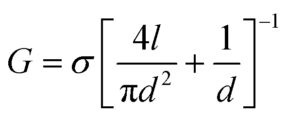 | (1) |
In this equation, σ represents the electrolyte conductivity of the solution, d is the diameter of the nanopore, and l is the length of the nanopore channel. In our work, σ = 10.5 S m−1,40l = 3 nm, and the specific value of d is based on the actual diameter of the nanopores. We can see from Fig. 1c that the experimental data points fit the theoretical lines well and the I–V curves are symmetrical, indicating the good working state of these devices. The I–V curves are basically linear, which means the resistance caused by surface charges in the nanopore channel can be ignored.38
Low-frequency noise or 1/f noise is evaluated for all the devices by power spectrum density analysis. Fig. 1d, Fig. S4 and S5† show the dependency of low-frequency noise on the pore sizes and the bias voltages. The 1/f noise is inversely proportional to the pore size at the same bias voltage and increases when the bias becomes higher in the same pore. These relations are consistent with the related reported study.41 Since the thickness of the heterostructure is much thinner compared with the nanopore diameter in big pores, the pore resistance is dominated by the access resistance. Therefore the 1/f noise does not exactly follow the traditional Hooge's relation. Besides, the mechanical fluctuation of the membrane, as an important factor contributing to the 1/f noise, has less influence on the ionic current in big pores than in small pores. Thus, the 1/f noise changes inversely with the pore size in our devices. The noise level shown in Fig. 1d is in a reasonable range, and the biomolecule translocating traces in the later experiments (Fig. 1e) show that this noise level has no significant influence on single biomolecule detection. According to our previous work, thicker PDMS sealing may decrease the noise to some degree.20
Basic translocation and frequency
For the translocation experiments, nine samples of working heterostructure nanopore devices are tested, of which 6 devices are tested for BSA translocation and 3 devices are tested for λDNA translocation. Following the experimental setup illustrated in Fig. 1a, we record the translocation signals of λDNA and BSA protein. Fig. 1e shows three BSA translocation traces for various pore sizes. From top to bottom the traces are recorded in nanopores with diameters of 5 nm, 15 nm, and 20 nm at 400 mV. A 20 kHz low pass filter is applied in the meantime. Three DNA translocation trace examples with other pore diameters are also shown in Fig. S6.† Different pore sizes have some influences on the threshold voltage and translocation rate. The nanopores with pore sizes larger than 15 nm usually begin to have translocation signals at 100 mV–200 mV, while signals can only be found in nanopores with a diameter of ∼5 nm at 400 mV or above. It probably indicates that a bigger pore lowers the entrance barrier and facilitates the biomolecules to translocate through the nanopore. This result is similar to our previous work on MoS2 nanopores.42 At 400 mV bias voltage, the average translocation rates of BSA in nanopores with diameters of 5 nm, 15 nm and 20 nm are ∼0.1, ∼0.15 and ∼0.34 events per second, respectively. And those of λDNA in nanopores with diameters of 7 nm, 10 nm and 14 nm are ∼0.22, ∼0.3 and ∼0.5 events per second, respectively. Bigger pore sizes improve the translocation rate, which is consistent with the Smoluchowski rate equation.43 The translocation rate of DNA is nearly 2 times higher than that of BSA. The protein adsorption onto the surface of the materials might explain this phenomenon.44 With the bias voltage increasing, the translocation rates of both BSA and DNA are found to become higher for the same pore size.15,45Statistical analysis of BSA translocation
Biomolecule translocation signals are identified and analysed using Transalyzer software.46 Table S1† lists the translocation details of all six devices for BSA translocation. Fig. 2a and b show the scattered plots of the BSA signals’ amplitude vs. dwell time in two heterostructure nanopores with diameters of ∼5 nm and ∼15 nm, respectively (devices 2 and 4). The density distributions of the dwell time and blockage current are plotted in the margins as well. All the devices are tested for nearly 2 hours and the signals are continuously captured. After 2 hours, few signals can be detected due to the adsorption onto the graphene surface reaching saturation.31 The bias range is from 400 mV to 600 mV for device 2 and from 200 mV to 400 mV for device 4. For both devices, as the bias voltage increases, the peak of the ΔI distribution moves to a higher value (Fig. 2a and b).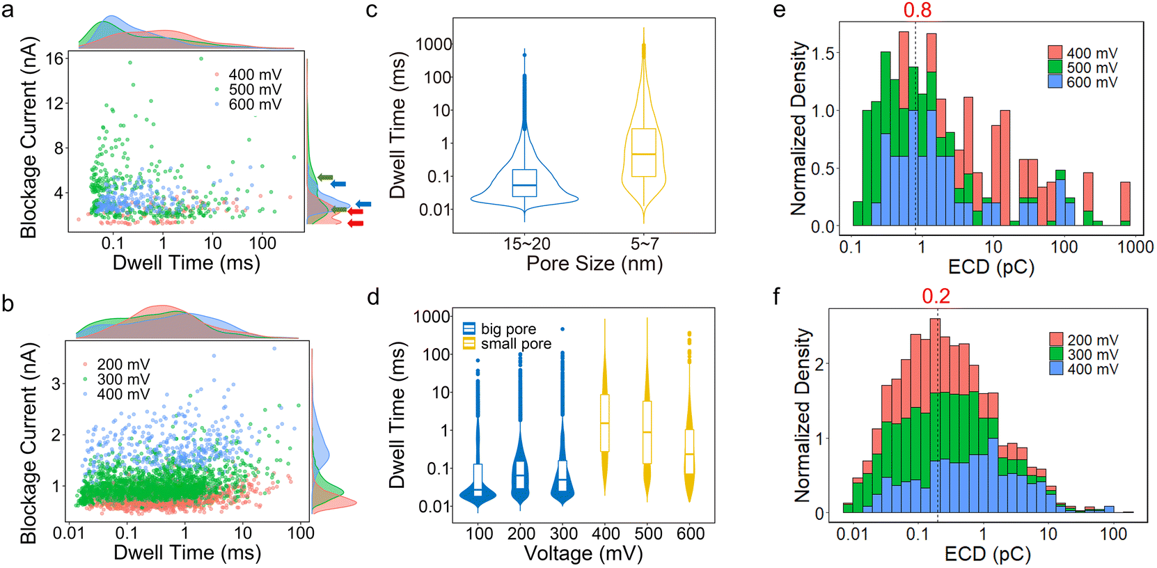 | ||
| Fig. 2 (a) and (b) Scatter plots of blockage current vs. dwell time of device 2 (5.09 nm) and device 4 (15.62 nm) with the corresponding density distribution on margins at different bias voltages. (c) Violin and boxplots of dwell time distribution vs. pore size of all six devices. The blue one represents the pore size from 15 nm to 20 nm and the yellow one represents the pore size from 5 nm to 7 nm. (d) Violin and boxplots of dwell time vs. bias voltage of all six devices. The range of pore sizes is the same as that in (c). Electrical charge deficit histogram distributions of (e) device 2 and (f) device 4. Dashed lines mark the ECD peak. | ||
In small pores, the distribution of blockage current seems to appear in two clusters as shown in Fig. 2a and Fig. S7.† In Fig. 2a, the lower clusters correspond to 0.4 nA, 2.5 nA and 3 nA, and the higher clusters correspond to 2.4 nA, 5.5 nA and 5 nA at 400 mV, 500 mV and 600 mV, respectively. The lower cluster probably means that the BSA molecules do not fully translocate through the nanopores.13 Using a protein excluded volume model,14 we estimate that the maximum value of a signal in small pores should be above ∼2.3 nA. Therefore, the lower cluster at 400 mV and signals at 500 mV and 600 mV with blockage current smaller than 2.3 nA are dismissed and not included in the latter analysis. In Fig. S7,† all lower clusters are smaller than 2.3 nA, and therefore these signals should all be omitted. In big pores (diameter > 10 nm), no second cluster appears in the signal distribution of blockage current and all signals match the model estimation mentioned above.
The dwell time distribution is analysed in the margin of Fig. 2a and b and more specifically, in Fig. S8.† Most of the signals have a short dwell time, concentrated in 0.01–1 ms, indicating that the BSA translocation speed is still fast. The same situations are also found in SiNx and MoS2 nanopores. However, a non-negligible portion of signals shows a dwell time longer than 10 ms and even 100 ms in small pores. Statistically, signals longer than 10 ms in small pores (devices 1, 2, 3) are larger than 10%, and signals longer than 100 ms are about 8.1%, 1.4% and 0.6% for the three devices, respectively. In big pores (devices 4, 5, 6), however, the proportion of long signals is smaller compared to the small pores, and only a few signals are longer than 100 ms, as shown in Table S1.†Fig. 2c shows the dwell time distribution of all six devices based on different pore sizes. It clearly shows that there is a larger portion of signals longer than 10 ms in small pores than in big pores.
We also investigate the relationship between the bias voltage and the dwell time in Fig. 2d. For big nanopores, the change in bias voltage has no considerable influence on the dwell time distribution at 200 mV and 300 mV. While at 100 mV, the number of signals is small and most of them have shorter dwell times. For small pores, as the bias voltage increases, shorter signals become more in number and the number of signals longer than 10 ms decreases from 23% to 5%, but its proportion is still higher than the big pores.
To further verify that the heterostructure nanopores indeed can prolong the BSA translocation dwell time, they are compared with three other types of nanopores, namely MoS2, graphene and SiNx nanopores. Fig. 3a shows the comparison of the dwell time distribution between the heterostructure and MoS2 nanopores with a diameter of ∼7 nm and thickness of ∼3 nm at 500 mV. Of all effective signals, nearly no signal longer than 10 ms is observed in MoS2 nanopores. And the distribution in the range of 1–10 ms is lower than the heterostructure nanopore as well. Four traditional ∼15 nm thick SiNx nanopores with diameters ranging from 9 nm to 25 nm are tested for BSA translocation as well. Fig. 3b shows the BSA translocation dwell time comparison between the heterostructure nanopore and the SiNx nanopore with a diameter of 7 nm at 500 mV. It is clearly shown that in the range of 1–100 ms the distribution of the heterostructure nanopore is much higher than that of the SiNx nanopore. And for the SiNx nanopore, there are no signals longer than 100 ms. The detailed results of SiNx nanopores with various pore sizes are also listed in Table S2,† showing again that no signals longer than 100 ms are detected, and the ones longer than 10 ms are all lower than those of 1% of all the devices quantitatively. Hence, from Fig. 3a and b we notice that even though the distribution peaks of dwell time among these three different nanopores are all close to 0.1 ms, the tail of distribution for the heterostructure nanopore is much longer and more distinct than the other two. Four graphene nanopore samples are also fabricated but cannot detect any BSA translocation signals without further surface modifications (Fig. 3c) due to the strong interaction between BSA and the graphene surface.21,27 The corresponding BSA translocation traces of these four types of nanopores are shown in Fig. 3c and we can see that the heterostructure nanopore (red) has a relatively higher signal-noise-ratio (SNR) than the MoS2 nanopore due to its ultra-thin thickness compared to the SiNx nanopore. Besides, the PSD analysis (Fig. 3d and Fig. S9†) indicates that the noise level of the heterostructure nanopores is even lower than that of MoS2 nanopores at the same voltage. Therefore, the heterostructure nanopores slow down BSA translocation, and in the meantime preserve the high SNR and relatively low noise, demonstrating better overall performance than SiNx, MoS2 and graphene nanopores.
 | ||
| Fig. 3 (a) The BSA translocation dwell time comparison between the heterostructure nanopore (M–G) and the MoS2 nanopore. (b) The BSA translocation dwell time comparison between the heterostructure nanopore (M–G) and the SiNx nanopore. Both (a) and (b) are compared at 500 mV bias voltage, and the diameters of the nanopores are all around 7–9 nm. (c) Four translocation traces of SiNx, MoS2, graphene and heterostructure nanopores (from top to bottom) at 400 mV. The pore sizes of the four nanopores are ∼7 nm. (d) Power spectrum density vs. frequency curves of four types of nanopores, including SiNx, MoS2, graphene and heterostructure nanopores. | ||
In general, the nanopore length (the membrane thickness) and the bias voltage can influence the translocation speed, i.e., the dwell time. When the nanopore length and the bias voltage are longer and lower respectively, the translocation of molecules through the nanopore tends to be slower.15,47 According to our experiments, however, the slowing-down effect of BSA molecules is hardly observed in similar (MoS2 nanopores) or even longer nanopore lengths (SiNx nanopores). It is found from Fig. 2d that for the heterostructure nanopores, different bias voltages affect the translocation dwell time to a very small extent. The pore size plays a relatively important role in the dwell time. For smaller nanopores, the chance that BSA molecules interact with the pores becomes higher, and this interaction may slow the translocation due to the different van der Waals interaction between the molecules and two different materials, of which graphene has a stronger interaction with the molecule and may stall the translocation process.31 From the experimental data we do find longer BSA signals for the heterostructure devices with smaller pore sizes. Conversely, even though the pore size is small (<10 nm), the long signals are still rare in MoS2 and SiNx nanopores (Fig. 3a and b), indicating that a small pore size has less influence on the BSA translocation dwell time in MoS2 and SiNx nanopores due to the weak BSA–nanopore interaction. These results probably indicate that the MoS2–graphene heterostructure has the effect of slowing down the BSA translocation.
ECD (electric charge deficit) analysis is conducted and shown in Fig. 2e and f to further confirm this interaction.3 For big pores (Fig. 2f), the ECD distribution is concentrated at ∼0.2 pC, around 10 times larger than the traditional SiNx nanopores (∼0.016 pC).13 For small pores (Fig. 2e), the peak of ECD is about 0.8 pC, ∼50 times larger than that of the SiNx nanopores, and more than 2 times larger than that of the MoS2 nanopores (∼0.3 pC). Therefore, in heterostructure pores, the interaction between BSA and the MoS2–graphene structure plays an important role in BSA translocation, which may influence the different types of signals and their dwell times.4
Single signal analysis of BSA
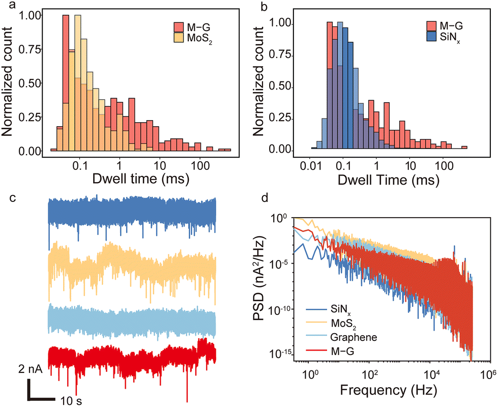
To further investigate the slowing-down effect of BSA translocation, individual signals are inspected closely. According to the translocation dwell time, there are three types of signals in heterostructure nanopores. Fig. 4a shows that the first type are shorter signals (<1 ms), occupying 57.3% and 94.5% in small and big pores, respectively. Most of them exhibit the shape of a pulse and no flat stage. The second type are signals with a stage part and their dwell times are in the range of 1–100 ms (Fig. 4b, c and d), which account for 37.2% and 5.4% in small and big pores, respectively. The third type are the signals longer than 100 ms as shown in Fig. 4e. The percentage of this type to the total is 5.5% in small pores and less than 0.1% in big pores. The latter two types have a relatively higher ratio in small pores than in big ones, which may indicate that in small pores the effect of the BSA–heterostructure interaction is stronger than that in big pores. Among these types of signals, only the first type can be found in MoS2 and SiNx nanopores, and the second type appears much rarely (only a few signals with dwell times from 1 ms to 10 ms). | ||
| Fig. 4 Various BSA translocation signals: (a) a typical type-1 signal, (b) and (c) two special type-2 signals, (d) a typical type-2 signal and (e) a typical type-3 signal. Below them are their corresponding translocation schematics. The arrows signify the translocation direction of BSA. | ||
The dwell times and their signal forms are possibly determined by the extent of the interaction strength. For the signals of the first type, as shown in Fig. 4a, the interaction is weak and BSA molecules translocate through the nanopore fast. For the second type, the interaction is relatively stronger and there exists direct contact between BSA and the heterostructure, especially with the graphene layer. Here two special kinds of second type signals in small pores with a second order stage are shown in Fig. 4b and c. The second stage mostly appears at the beginning, like Fig. 4c, and a few have this second stage in the middle (Fig. 4b). These phenomena are similar to DNA signals, but the original mechanism is different since the native protein molecules cannot be folded or knotted. We have found these types of signals in MoS2 nanopores with a diameter of ∼20 nm caused by concurrent translocation of two or more BSA molecules or by a change in orientation during the translocation.42,48 However, considering the geometry of BSA molecules (14 nm × 4 nm oblate ellipsoid),37 and the small pores with a diameter of ∼5 nm, it is unlikely that two or more molecules translocate concurrently or in a single file to cause this second order in heterostructure nanopores.49 In both big and small pores, the distribution of effective blockage current has only one peak at the lower part of the ΔI, and using the equation
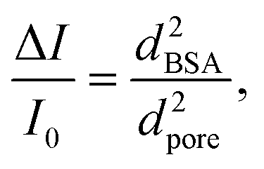 | (2) |
Statistical analysis of λDNA translocation
A λDNA translocation test is conducted in 3 heterostructure nanopore devices, and their signal distribution is shown in Fig. 5. For devices with nanopore diameters of 10 nm and 14 nm (seen in Fig. 5e and h), two peaks of blockage current can be identified. According to the previous work,5 these two peaks represent different kinds of DNA configuration, e.g. linear, folded or circular configurations. While in a nanopore with a diameter of 7 nm (Fig. 5b), the higher-step peak is not clear and most of the DNA molecules are translocated linearly. This is probably because the DNA molecules with complex configurations are not easy to translocate through the small nanopore. The histograms of the dwell times of the three devices are also shown in Fig. 5c, f and i. Compared to the SiNx nanopores with a diameter of ∼15 nm (Fig. S10†), the distribution mode and the portion of the long signals (>10 ms) in heterostructure nanopores are similar to those in SiNx nanopores. The related simulation results indicate that the geometry of the nanopores influences the DNA translocation speed,56 and the circular pore as we fabricated has a weaker interaction with DNA than rectangular and triangular ones. Thus, there is no obvious effect of slowing down the λDNA translocation in our heterostructure devices due to the relatively weak interaction between DNA and the heterostructure.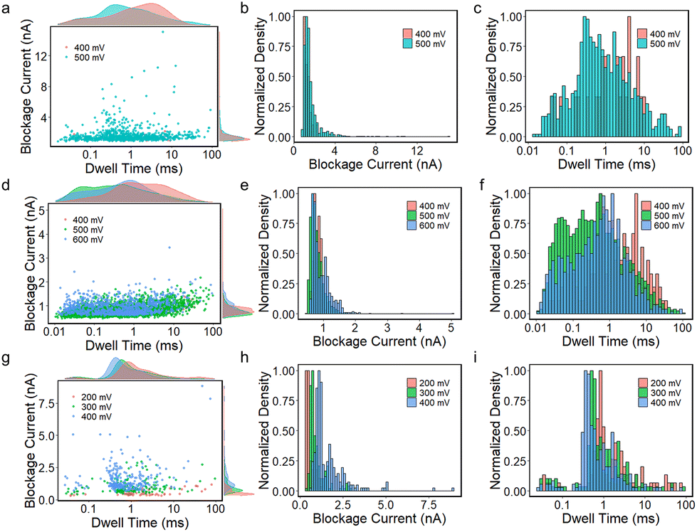 | ||
| Fig. 5 (a), (d) and (g) The scatter plots of dwell time vs. blockage current of DNA translocation signals from three heterostructure nanopores with various pore sizes. (b), (e) and (h) The normalized histogram distribution of blockage current of DNA translocation. (c), (f) and (i) The normalized histogram distribution of the dwell time of DNA translocation. From top to bottom: the diameters of three nanopores are ∼7 nm, ∼10 nm and ∼14 nm, respectively. | ||
Conclusions
In conclusion, the MoS2–graphene heterostructure nanopores with various pore sizes are fabricated. The λDNA and BSA molecules are tested for translocation, and signals are inspected in different pore sizes and bias voltages. Compared to MoS2 and SiNx nanopores, the presented structure can prolong the dwell time of BSA translocation up to several hundred milliseconds owing to the interaction between BSA molecules and the heterostructure. While there isn't any obvious similar effect for DNA. Further investigation of single BSA signals shows that slow translocation and interaction may affect the shape of BSA molecules, leading to the acquisition of more information. Our experimental results imply that the heterostructure nanopores have potential in slowing down protein translocation and acquiring more information about single biomolecules. For future research, more kinds of proteins could be tested, and the deeper physical mechanism can be studied by molecular dynamics simulations, enhancing our understanding of this type of nanopore.Author contributions
Chaoming Gu: conceptualization, methodology, validation, formal analysis, investigation, data curation, writing – original draft, visualization, and project administration. Zhoubin Yu: conceptualization, methodology, investigation, and resources. Xiaojie Li: validation and investigation. Xin Zhu: validation, formal analysis, and writing – review & editing. Chuanhong Jin: resources and supervision. Zhen Cao: resources and supervision. Shurong Dong: resources and supervision. Jikui Luo: resources and supervision. Zhi Ye: conceptualization, validation, formal analysis, resources, writing – review & editing, supervision, project administration, and funding acquisition. Yang Liu: resources, writing – review & editing, supervision, project administration, and funding acquisition.Conflicts of interest
The authors declare no competing financial interests.Acknowledgements
This work was supported in part by the NSFC under Grant 61774132, 61501401 and 61574126, the National Science Foundation of Zhejiang Province, China, under Grant LZ20F040003 and LY16F010006, and the Sichuan Science and Technology Agency, under Grant 2019YFSY0043.References
- K. Briggs, G. Madejski, M. Magill, K. Kastritis, H. W. de Haan, J. L. McGrath and V. Tabard-Cossa, Nano Lett., 2018, 18, 660–668 CrossRef CAS.
- C. Dekker, Nat. Nanotechnol., 2007, 2, 209–215 CrossRef CAS.
- D. Fologea, M. Gershow, B. Ledden, D. S. McNabb, J. A. Golovchenko and J. Li, Nano Lett., 2005, 5, 1905–1909 CrossRef CAS.
- R. Kumar Sharma, I. Agrawal, L. Dai, P. S. Doyle and S. Garaj, Nat. Commun., 2019, 10, 4473 CrossRef.
- C. Plesa, D. Verschueren, S. Pud, J. van der Torre, J. W. Ruitenberg, M. J. Witteveen, M. P. Jonsson, A. Y. Grosberg, Y. Rabin and C. Dekker, Nat. Nanotechnol., 2016, 11, 1093–1097 CrossRef CAS PubMed.
- X. Zhu, X. Li, C. Gu, Z. Ye, Z. Cao, X. Zhang, C. Jin and Y. Liu, ACS Nano, 2021, 15, 9882–9889 CrossRef PubMed.
- J. Zhu, F. Bošković and U. F. Keyser, Nano Lett., 2022, 22, 4993–4998 CrossRef CAS PubMed.
- X.-L. Xing, Q.-B. Liao, S. A. Ahmed, D. Wang, S. Ren, X. Qin, X.-L. Ding, K. Xi, L.-N. Ji, K. Wang and X.-H. Xia, Nano Lett., 2022, 22, 1358–1365 CrossRef CAS.
- R. Hu, C. Liu, W. Lu, G. Wei, D. Yu, W. Li, P. Chen, G. Li and Q. Zhao, Nano Lett., 2022, 22, 888–895 CrossRef CAS.
- M. van den Hout, I. D. Vilfan, S. Hage and N. H. Dekker, Nano Lett., 2010, 10, 701–707 CrossRef CAS.
- M. Wanunu, S. Bhattacharya, Y. Xie, Y. Tor, A. Aksimentiev and M. Drndic, ACS Nano, 2011, 5, 9345–9353 CrossRef CAS PubMed.
- H. Kaur, S. Nandivada, M. C. Acharjee, D. S. McNabb and J. Li, ACS Sens., 2019, 4, 100–109 CrossRef CAS PubMed.
- D. Fologea, B. Ledden, D. S. McNabb and J. Li, Appl. Phys. Lett., 2007, 91, 053901 CrossRef PubMed.
- J. Li, D. Fologea, R. Rollings and B. Ledden, Protein Pept. Lett., 2014, 21, 256–265 CrossRef CAS.
- B. Cressiot, A. Oukhaled, G. Patriarche, M. Pastoriza-Gallego, J.-M. Betton, L. Auvray, M. Muthukumar, L. Bacri and J. Pelta, ACS Nano, 2012, 6, 6236–6243 CrossRef CAS.
- S. Garaj, S. Liu, J. A. Golovchenko and D. Branton, Proc. Natl. Acad. Sci. U. S. A., 2013, 110, 12192–12196 CrossRef CAS.
- D. J. Niedzwiecki, B. DiPaolo, C.-Y. Lin, A. Castan, R. Keneipp and M. Drndić, ACS Sens., 2021, 6, 2534–2545 CrossRef CAS PubMed.
- K. Liu, J. Feng, A. Kis and A. Radenovic, ACS Nano, 2014, 8, 2504–2511 CrossRef CAS PubMed.
- J. Feng, K. Liu, R. D. Bulushev, S. Khlybov, D. Dumcenco, A. Kis and A. Radenovic, Nat. Nanotechnol., 2015, 10, 1070–1076 CrossRef CAS.
- C. Gu, Z. Yu, X. Li, X. Zhu, Z. Cao, Z. Ye, C. Jin and Y. Liu, Appl. Phys. Lett., 2019, 115, 223702 CrossRef.
- G. Goyal, Y. B. Lee, A. Darvish, C. W. Ahn and M. J. Kim, Nanotechnology, 2016, 27, 495301 CrossRef.
- Y. Liu and L. Yobas, ACS Nano, 2016, 10, 3985–3994 CrossRef CAS.
- D. Fologea, J. Uplinger, B. Thomas, D. S. McNabb and J. Li, Nano Lett., 2005, 5, 1734–1737 CrossRef CAS PubMed.
- C. Wang, S. Sensale, Z. Pan, S. Senapati and H.-C. Chang, Nat. Commun., 2021, 12, 140 CrossRef CAS PubMed.
- J. Larkin, R. Henley, D. C. Bell, T. Cohen-Karni, J. K. Rosenstein and M. Wanunu, ACS Nano, 2013, 7, 10121–10128 CrossRef CAS PubMed.
- M. Wanunu, J. Sutin, B. McNally, A. Chow and A. Meller, Biophys. J., 2008, 95, 4716–4725 CrossRef CAS PubMed.
- Y. P. Shan, P. B. Tiwari, P. Krishnakumar, I. Vlassiouk, W. Z. Li, X. W. Wang, Y. Darici, S. M. Lindsay, H. D. Wang, S. Smirnov and J. He, Nanotechnology, 2013, 24, 495102 CrossRef CAS PubMed.
- D.-S. Lee, S. Park, Y. D. Han, J. E. Lee, H. Y. Jeong, H. C. Yoon, M. Y. Jung, S. O. Kim and S.-Y. Choi, Nanoscale, 2017, 9, 13457–13464 RSC.
- H. Chen, L. Li, T. Zhang, Z. Qiao, J. Tang and J. Zhou, J. Phys. Chem. C, 2018, 122, 2070–2080 CrossRef CAS.
- Y. Ohno, K. Maehashi, Y. Yamashiro and K. Matsumoto, Nano Lett., 2009, 9, 3318–3322 CrossRef CAS.
- B. Luan and R. Zhou, J. Phys. Chem. Lett., 2018, 9, 3409–3415 CrossRef CAS.
- B. Luan and R. Zhou, ACS Nano, 2018, 12, 3886–3891 CrossRef CAS.
- X. Wu, R. Yang, X. Chen and W. Liu, Nanomaterials, 2022, 12, 196 CrossRef CAS PubMed.
- M. M. Benameur, B. Radisavljevic, J. S. Héron, S. Sahoo, H. Berger and A. Kis, Nanotechnology, 2011, 22, 125706 CrossRef CAS PubMed.
- D. L. C. Ky, B.-C. Tran Khac, C. T. Le, Y. S. Kim and K.-H. Chung, Friction, 2018, 6, 395–406 CrossRef CAS.
- J. Li, M. Gershow, D. Stein, E. Brandin and J. A. Golovchenko, Nat. Mater., 2003, 2, 611–615 CrossRef CAS.
- T. Peters, in Advances in Protein Chemistry, ed. C. B. Anfinsen, J. T. Edsall and F. M. Richards, Academic Press, 1985, vol. 37, pp. 161–245 Search PubMed.
- S. W. Kowalczyk, A. Y. Grosberg, Y. Rabin and C. Dekker, Nanotechnology, 2011, 22, 315101 CrossRef.
- K.-H. Paik, Y. Liu, V. Tabard-Cossa, M. J. Waugh, D. E. Huber, J. Provine, R. T. Howe, R. W. Dutton and R. W. Davis, ACS Nano, 2012, 6, 6767–6775 CrossRef CAS PubMed.
- CRC Handbook of Chemistry and Physics, CRC Press, 2016 Search PubMed.
- S. J. Heerema, G. F. Schneider, M. Rozemuller, L. Vicarelli, H. W. Zandbergen and C. Dekker, Nanotechnology, 2015, 26, 074001 CrossRef CAS PubMed.
- C. Gu, Z. Yu, X. Li, X. Zhu, Z. Cao, Z. Ye, C. Jin and Y. Liu, in 2021 IEEE 16th International Conference on Nano/Micro Engineered and Molecular Systems (NEMS), 2021, pp. 459–462.
- M. Von Smoluchowski, Z. Phys. Chem., 1917, 92, 129–168 CAS.
- D. J. Niedzwiecki, J. Grazul and L. Movileanu, J. Am. Chem. Soc., 2010, 132, 10816–10822 CrossRef CAS.
- N. A. W. Bell, M. Muthukumar and U. F. Keyser, Phys. Rev. E, 2016, 93, 022401 CrossRef.
- C. Plesa and C. Dekker, Nanotechnology, 2015, 26, 084003 CrossRef CAS.
- M. Bakouei, S. Abdorahimzadeh and M. Taghipoor, Phys. Chem. Chem. Phys., 2020, 22, 25306–25314 RSC.
- C. Gu, Z. Yu, X. Li, X. Zhu, Z. Cao, Z. Ye, C. Jin and Y. Liu, in 2022 IEEE 17th International Conference on Nano/Micro Engineered and Molecular Systems (NEMS), 2022, pp. 99–103.
- D. Pedone, M. Firnkes and U. Rant, Anal. Chem., 2009, 81, 9689–9694 CrossRef CAS.
- J. Houghtaling, C. Ying, O. M. Eggenberger, A. Fennouri, S. Nandivada, M. Acharjee, J. Li, A. R. Hall and M. Mayer, ACS Nano, 2019, 13, 5231–5242 CrossRef CAS PubMed.
- E. C. Yusko, B. R. Bruhn, O. M. Eggenberger, J. Houghtaling, R. C. Rollings, N. C. Walsh, S. Nandivada, M. Pindrus, A. R. Hall, D. Sept, J. Li, D. S. Kalonia and M. Mayer, Nat. Nanotechnol., 2017, 12, 360–367 CrossRef CAS.
- D. Sehnal, S. Bittrich, M. Deshpande, R. Svobodová, K. Berka, V. Bazgier, S. Velankar, S. K. Burley, J. Koča and A. S. Rose, Nucleic Acids Res., 2021, 49, W431–W437 CrossRef CAS.
- G. Zuo, W. Gu, H. Fang and R. Zhou, J. Phys. Chem. C, 2011, 115, 12322–12328 CrossRef CAS.
- C. Mücksch and H. M. Urbassek, Langmuir, 2011, 27, 12938–12943 CrossRef.
- J. G. Vilhena, P. Rubio-Pereda, P. Vellosillo, P. A. Serena and R. Pérez, Langmuir, 2016, 32, 1742–1755 CrossRef CAS PubMed.
- A. Zou, P. Xiu, X. Ou and R. Zhou, J. Phys. Chem. B, 2020, 124, 9490–9496 CrossRef CAS PubMed.
Footnote |
| † Electronic supplementary information (ESI) available. See DOI: https://doi.org/10.1039/d2nr04485d |
| This journal is © The Royal Society of Chemistry 2023 |