
 Open Access Article
 This Open Access Article is licensed under a Creative Commons Attribution-Non Commercial 3.0 Unported Licence
All-around encapsulation of silicene†
Daya S.
Dhungana‡
 a,
Chiara
Massetti‡
ab,
Christian
Martella
*a,
Carlo
Grazianetti
*a and
Alessandro
Molle
*a
a,
Chiara
Massetti‡
ab,
Christian
Martella
*a,
Carlo
Grazianetti
*a and
Alessandro
Molle
*a
aCNR-IMM, Unit of Agrate Brianza, via C. Olivetti 2, Agrate Brianza, I-20864, Italy. E-mail: carlo.grazianetti@cnr.it; christian.martella@cnr.it; alessandro.molle@cnr.it
bDipartimento di Scienza dei Materiali, Università di Milano-Bicocca, Via Cozzi 53, Milano, I-20125, Italy
First published on 15th August 2023
Abstract
Silicene or the two-dimensional (2D) graphene-like silicon allotrope has recently emerged as a promising candidate for various applications in nanotechnology. However, concerns on the silicene stability still persist to date and need to be addressed aiming at the fabrication of competing and durable silicene-based devices. Here, we present an all-around encapsulation methodology beyond the current state-of-the-art silicene configuration, namely silicene sandwiched in between a capping layer (e.g., Al2O3) and the supporting substrate (e.g., Ag). In this framework, the insertion of one or two sacrificial 2D Sn layers enables the realization of different atomically thin encapsulation schemes, preserving the pristine properties of silicene while decoupling it from the growth template. On one hand, the epitaxy of a 2D Sn layer before silicene allows for the removal of the Ag substrate with no effect on silicene which in turn can be easily gated, for example, with an oxide layer on its top face. On the other hand, a full 2D encapsulation scheme, where top and bottom faces of silicene are protected by 2D Sn layers, gives rise to an atomically thin and cm2-scaled membrane preventing degradation of silicene for months. Both schemes thus constitute an advancement for the silicene stability and encapsulation in ambient conditions, paving the way to further exploitation in flexible electronics and photonics.
New conceptsTo date, silicene has turned out to be one of the most promising Xenes, namely two-dimensional (2D) synthetic materials beyond graphene. Silicene has been grown on different substrates targeting the fabrication of device prototypes for a variety of applications ranging from electronics to photonics, but the toll to pay is the instability in ambient conditions especially when silicene is stripped off from its growth substrate. Aiming at a durable silicene stabilization, we propose a new strategy to tackle the silicene stability issues with an ad hoc all-around encapsulation based on the Xene heterostructure scheme, herein showcased as a silicene–stanene bilayer epitaxially grown on the Ag(111) surface. This approach entails the sacrificial role of the bottom Xene in the heterostructure (stanene grown on the silver substrate) when the Xene heterostructure is disassembled from the silver substrate, and reduced to a substrate-free atomically-thin membrane. The on-top protective layer can be either an oxide like Al2O3 or a 2D Sn layer. The so-developed all-around encapsulation schemes prevent silicene from degradation in the timescale of months and can be universally applied to the general class of the Xenes embodied in a heterostructure layout. |
Introduction
Xenes, in condensed matter systems, refer to single-element 2D layers where the hexagonal symmetry is preserved in buckled (for instance, silicene, germanene, and borophene), or planar (for example, stanene and bismuthene) configurations.1 In contrast to graphene, there is a noticeable electronic band gap opening in specific atomic arrangements thanks to the heavier atoms in the quantum spin Hall phase, which makes them topologically interesting for a wide range of applications like nano-electronics, nano-photonics, energy, etc.2–7 The demonstration of some Xene-based device prototypes, such as silicene field-effect transistors operating at room temperature, introduced a new material contender for future devices and amplified interests on Xenes.8,9 Despite these promises, a few important milestones must be met if silicene is to be integrated into device platforms. Indeed, recently, increasing attention has been paid to four requirements (yield, variability, reliability and stability) when dealing with 2D material-based devices, which can be likely extended to many applications involving such a class of materials.10Although the epitaxy of silicene on Ag(111) is well-documented,11–15 stabilization of silicene within a device architecture is still puzzling due to severe environmental instability and accommodation on the substrate. According to the former issue, to date silicene can be protected through top face encapsulation by a protective layer (graphene, h-BN, CaF2) passivation or sequential deposition of Al2O3.16–19 Unfortunately, despite being universal and extensible to other Xenes, this protection is limited to the top face of silicene, whereas, from the bottom face (namely, the interface with the substrate) silicene is vulnerable to fast environmental degradation (on the minute time scale) once detached from the substrate. For instance, this is the case of Ag-free silicene inside a transistor channel.8,9 Silicene protection after substrate decoupling is thus a critical issue for the technology transfer of silicene and of all air-sensitive Xenes.
To face this challenge, here we engineer an all-around encapsulation (AAE) of silicene layers which is made possible by introducing a sacrificial stanene (that is ultrathin Sn) layer on top of Ag(111). Indeed, the delamination of silicene from its pristine substrate through top face encapsulation with an Al2O3 capping layer does not protect silicene against the environmental exposure of the bottom face when Ag is stripped off, leading to an irreversible degradation (i.e. complete oxidation in the case of single layer and partial oxidation in the case of a multilayer).20 However, silicene fully rid of Ag is a technological step to make the as-grown silicene available for whatever measurement or device layout with no interference from the metallic substrate.
Hitherto, there was no viable configuration or methodology to save the as-grown silicene from environmental degradation in the form of a fully handleable and interoperable Ag-free silicene sheet. Hence, our combination of the delamination method and the previously developed silicene–stanene heterostructure scheme turns out to be a non-trivial approach to address the challenge.
Results and discussion
Fig. 1 schematically shows the sample stacking adopted in the AAE scheme. The building block for the AAE scheme is the silicene embodied in a heterostructure grown by molecular beam epitaxy (MBE). In this layout, first a 2D Sn layer, termed stanene, is epitaxially grown on a freshly prepared thin (300 nm) Ag(111) crystal on mica, and silicene is sequentially grown on top of the stanene surface in the form of a single- or multi-layer (3 MLs), according to a previously reported Xene heterostructure growth scheme.21,22 The case of the Xene heterostructure is compared with the directly grown silicene (i.e., silicene grown with no stanene buffering) in terms of in situ low energy electron diffraction monitoring in Fig. S1 in the ESI.† A preparatory step for the ex situ characterization, e.g., Raman spectroscopy, is the top-face encapsulation with an Al2O3 capping which is sequentially grown on the Xene heterostructure as reported elsewhere.18 In order to check the silicene status throughout the AAE schemes described in detail below, Raman spectroscopy has been taken as a quick probe of the main Raman mode of both single and multilayer silicene.9,22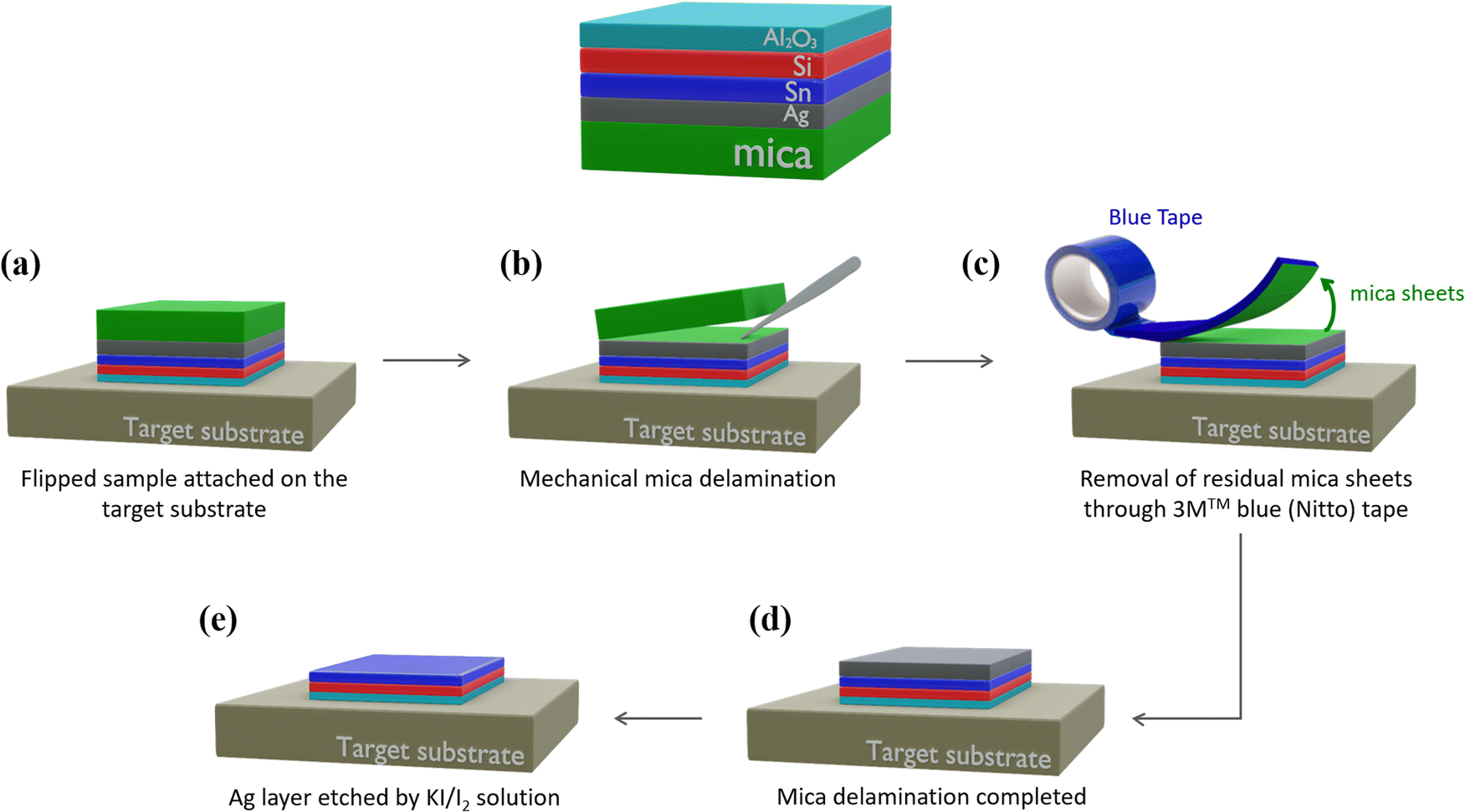 | ||
| Fig. 1 Schematic representation of the process used for transfer and delamination of the sample (from top to bottom: Al2O3 is cyan, single or multilayer silicene is red, stanene is blue, Ag is grey, and mica is green). (a) The sample is attached face-down to the target substrate, for example a metal plate. (b) A thick layer of mica is removed by using tweezers. (c) Mechanical delamination of residual mica sheets is performed with 3M™ blue Nitto tape. (d) The sample completely free of mica leaves exposed the thin Ag supporting substrate. (e) After the chemical etching of the Ag layer by KI/I2 solution, the silicene layer is protected by the AAE scheme. | ||
Fig. 2a and e present the micro-Raman spectra as a function of the silicene thickness, green (1 ML) and brown (3 MLs) lines, respectively, obtained from the (optically transparent) Al2O3 side in a backscattering configuration. Irrespective of the thickness, the Raman spectra are asymmetrical and can be decomposed in two components (see the fit to the solid curves). The primary and secondary Si peak components (dashed lines) are centred around 520 cm−1 (517 cm−1 for 1 ML, 523 cm−1 for 3 MLs, respectively) and at lower frequency (480–500 cm−1 range), respectively. The double-peak decomposition is consistent with the previously reported signature of silicene on Ag(111) (see Raman spectra for the same silicene thickness without stanene reported in Fig. S2 in the ESI†) in terms of the E2g mode of the freestanding silicene (primary peak) and buckling induced out-of-plane breathing mode(s) (secondary peak) for the single-layer silicene.23,24
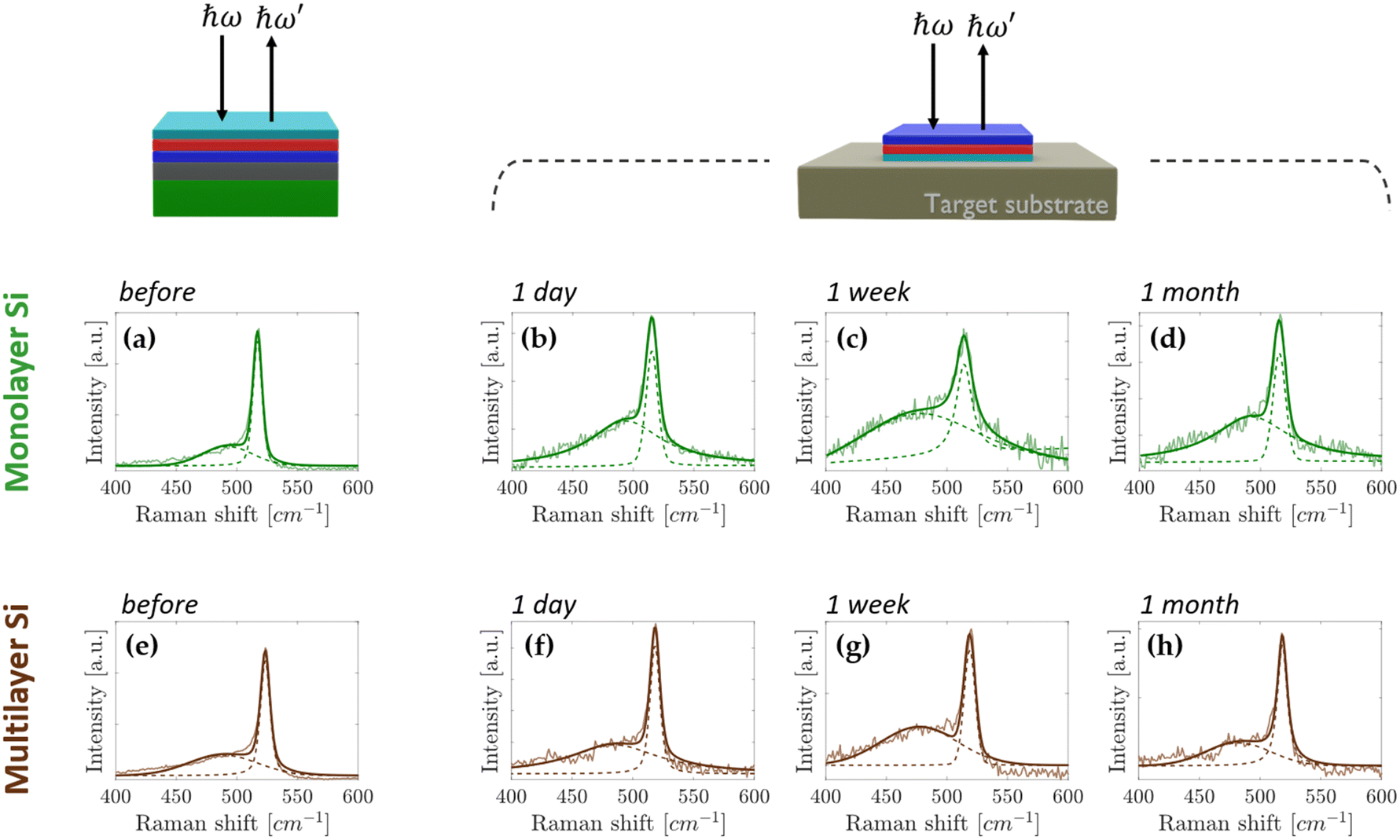 | ||
| Fig. 2 Raman spectroscopy characterization of mono (a)–(d) and multilayer (e)–(h) silicene in the AAE scheme (from top to bottom: Al2O3 is cyan, single or multilayer silicene is red, stanene is blue, silver is grey, and mica is green). (a) and (e) are the Raman spectra acquired from the top (and transparent) Al2O3 capping layer before the AAE process. (b)–(d) and (f)–(h) are the Raman spectra acquired after one day (b) and (f), one week (c)–(g), and one month (d) and (h) upon Ag removal for single and multilayer silicene, respectively. In each plot the faint curve is the raw data, the dark curve is the corresponding fitting function, and the two dashed curves show the two components used in the fitting procedure. | ||
In the case of multilayer silicene samples, the main Raman mode is blue-shifted with respect to the bulk Si(111) and the low frequency tail reconciles with the mixed sp2 and sp3 hybridization, which is ascribed to the typical hallmark of silicene when grown on Ag(111).9,12 Therefore, in both cases, these Raman signatures are considered as fingerprints of the emergence of a silicene lattice inside a silicene–stanene heterostructure consistent with the directly grown silicene. Displaying the structure of silicene via micro-Raman spectroscopy, therefore, gives us an enabling tool to monitor the silicene status during each step of the delamination process developed to prove the AAE-induced stabilization. The Al2O3-capped Xene heterostructures are flipped upside down and attached to a transfer substrate (Fig. 1a), as demonstrated by the process protocol already developed for the silicene delamination and transfer.20 Mica is stripped off with the help of a tweezer (Fig. 1b) and the remaining residues are furthermore cleaned up by using the 3M™ blue (Nitto) tape (Fig. 1c). This step is repeated until mica clearance is confirmed by close inspection through Raman spectroscopy monitoring (see Fig. S3 in ESI† for real-time monitoring during mica removal). After mica removal, the Ag substrate is etched by immersing the sample in an aqueous solution consisting of potassium iodide (KI) and iodine (I2).24 The major advantage of the modified solution is that the etching rate can be reduced down to 20 nm per minute, namely a lower amount than that reached by commercially available solutions, thus facilitating a closer control of the etching process and limiting the damage to the underlying materials. After the entire Ag layer has been etched (Fig. 1e), the layout enables us to comparatively assess the silicene stability between silicene directly grown on Ag(111) and on Sn–Ag(111). In Fig. S2 in the ESI,† we present the micro-Raman spectra obtained using the process described in Fig. 1 carried out on samples where single and multilayer silicene are directly deposited on the bare Ag(111) surface. After Ag removal, single-layer silicene starts degrading in two hours and no more silicene fingerprints can be disclosed after three hours (Fig. S2b–d, ESI†). Conversely, the stability improves significantly with the multilayer silicene, which proves to survive up to a week as shown in Fig. S2f–h of the ESI,† confirming previous reports on the longer stability of multilayer silicene.9,12 However, it should be emphasized that, after the transfer process described in Fig. 1, the acquisition of the Raman spectrum is performed on samples flipped and attached to the target substrate. During the acquisition, the underlying glue generates the fluorescence phenomenon that results in the presence of a strong background in the Raman spectrum (see Fig. S4 in ESI†).25 Since this effect does not affect the Raman spectrum of silicene and a satisfactory signal-to-noise ratio can be achieved, the so-generated background is corrected with a linear baseline during the fitting procedure, as reported in Fig. S4 in the ESI.†
Fig. 2 shows the micro-Raman spectra acquired on silicene–stanene heterostructures. Obviously, the stability before Ag removal is confirmed on a timescale comparable with that of silicene grown directly on the Ag(111) substrate without a stanene buffer layer, thus confirming the effectiveness of the Al2O3 capping layer also for the Xene heterostructures. Intriguingly, after the Ag etching through the process of Fig. 1, the differences are remarkable. Indeed, the Raman monitoring of the sample (Fig. 2b–d) makes evidence of no change in the Raman spectrum of silicene in a timescale of weeks, namely well enough to integrate silicene in a device layout with no degradation occurring.
Raman analysis was scaled up to the full area of the samples by probing differently positioned scanning points for each sample and for each time step of the time monitoring. Fig. S5 in the ESI† plots the deduced Raman shift up to one month after the Ag etching, while in Table TS1 (ESI†) the peak position values obtained by fitting and the relative intensity ratios are shown. Since the spectra of the Ag-free samples are noisier than those of non-transferred samples, the latter ones have been used as a benchmark to monitor the stability of the all-around encapsulated silicene. Fig. S6 (ESI†) shows the mean spectrum plotted with the standard deviation. Within the experimental uncertainty, the Raman shift of the monitored Raman mode can be considered unvaried thus confirming that no structural modifications occur in the sandwiched silicene. Therefore, the interfacial stanene placed in between silicene and Ag acts as a sacrificial layer that preserves the embodied silicene from oxidation and degradation. No change in the Raman spectrum was observed after three months thereby ensuring the AAE scheme as a durable stabilization strategy for silicene in a monthly timescale. Similarly, even for the multilayer silicene case, the AAE scheme proves to effectively protect the silicene film against degradation in ambient exposure for the same amount of time, as demonstrated by the Raman spectra of Fig. 2f–h and Fig. S5, S6 and Table TS1 in the ESI.†
In light of the above-mentioned findings achieved on the silicene encapsulated in between the Al2O3 capping layer and the stanene pre-deposited on Ag(111), we replaced the top capping layer, i.e., the Al2O3 thin film, with a second layer of Sn, 1 ML-thick and grown by MBE, aiming at investigating the thinnest possible AAE scheme. Hence, from top to bottom the new stacking is Sn/silicene/stanene/Ag(111). Such a configuration, where single layer silicene is embedded into two Sn layers, has been taken out of the vacuum environment for 24 hours and then re-inserted in the vacuum for X-ray photoelectron spectroscopy (XPS) investigation to determine the chemical status of the Sn/silicene/stanene stack. Fig. 3a shows the Si 2p core level (the XPS survey spectrum is shown in Fig. S7 in the ESI†) where it is possible to observe a major component related to elemental Si at binding energy (BE) of 98.77 eV with a minor component at higher-BE (101.99 eV) related to the formation of silicon oxide (SiO2).21 As already demonstrated for the Al2O3 capping layer,26 silicene can partially undergo oxidation due to inhomogeneities in the Sn capping layer likely associated with defects, or to percolation paths of the oxygen diffusion and reaction. Fig. 3b reports on the Sn 3d5/2 core level that is largely dominated by a high-BE component at 486.76 eV related to the Sn4+ oxidation state of Sn.27,28 A very small component can be found at BE = 484.77 eV being associated with the elemental Sn state.21 Interestingly this latter component is observed to increase when XPS is carried out at a take-off angle of 80° (bulk sensitive conditions, Fig. 3c) with respect to the previous 37° (surface sensitive conditions), thus suggesting that the top Sn layer is completely oxidized, whereas the bottom Sn layer (i.e., stanene, in contact with supporting Ag) is conversely in its pristine chemical status.
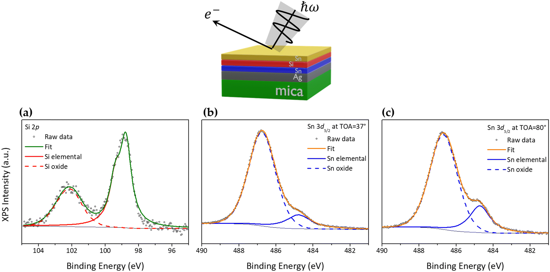 | ||
| Fig. 3 XPS analysis of the Sn/silicene/stanene on the Ag(111) configuration after exposure in ambient conditions for hours (from top to bottom: Sn is yellow, single layer silicene is red, stanene is blue, Ag is grey, and mica is green). (a) Si 2p core level where the red curve is related to the elemental Si component (including 0.63 eV doublet separation), the red dashed to the oxidized component, and the green one is the overall fit. (b) Sn 3d5/2 core level measured at the take-off angle (angle between the surface and its normal) of 37° (surface sensitive conditions), where the blue curve is related to the elemental Sn component, the blue dashed one to the oxidized component, and the orange one is the overall fit. (c) Sn 3d5/2 core level at take-off angle of 80° (bulk sensitive conditions), where the blue curve is related to the elemental Sn component, the blue dashed one to the oxidized component, and the orange one is the overall fit. | ||
Fig. 4a–d shows the ex situ micro-Raman spectroscopy plots of the single-layer silicene protected by the top Sn capping layer for up to one month. The main silicene peak undergoes no modifications throughout the Raman analysis (see also Fig. S8a in ESI†) thus demonstrating that the top Sn capping layer effectively replaces the Al2O3 in preserving the silicene fingerprints when the Sn/silicene/stanene stack configuration is under ambient conditions. Following the process scheme described in Fig. 1, the Sn/silicene/stanene stack configuration has been detached from the substrate, i.e. Ag(111) crystal on mica. Upon transferring the Sn/silicene/stanene stack onto a target substrate different from the native Ag(111) layer, we are able to obtain the thinnest configuration, limited to our survey, in which the epitaxially grown silicene has been proven to exist out of its epitaxial substrate. In Fig. 4e–h, the Raman spectroscopy analysis of the transferred Sn/silicene/stanene stack has been monitored for up to one month therein demonstrating that the main silicene Raman mode survives (see also Fig. S8b in the ESI†). Furthermore, Table TS2 in the ESI† shows the peak positions values obtained from the fitting procedure and the relative intensity ratio, while Fig. S9 (ESI†) shows the mean spectrum plotted with the standard deviation, where it can be observed that the spectra acquired after Ag etching (Fig. S9b, ESI†) are much noisier compared to the ones acquired before the processing (Fig. S9a, ESI†). As mentioned above, this is caused by the presence of glue and it is even more evident in the case of samples embedded into two Sn capping layers.
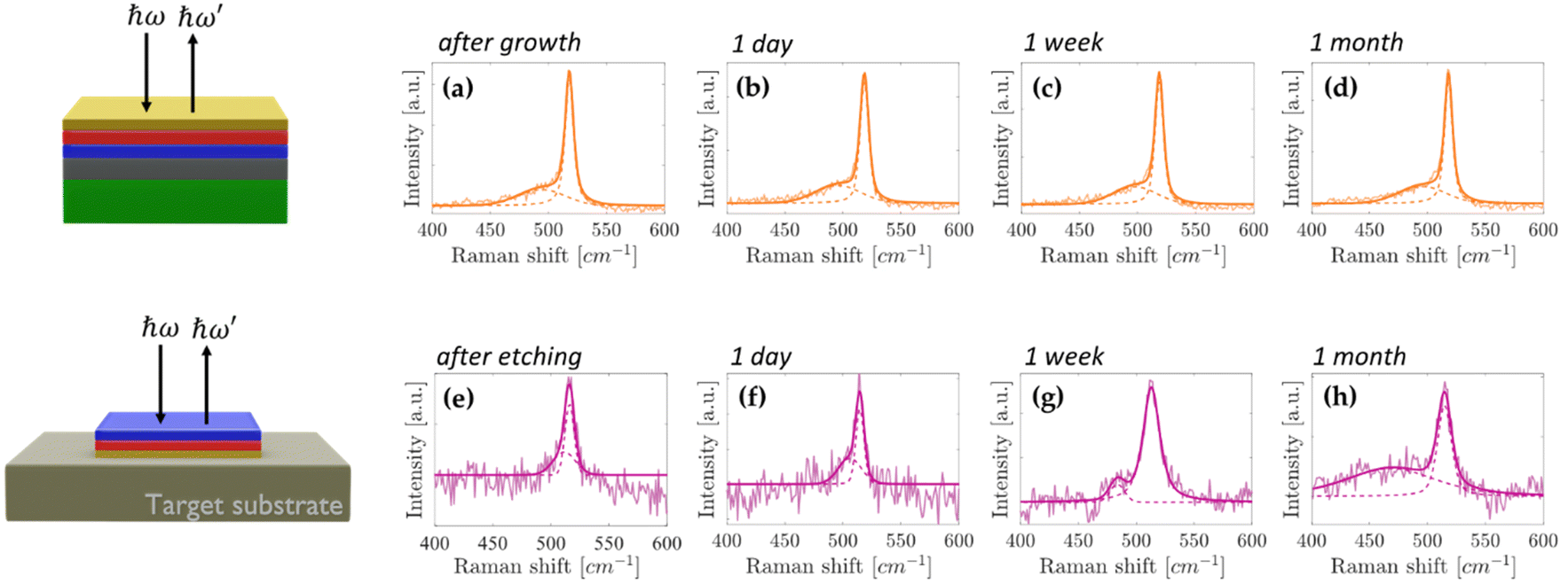 | ||
| Fig. 4 Raman spectroscopy characterization of single layer silicene embedded into two Sn capping layers (on top 1 ML Sn and at the bottom stanene grown on Ag). (a)–(d) Raman spectra monitored from the top Sn capping layer after growth with up to one month long air exposure. (e)–(h) Raman spectra monitored from the bottom Sn capping layer after sample transfer and subsequent Ag etching (as described in Fig. 1) with up to one month long air exposure. In each plot the faint curve is the raw data, the dark curve is the corresponding fit result, and the two dashed curves show the two components used in the fitting procedure. | ||
It should be noted that the Raman shift of the single-layer silicene after one month since the transfer shows the largest deviation observed after the Ag etching (3 cm−1) with respect to its pristine Raman mode. As the full-width at half-maximum is not varied, the rigid shift experienced by the Raman mode is attributed to difficulties in the baseline correction related to the reduced intensity of the Raman mode, therein posing a reasonable limit to the presented AAE scheme up to a time-scale of a month, well-beyond the time necessary to integrate silicene into operating devices.8,9
Conclusions
We demonstrate two different all-around encapsulation (AEE) schemes for the stabilization of single and multilayer silicene in ambient conditions. Both AAE schemes share the stanene on an Ag(111) template as a hosting substrate for the epitaxy of silicene. The on-top capping layer can be a thin and transparent Al2O3 film or 1 ML-thick Sn layer. In both cases, silicene, when sandwiched in between the top capping layer Al2O3/Sn and the bottom stanene, and detached from the pristine Ag(111) substrate, keeps its pristine properties as disclosed by ex situ Raman spectroscopy monitoring, thus demonstrating a superior and long-standing durability for months after being processed by virtue of the stanene as a sacrificial protective layer. These AAE schemes thus provide a further step towards the integration of silicene into operational and durable devices, overcoming the current hurdles related to its stability and processability. Finally, both AAE schemes do not depend on the Xene chemistry and therefore are expected to be extensible to Xenes other than silicene, provided that further advancements in Xene heterostructure fabrication are reached.Experimental
Samples were grown in an ultra-high vacuum Lab10 MBE system by ScientaOmicron AB with a base pressure lower than 10−10 mbar. Al (99.999% pure from Aldrich Chemistry) and Sn (99.995% pure from Goodfellow) were deposited from standard k-cells from MBE Komponenten GmbH while for Si deposition a silicon sublimator (SUSI) from the same manufacturer was used. 300 nm-thick Ag films on mica substrates are commercially available and supplied by Mateck GmbH. In order to grow single and multilayer silicene, two different surface templates are used: Ag(111) and stanene on Ag(111). The Ag(111) substrate was prepared by cycles of Ar+ sputtering followed by annealing at 550 °C, 15 minutes each. Silicene was grown using the Si sublimator keeping the substrate temperature at 225 °C. The growth rate was kept as low as 0.04 ML/s. Stanene on the Ag(111) template was realized by depositing 1.33 ML Sn on Ag(111) according to ref. 29. Before taking the samples out of the vacuum, the samples were capped with 5 nm non-reactive and amorphous Al2O3 grown at room temperature or with 1 ML Sn grown at room temperature. Ambient conditions in which the samples are exposed out of vacuum refer to 21 °C temperature and 40% humidity. Ex situ Raman spectroscopy was performed using a spectrometer equipped with a 514 nm (2.41 eV) solid state laser and a 50× (0.75 numerical aperture) objective. The incident laser power was kept below 4 mW in order to avoid sample damage, and each spectrum was acquired by collecting 3 accumulations with an exposure time of 5 seconds. The spectra were fitted with a two-component curve, using the Voigt profiles after baseline correction, as reported in Fig. S4 in the ESI.† The Ag etching solution had the following molar concentrations: [KI] = 5.13 mol L−1 and [I2] = 0.00098 mol L−1. Preparation of the solution took place under a chemical hood and the KI powder is slowly added to a becher with deionized water and stirred at room temperature. Once the powder is completely dissolved, a small amount of I2 is added, and stirring is continued for several minutes until the I2 crystals are completely dissolved.XPS was carried out in a second ultra-high vacuum system endowed with a non-monochromatized MgKα1,2 X-ray source (hν = 1253.6 eV). After Shirley background removal, the high-resolution Si 2p and Sn 3d5/2 core levels were fit by pseudo-Voigt functions (0.63 eV doublet separation is taken into account for the Si 2p core level). Surface (bulk) sensitive measurements were performed at a take-off angle of 37° (80°) between the sample surface and the hemispherical electron analyzer.
Author contributions
D. S. D. and Chi. M., contributed equally to this work. D. S. D. grew the Xene samples and carried out in situ characterization. Chr. M. and Chi. M. carried out ex situ Raman analysis. Chr. M. and Chi. M. developed process and transfer processes. C. G. performed the XPS analysis. Chr. M., C. G. and A. M. conceived, designed, and coordinated the experiments. A. M. coordinated and supervised the research, and provided and managed the technical resources. All authors contributed to the writing. All authors have given approval to the final version of the manuscript.Conflicts of interest
There are no conflicts to declare.Acknowledgements
The work is supported by EU funding from the H2020 research and innovation programme under the ERC-COG 2017 grant no. 772261 “XFab” and from the “Horizon Europe” programme under the ERC-PoC 2022 Grant No. 101069262 “XMem”. The authors thank Mario Alia and Simone Cocco (CNR-IMM) for technical support.References
- A. Molle and C. Grazianetti, Xenes – 2D Synthetic Materials Beyond Graphene, Woodhead Publishing, Elsevier, 2022 Search PubMed.
- N. R. Glavin, R. Rao, V. Varshney, E. Bianco, A. Apte, A. Roy, E. Ringe and P. M. Ajayan, Adv. Mater., 2020, 32, 1904302 CrossRef CAS PubMed.
- A. K. Tareen, K. Khan, M. Aslam, H. Zhang and X. Liu, Recent progress, challenges, and prospects in emerging group-VIA Xenes: Synthesis, properties and novel applications, Royal Society of Chemistry, 2021, vol. 13 Search PubMed.
- M. A. Kharadi, G. F. A. Malik, F. A. Khanday, K. A. Shah, S. Mittal and B. K. Kaushik, ECS J. Solid State Sci. Technol., 2020, 9, 115031 CrossRef CAS.
- T. Wang, H. Wang, K. Kui, W. Liang, X. Luo, F. Verpoort and Y. Zeng, Adv. Funct. Mater., 2020, 30, 2002885 CrossRef CAS.
- G. Shan, H. Tan, R. Ma, H. Zhao and W. Huang, Nanoscale, 2023, 15, 2982–2996 RSC.
- L. Masson and G. Prévot, Nanoscale Adv., 2023, 5, 1574–1599 RSC.
- L. Tao, E. Cinquanta, D. Chiappe, C. Grazianetti, M. Fanciulli, M. Dubey, A. Molle and D. Akinwande, Nat. Nanotechnol., 2015, 10, 227–231 CrossRef CAS PubMed.
- C. Grazianetti, E. Cinquanta, L. Tao, P. De Padova, C. Quaresima, C. Ottaviani, D. Akinwande and A. Molle, ACS Nano, 2017, 11, 3376–3382 CrossRef CAS PubMed.
- M. Lanza, Q. Smets, C. Huyghebaert and L. J. Li, Nat. Commun., 2020, 11, 1–5 CrossRef PubMed.
- P. Vogt, P. De Padova, C. Quaresima, J. Avila, E. Frantzeskakis, M. C. Asensio, A. Resta, B. Ealet and G. Le Lay, Phys. Rev. Lett., 2012, 108, 155501 CrossRef PubMed.
- P. De Padova, A. Generosi, B. Paci, C. Ottaviani, C. Quaresima, B. Olivieri, E. Salomon, T. Angot and G. Le Lay, 2D Mater., 2016, 3, 031011 CrossRef.
- H. Li, F. Hui-Xia and S. Meng, Chin. Phys. B, 2015, 24, 86102 CrossRef.
- C. Grazianetti, D. Chiappe, E. Cinquanta, G. Tallarida and M. Fanciulli, Appl. Surf. Sci., 2014, 291, 109–112 CrossRef CAS.
- P. Moras, T. O. Mentes, P. M. Sheverdyaeva, A. Locatelli and C. Carbone, J. Phys.: Condens. Matter, 2014, 26, 185001 CrossRef CAS PubMed.
- J. Genser, D. Nazzari, V. Ritter, O. Bethge, K. Watanabe, T. Taniguchi, E. Bertagnolli, F. Bechstedt and A. Lugstein, Nano Lett., 2021, 21, 5301–5307 CrossRef CAS PubMed.
- V. Ritter, J. Genser, D. Nazzari, O. Bethge, E. Bertagnolli and A. Lugstein, ACS Appl. Mater. Interfaces, 2019, 11, 12745–12751 CrossRef CAS PubMed.
- A. Molle, G. Faraone, A. Lamperti, D. Chiappe, E. Cinquanta, C. Martella, E. Bonera, E. Scalise and C. Grazianetti, Faraday Discuss., 2021, 227, 171–183 RSC.
- D. Nazzari, J. Genser, V. Ritter, O. Bethge, E. Bertagnolli, G. Ramer, B. Lendl, K. Watanabe, T. Taniguchi, R. Rurali, M. Kolíbal and A. Lugstein, J. Phys. Chem. C, 2021, 125, 9973–9980 CrossRef CAS PubMed.
- C. Martella, G. Faraone, M. H. Alam, D. Taneja, L. Tao, G. Scavia, E. Bonera, C. Grazianetti, D. Akinwande and A. Molle, Adv. Funct. Mater., 2020, 30, 2004546 CrossRef CAS.
- D. S. Dhungana, C. Grazianetti, C. Martella, S. Achilli, G. Fratesi and A. Molle, Adv. Funct. Mater., 2021, 2102797 CrossRef CAS.
- S. Achilli, D. S. Dhungana, F. Orlando, C. Grazianetti, C. Martella, A. Molle and G. Fratesi, Nanoscale, 2023, 15, 11005–11012 RSC.
- E. Cinquanta, E. Scalise, D. Chiappe, C. Grazianetti, B. Van Den Broek, M. Houssa, M. Fanciulli and A. Molle, J. Phys. Chem. C, 2013, 117, 16719–16724 CrossRef CAS.
- E. Scalise, E. Cinquanta, M. Houssa, B. Van Den Broek, D. Chiappe, C. Grazianetti, G. Pourtois, B. Ealet, A. Molle, M. Fanciulli, V. V. Afanas’Ev and A. Stesmans, Appl. Surf. Sci., 2014, 291, 113–117 CrossRef CAS.
- D. J. Gardiner and P. R. Graves, Practical Raman Spectroscopy, SpringerBerlin, Heidelberg, 1989 Search PubMed.
- A. Molle, C. Grazianetti, D. Chiappe, E. Cinquanta, E. Cianci, G. Tallarida and M. Fanciulli, Adv. Funct. Mater., 2013, 23, 4340–4344 CrossRef CAS.
- M. A. Stranick and A. Moskwa, Surf. Sci. Spectra, 1993, 2, 45–49 CrossRef CAS.
- M. A. Stranick and A. Moskwa, Surf. Sci. Spectra, 1993, 2, 50–54 CrossRef CAS.
- J. Yuhara, Y. Fuji, K. Nishino, N. Isobe, M. Nakatake, L. Xian, A. Rubio and G. Le Lay, 2D Mater., 2018, 5, 025002 CrossRef.
Footnotes |
| † Electronic supplementary information (ESI) available. See DOI: https://doi.org/10.1039/d3nh00309d |
| ‡ These authors contributed equally. |
| This journal is © The Royal Society of Chemistry 2023 |