
Solvent-assisted sulfur vacancy engineering method in MoS2 for a neuromorphic synaptic memristor†
Jiyeon
Kim‡
 a,
Changik
Im‡
b,
Chan
Lee
c,
Jinwoo
Hwang
d,
Hyoik
Jang
d,
Jae Hak
Lee
be,
Minho
Jin
b,
Haeyeon
Lee
c,
Junyoung
Kim
f,
Junho
Sung
d,
Youn Sang
Kim
*abcg and
Eunho
Lee
*d
a,
Changik
Im‡
b,
Chan
Lee
c,
Jinwoo
Hwang
d,
Hyoik
Jang
d,
Jae Hak
Lee
be,
Minho
Jin
b,
Haeyeon
Lee
c,
Junyoung
Kim
f,
Junho
Sung
d,
Youn Sang
Kim
*abcg and
Eunho
Lee
*d
aDepartment of Applied Bioengineering, Graduate School of Convergence Science and Technology, Seoul National University, Gwanak-ro 1, Gwanak-gu, Seoul 08826, Republic of Korea. E-mail: younskim@snu.ac.kr
bProgram in Nano Science and Technology, Graduate School of Convergence Science and Technology, Seoul National University, Gwanak-ro 1, Gwanak-gu, Seoul, 08826, Republic of Korea
cDepartment of Chemical and Biological Engineering, College of Engineering, Seoul National University, Gwanak-ro 1, Gwanak-gu, Seoul, 08826, Republic of Korea
dDepartment of Chemical Engineering, Kumoh National Institute of Technology, 61 Daehak-ro, Gumi-si, Gyeongsangbuk-do 39177, Republic of Korea. E-mail: leeeh@kumoh.ac.kr
eSamsung Display Company, Ltd., 1 Samsung-ro, Giheung-gu, Yongin-si, Gyeonggi-do 17113, Republic of Korea
fInspection Business Unit (IBU), Onto Innovation, 4900 W 78th St, Bloomington, MN 55435, USA
gAdvanced Institutes of Convergence Technology, Gwanggyo-ro 145, Yeongtong-gu, Suwon, 16229, Republic of Korea
First published on 2nd August 2023
Abstract
Recently, two-dimensional transition metal dichalcogenides (TMDs) such as molybdenum disulfide (MoS2) have attracted great attention due to their unique properties. To modulate the electronic properties and structure of TMDs, it is crucial to precisely control chalcogenide vacancies and several methods have already been suggested. However, they have several limitations such as plasma damage by ion bombardment. Herein, we introduced a novel solvent-assisted vacancy engineering (SAVE) method to modulate sulfur vacancies in MoS2. Considering polarity and the Hansen solubility parameter (HSP), three solvents were selected. Sulfur vacancies can be modulated by immersing MoS2 in each solvent, supported by X-ray photoelectron spectroscopy (XPS) and Raman spectroscopy analyses. The SAVE method can further expand its application in memory devices representing memristive performance and synaptic behaviors. We represented the charge transport mechanism of sulfur vacancy migration in MoS2. The non-destructive, scalable, and novel SAVE method controlling sulfur vacancies is expected to be a guideline for constructing a vacancy engineering system of TMDs.
New conceptsMany researchers are focusing on vacancy engineering in transition metal dichalcogenides (TMDs) to tune electrical properties. Several methods have already been suggested; however, there are some limitations. In case of solvent vaporization, the vaporized solvent in chemical vapor deposition (CVD) can contaminate the reactor of CVD and high temperature is required. In this study, we controlled vacancies by simply immersing the samples in three different solvents, which is termed solvent-assisted vacancy engineering (SAVE). The solvents were selected considering solubility and polarity as the two main factors. Based on the SAVE treatment, synaptic memristors were implemented and showed non-volatile memory characteristics. Facile and non-destructive SAVE method provides great potential for further investigation of TMD-based vacancy engineering. |
Introduction
Neuromorphic computing is a brain-motivated information processing model that aims to mimic the efficiency, versatility, and resilience of the human brain.1,2 To overcome the processing delay of conventional computing systems, which is called the Von Neumann bottleneck, brain computing systems have attracted widespread interest in various fields. In the human brain, numerous neurons and synapses are connected in a parallel way, and information can be delivered with low energy consumption. Artificial synapses have been developed in various structures based on these biological functionalities. In particular, memristors have attracted great attention because their low switching voltage contributes to low power consumption, which is a crucial factor in the neuromorphic system. Non-volatile resistive switching of memristors suggests applications in data storage.3–5In order to accomplish memristor representing synaptic properties, not only memristive characteristics but also synaptic plasticity and linearity need to be accompanied. First, synaptic plasticity allows the human brain to process the signals and store information simultaneously. Biological plasticity can be achieved by converting connection strength between synapses, called synaptic weight, in response to neural activities. Second, synaptic linearity can be confirmed from the shape of the long-term potentiation (LTP) and long-term depression (LTD) region. Improving linearity is essential to implementing complex neuromorphic systems. Effectively emulating the biological synaptic behaviors in electronic devices would help to meet the needs of fast and efficient neuromorphic devices.6,7
As a channel layer of synaptic memristors, transition metal dichalcogenides (TMDs) have recently emerged as ideal candidates.8–10 In particular, molybdenum disulfide (MoS2) shows outstanding performances such as high mobility (up to 1000 cm2 V−1 S−1), high on/off current ratio (∼108), and large energy bandgap (∼1.8 eV) and these properties can be easily modulated by the number of layers, thickness, and synthesis process.11 Recently, the absence of native chalcogenides (e.g., sulfur vacancies in the case of MoS2) has gained great interest because sulfur vacancies are dominantly responsible for controlling the electrical properties of TMD-based devices, such as conductance, which can result in resistive switching and memory devices.
In order to control sulfur vacancies of MoS2, several studies have adopted etching methods such as plasma, electron irradiation, and solvent vaporing, but they exhibited some limitations.12–14 Plasma treatment can physically damage the structure of MoS2 due to ion bombardment; therefore, precise vacancy modulation still remains as a problem to be solved.15,16 As a representative solvent vaporing method, chemical vapor deposition (CVD) with toluene vaporing requires a complicated and time-consuming process with high temperature, which is hard to apply for massive production. Also, contamination of the CVD reactor during solvent vaporing resulted in the degradation of equipment maintenance.17,18 In addition, most CVD-grown TMDs represented randomly distributed flakes, which is not appropriate for large-scale device applications.19 For these reasons, developing an innovative method to solve fundamental problems requires a non-destructive, scalable, and reliable fabrication process to modulate sulfur vacancies.
Herein, we present a novel solvent-assisted vacancy engineering (SAVE) method to control sulfur vacancies precisely, achieving a MoS2 synaptic memristor successfully. In particular, MoS2 was deposited by sputtering, resulting in scalable and uniform films. In previous studies, toluene has already been reported to be capable of generating sulfur vacancies in MoS2 through CVD vaporing, and the Hansen solubility parameter (HSP) of toluene was mentioned as a critical factor. Lee et al. suggested sulfur vacancy engineering by a thermal annealing process in CVD with toluene vaporing.20 However, CVD vaporing has the drawbacks of contamination in the CVD reactor and high temperature annealing around 400 °C. Instead, the novel SAVE method is a straightforward and non-destructive process, immersing MoS2 in appropriate solvents for 20 minutes at room temperature and then drying in the air without heating. Sulfur can be removed by the reaction to the solvent when MoS2 is immersed in the solvent. Thus, the SAVE method is more effective because the reaction between sulfur and solvents can directly affect generating sulfur vacancies. Since it is a solvent-assisted process, we considered solubility and polarity as two main factors in modulating sulfur vacancies. To confirm the effect of polarity, two additional solvents with similar HSP were selected, setting toluene as a standard: nonpolar chlorobenzene and bipolar tetrahydrofuran. Polarity increases from toluene to chlorobenzene and then tetrahydrofuran. In particular, the SAVE method with tetrahydrofuran resulted in the highest sulfur vacancies because the bipolar solvent is effective for removing both polar and nonpolar sulfur ions, while the nonpolar solvent is only capable of removing nonpolar sulfur ions. To sum up, we suggested a novel SAVE method to modulate sulfur vacancies considering solubility and polarity.
The SAVE method enabled us to achieve a non-destructive and uniform generation of sulfur vacancies on the MoS2 surface. Furthermore, vacancy-engineered MoS2 operated on synaptic memristors, representing both memristive characteristics and synaptic behaviors. Non-volatile memory characteristics can be explained by charge transport of sulfur vacancy migration in MoS2. Therefore, precisely controlling the vacancies in TMDs via the SAVE method would enable tuning the properties of TMDs, which can be extended to a deeper understanding of TMD-based synaptic memristors.
Results and discussion
Fig. S1 (in ESI†) illustrates the MoS2 thin film deposition and Pd/MoS2/Pd synaptic memristor fabrication process by RF sputtering, which has the advantages of large-scale and uniform MoS2 films compared to CVD-grown MoS2. Then, the samples were immersed in solvents for 20 minutes at room temperature and dried in the air. Three different solvents were selected: tetrahydrofuran, chlorobenzene, and toluene, and the samples have been termed hereafter as THF-MoS2, CB-MoS2, and TO-MoS2, corresponding to each of the solvents used. Three solvents were selected considering solubility and polarity, which will be described in detail in the next paragraph. By immersing MoS2 in solvents, sulfur can be removed due to the reaction between sulfur and the solvents, so sulfur vacancies were generated. As a result, we successfully modulated sulfur vacancies depending on different solvents, considering solubility and polarity. This fabrication process was named the solvent-assisted vacancy engineering (SAVE) method, and the detailed fabrication of a two-terminal synaptic memristor is explained in the experimental section. As shown in Fig. S2 (in ESI†), energy-dispersive X-ray spectroscopy (EDX) was conducted on a 300 μm by 300 μm scale, confirming the surface film quality and scalable uniformity of the Mo and S atoms.Analysis of sulfur vacancy modulation via the SAVE method
In previous studies, sulfur vacancies could be modulated by a CVD vaporing process but there were several limitations mentioned before. Therefore, we proposed a novel solvent-assisted method for mass production and a reliable fabrication process. In Fig. 1(a), the SAVE method controls sulfur vacancies by directly immersing MoS2 in solvents, which requires choosing an appropriate solvent with clear standards. Three solvents were used for the SAVE method, considering the solubility parameter and polarity index. According to previous studies, toluene has been a common solvent to make sulfur vacancies in MoS2, and the Hansen solubility parameter (HSP) is a key parameter for selective sulfur removal in MoS2.18 HSP can be calculated using eqn (1): | (1) |
 | ||
| Fig. 1 (a) Solvent-assisted vacancy engineering (SAVE) method with MoS2. (b) The interaction between sulfur of MoS2 and solvents. MoS2 is immersed in solvents with similar Hansen solubility parameter (HSP) but different polarity. Bipolar tetrahydrofuran (THF) makes more sulfur vacancies because it can remove both polar and nonpolar sulfur ions, while nonpolar chlorobenzene (CB) and toluene (TO) can only remove nonpolar sulfur ions. | ||
Fig. 1(b) illustrates the interaction between the sulfur of MoS2 and the solvents. There are several groups of sulfur, such as nonpolar and polar sulfur ions in MoS2, and solvents can remove unstable bonding of sulfur at the MoS2 surface when MoS2 is immersed in the solvents. It is evident that sulfur vacancies also can be strongly affected by the polarity of the solvent; therefore, we newly proposed the polarity index to confirm the polarity effect on sulfur vacancy modulation. MoS2 was treated by the SAVE method to clarify the polarity effect, using solvents with similar HSP but different polarity. The polarity index of the solvents increases from toluene (TO) to chlorobenzene (CB) and tetrahydrofuran (THF) (Table S2 in ESI†). CB has a similar property to nonpolar TO, and THF is a bipolar solvent with different properties from toluene. In particular, tetrahydrofuran is more likely to make more sulfur vacancies in MoS2 because the bipolar solvent is favorable for removing both polar and nonpolar sulfur ions, while other nonpolar solvents are only available to remove nonpolar sulfur ions.
To confirm the effect of different solvents on sulfur vacancy control, the nanostructure of the devices was further analyzed by X-ray photoelectron spectroscopy (XPS) and Raman spectroscopy (Fig. 2). Pristine-MoS2 is a film without any treatment, and others are SAVE-treated films using THF, CB, and TO, respectively. XPS spectra show that only the SAVE-treated films present a MoxSy peak, which corresponds to intermediate defect states (Fig. 2(a)). Raman spectroscopy shows that all the SAVE-treated films have larger Δk, the difference between the two-phonon modes, than the pristine-MoS2 film (Fig. 2(b)). Both analyses are clear evidence of sulfur vacancy generation by SAVE treatment.
 | ||
| Fig. 2 Confirmation of sulfur vacancy control by X-ray photoelectron spectroscopy (XPS) and Raman spectroscopy. (a) XPS Mo 3d analysis of pristine-MoS2, THF-MoS2, CB-MoS2, and TO-MoS2. Nonstoichiometric MoxSy peaks appeared in the MoS2 samples treated by the SAVE method. (b) Raman spectrum of pristine-MoS2, THF-MoS2, CB-MoS2, and TO-MoS2. (c) Areal fraction of MoxSy peaks in Mo 3d depending on solvents. (d) Raman shift (Δk) depending on solvents. Areal fraction and Raman shift increase as the polarity of the solvent increases. | ||
To be specific, as shown in Fig. 2(a), two major peaks were obtained for pristine-MoS2, and the most intense binding energy peaks occurred at 232.12 eV (Mo 3d3/2) and 228.91 eV (Mo 3d5/2), corresponding to the Mo4+ state. These values indicate the 2H-phase of MoS2 semiconducting properties.24,25 Similarly, other MoS2 samples treated by the SAVE method also showed two major peaks corresponding to the Mo4+ state, suggesting that phase transition did not occur during the SAVE method. The Mo4+ state of each solvent was observed at 233.71 eV (Mo 3d3/2) and 229.81 eV (Mo 3d5/2) for THF-MoS2, 233.77 eV (Mo 3d3/2) and 229.37 eV (Mo 3d5/2) for CB-MoS2, and 233.89 eV (Mo 3d3/2) and 229.65 eV (Mo 3d5/2) for TO-MoS2, respectively.
Unlike pristine-MoS2, non-stoichiometric MoxSy peaks with higher binding energy in the Mo 3d states were obtained for MoS2 samples treated by the SAVE method, representing the intermediate defect states.26–28 MoxSy peaks were observed near 235.88 eV and 232.07 eV for THF-MoS2, 235.39 eV and 231.55 eV for CB-MoS2, and 235.67 eV and 231.69 eV for TO-MoS2, respectively. Observation of MoxSy peaks testified that the SAVE method successfully generated sulfur vacancies for each solvent. The areal fraction of the MoxSy peaks was increased from 0% (pristine) to 23.5% (TO-MoS2), 27.9% (CB-MoS2), and 28.3% (THF-MoS2), as presented in Fig. 2(c). This result is clear evidence for effectively modulating sulfur vacancies through different solvents, and THF-MoS2 showed the highest sulfur vacancies.
Moreover, to interpret sulfur vacancies in-depth, Raman spectroscopy was conducted to support XPS analysis, as shown in Fig. 2(b). In pristine-MoS2, the Raman spectrum of the MoS2 film shows that in-plane (E12g) and out-of-plane (A1g) phonon modes of MoS2 were located at 386.59 cm−1 and 408.65 cm−1, with the difference between the two-phonon modes (Δk) of 22.06 cm−1. Two peaks of the 2H-phase of MoS2 (E12g and A1g) remained without phase change after SAVE treatment, indicating that SAVE is a non-destructive method. For other MoS2 samples by the SAVE method, the E12g and A1g mode were observed at 386.30 cm−1 and 410.68 cm−1 for THF-MoS2, 386.35 cm−1 and 410.45 cm−1 for CB-MoS2, and 386.72 cm−1 and 410.00 cm−1 for TO-MoS2, respectively. As shown in Fig. 2(d), Δk was increased from 22.06 cm−1 (pristine-MoS2) to 23.53 cm−1 (TO-MoS2), 24.03 cm−1 (CB-MoS2), and 24.38 cm−1 (THF-MoS2), indicating an increase in the out-of-plane phonon energy due to the sulfur defects.24,25 Previous studies reported that the sulfur deficient MoS2 weakened the restoring force and allowed the Mo atom to vibrate out-of-plane. As a result, A1g was blue-shifted, and the phonon energy increased, consistent with the sulfur vacancy generation.29,30 Also, sulfur vacancies increase as Δk increases, so the Raman spectrum shows the same tendency as the XPS results, indicating precise sulfur vacancy modulation depending on the polarity of the solvents.30
To sum up, sulfur vacancies were modulated successfully by the SAVE method based on similar HSP and polarity indexes. XPS and Raman spectrum analyses support that sulfur vacancies increase as the polarity index of the solvent increases, indicating that THF-MoS2 shows the highest sulfur vacancies.
Memristive performance of the THF-MoS2 synaptic memristor
To compare pristine-MoS2 and vacancy-engineered MoS2 by the SAVE method, we fabricated two-terminal devices and measured their electrical performances. Fig. 3(a) illustrates the vertical structure of the Pd/MoS2/Pd synaptic memristor on the Si/SiO2 substrate. As shown in the image acquired by cross-sectional transmission electron microscopy (TEM), it was confirmed that the deposited MoS2 film had a thickness of 5 nm and a sharp interface to encourage charge injection effectively between the top and bottom electrodes. | ||
| Fig. 3 Memristive performance of the pristine and SAVE-treated MoS2 synaptic memristor. (a) A schematic of the MoS2 device structure and cross-sectional transmission electron microscopy (TEM) image on the Si/SiO2 substrate. (b) I–V curve of pristine-MoS2 without the memristive effect. I–V curve of (c) THF-MoS2, (d) CB-MoS2, and (e) TO-MoS2 with bipolar resistive switching. (f) The measured conductance at HRS and LRS maintained for 104 s of retention test. (g) The measured conductance of the THF-MoS2 synaptic memristor at HRS and LRS maintained for 100 cycles. (h) The histogram of VSET and VRESET from 49 THF-MoS2 memristors. | ||
Pristine-MoS2 and SAVE-treated MoS2 synaptic memristors were measured. In the pristine-MoS2 synaptic memristor, the electrical I–V curve did not show a hysteresis window meaning memristive effects as the pristine MoS2 lacked sulfur vacancies (Fig. 3(b)). On the other hand, all SAVE-treated synaptic memristors exhibited non-volatile characteristics with two distinct behaviors of high resistance state (HRS) and low resistance state (LRS), as shown in Fig. 3(c)–(e). THF-MoS2 and CB-MoS2 have bigger Ion/Ioff than TO-MoS2, and THF-MoS2 has lower VSET (SET voltage), and VRESET (RESET voltage) than CB-MoS2 and TO-MoS2 (Table S3 in ESI†). By comparing the I–V curves with the three different solvents, the THF-MoS2 synaptic memristor showed the best performance. Prior to the voltage sweep on the THF-MoS2 synaptic memristor, a small amount of current flow (∼100 nA) was observed in HRS. The current increased by approximately 102 times in LRS after the SET process (VSET ∼ 1.25 V), and sequential current decrement evoked the RESET process when a negative voltage was applied (VRESET ∼ −1.28 V).
The voltage sweep was performed repeatedly to verify the stability of the THF-MoS2 synaptic memristor. The conductance was measured simultaneously with the DC sweep varying from −2 V to 2 V. The retention time of HRS and LRS was measured to examine the stability of the devices over time as well as the overall electrical stability. After the SET and RESET process, 0.1 V of Vread (read voltage) was applied for 104 s for LRS and HRS, respectively. The interval data point is 10 s (Fig. 3(f)). In Fig. 3(g), the conductance measured from the HRS and LRS was 3.57 ± 0.89 × 10⁻⁷ S and 8.76 ± 0.51 × 10⁻⁶ S, respectively, and maintained for 100 cycles. Also, the cycling test of the CB-MoS2 and TO-MoS2 synaptic memristor was maintained for 100 cycles (Fig. S3 in ESI†), but the THF-MoS2 synaptic memristor was more stable than the CB-MoS2 and TO-MoS2 synaptic memristors. Based on the aforementioned electrical measurements, it was observed that the sulfur vacancies generated by the SAVE method were well maintained and operated in the MoS2 film.
In addition, THF-MoS2 synaptic memristors exhibited high uniformity and reliability. Fig. 3(h) shows the VSET and VRESET of the 49 devices on the Si/SiO2 substrate. The average values of VSET and VRESET obtained from the histogram were 1.18 V (± 0.11 V) and −1.26 V (± 0.10 V), respectively. Additionally, the distribution of the Ion/Ioff of the 49 devices was examined (Fig. S4 in ESI†). The average Ion/Ioff was 1.34 × 10², and it was confirmed that the overall performance of 49 devices was consistent. Furthermore, the I–V curves of the THF-MoS2 synaptic memristor were uniform for 30 cycles, verifying repeatability (Fig. S5 in ESI†). Therefore, the THF-MoS2 synaptic memristor showed high uniformity and reliability due to the consistent interaction between MoS2 and the solvents.
Charge transport mechanism in vacancy-engineered MoS2 as a memory-device operation
In order to confirm the memristive effect of the vacancy-engineered MoS2 synaptic memristor, which modulates sulfur vacancies via the SAVE method, it is necessary to represent a reasonable charge transport mechanism. The I–V curve of the MoS2 synaptic memristor in HRS was fitted into ln(I/V) versus V1/2, as shown in Fig. 4(a). The fitted line follows Poole–Frenkel (P–F) transport, demonstrating that sulfur vacancies act as localized states where electrons are trapped. The P–F model shows a linear relation between ln(I/V) and V1/2, and it is dominant after V > 0.5 V because injected carriers in the MoS2 channel became thermally activated.31–33 In the case of LRS, on applying a voltage sweep during the SET process, sulfur vacancies migrate in MoS2, which is consistent with the previously reported studies.4,34–36 As a result, decreased electrical resistance caused an increment in the current level. This SET process was fitted into a double logarithmic curve of I versus V, showing ohmic behavior. The slope value was unity, suggesting a consistent relationship with Ohm's law (V = I·R), as shown in Fig. 4(b).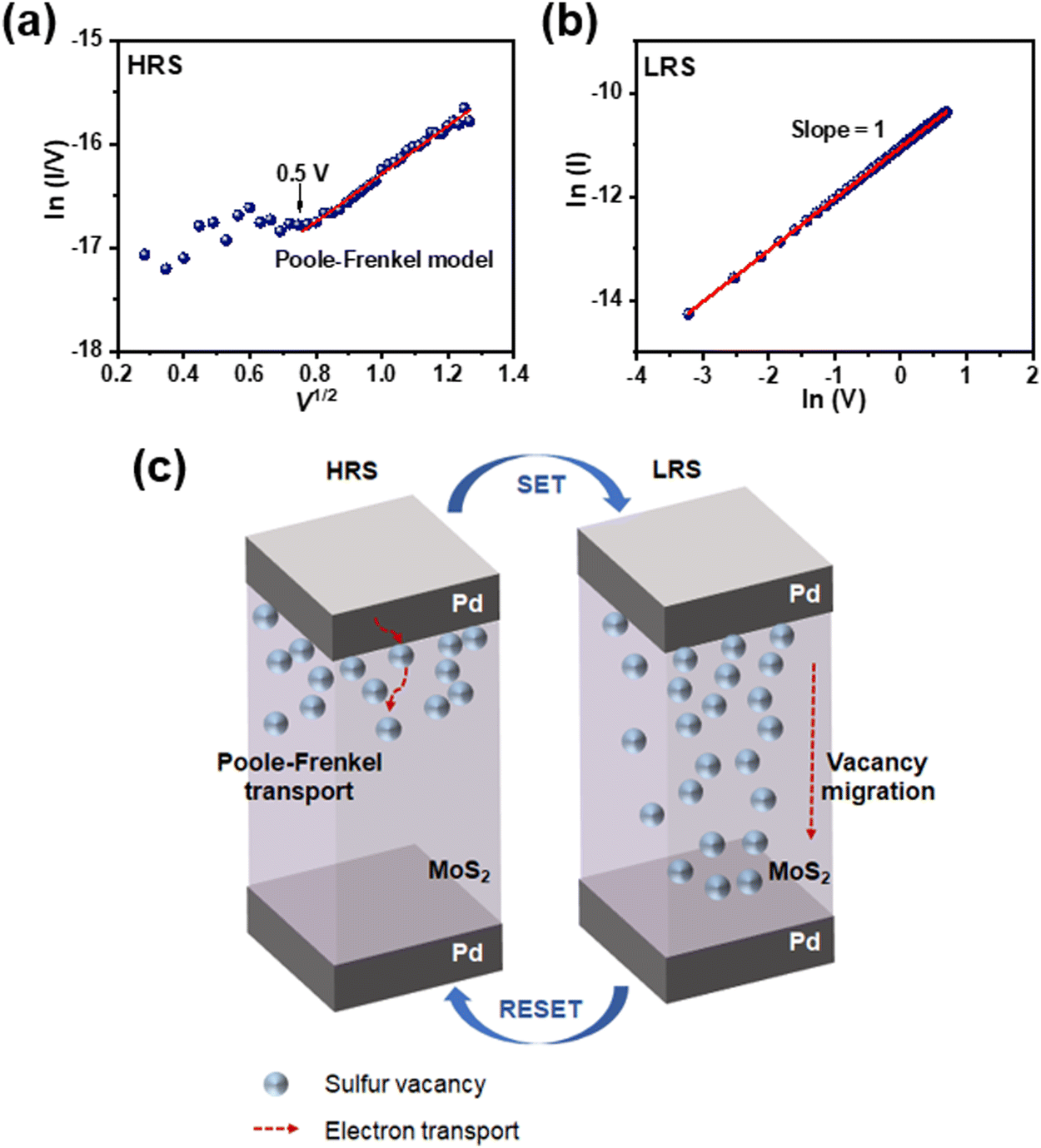 | ||
| Fig. 4 Charge transport mechanism in vacancy-engineered MoS2 as a memory-device operation. Memristive characteristics of the THF-MoS2 fitted into (a) the Poole–Frenkel (P–F) model in HRS and (b) Ohm's law in LRS. (c) An illustration of the charge transport mechanism in HRS (left) and LRS (right) through sulfur vacancy migration. | ||
Fig. 4(c) illustrates the charge transport mechanism of memory-device operation in the vacancy-engineered MoS2 synaptic memristor. In HRS, vacancy migration hardly occurs; thus, current flow in HRS can be illustrated by electron hopping through sulfur vacancies.37 Otherwise, sulfur vacancies started the migration in LRS, and the charged electrons were then transported when sufficient voltage was applied to the two Pd electrodes. At the SET process, the current increased because sulfur vacancies migrate and metallic transport was observed. On the other hand, when a negative voltage sweep was applied at the RESET process, vacancies cannot migrate and the current decreased.37
Synaptic behaviors of the THF-MoS2 synaptic memristor
Due to the non-volatile memory characteristics, memristors with resistive switching from HRS to LRS are able to mimic the biological nerve system of synaptic linearity and plasticity, which can be implemented in brain-inspired artificial synapses.38–42 In the human brain, electrical signals are converted into the form of ions such as Ca2+, K+, and Na+. Neurotransmitters are triggered and deliver information from presynaptic to postsynaptic neurons, as shown in Fig. 5(a). To emulate the short-term plasticity of the biological synapse, two consecutive voltage pulses were applied to the drain terminal as a presynaptic input while the drain–source current was continuously recorded as a postsynaptic current. Fig. 5(b) shows the electrical response of the THF-MoS2 synaptic memristor as double pulses (V = 1 V) were applied. The electrical signal was enhanced from 40.7 nS to 43.3 nS, and gradually up to 44.6 nS.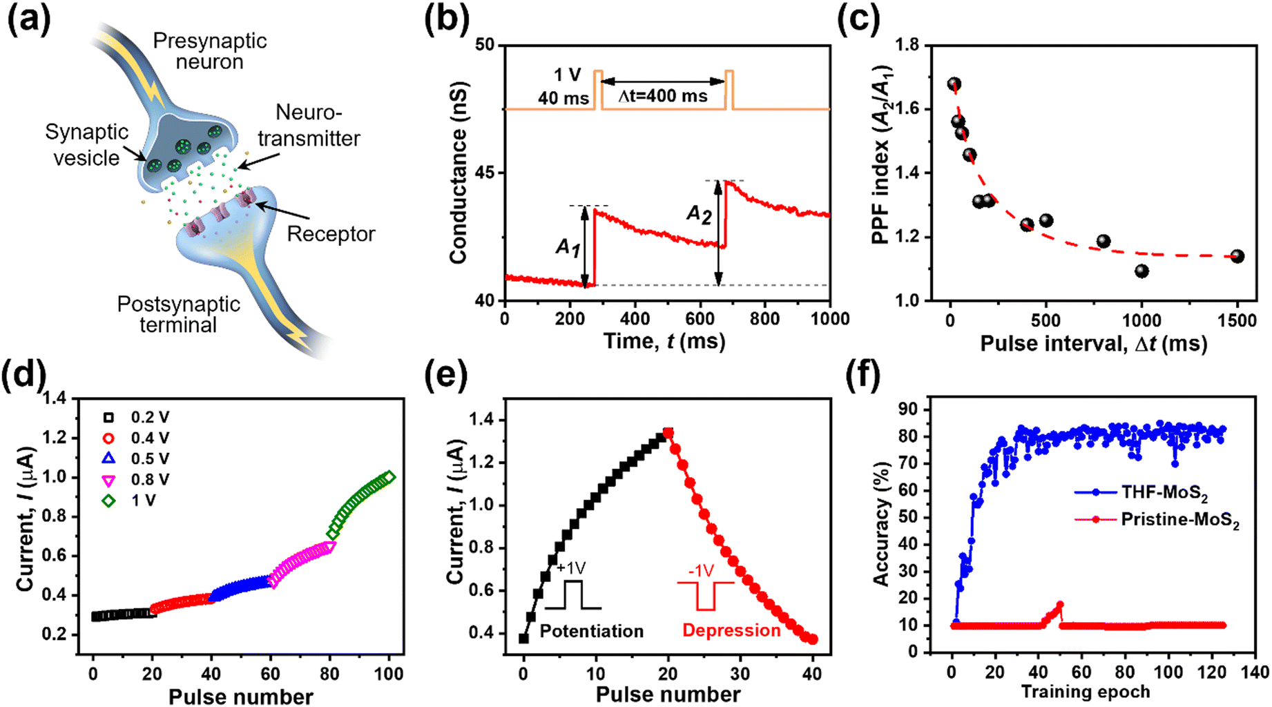 | ||
| Fig. 5 Synaptic behaviors of the THF-MoS2 synaptic memristor. (a) A schematic diagram of a biological synapse. (b) Short-term plasticity by conductance changes with double pulses. (c) PPF index −Δt curve by varying intervals between consecutive pulses. (d) Postsynaptic currents change depending on pulse amplitude from 0.2 V to 1 V. (e) A demonstration of LTP/LTD behaviors when 20 successive voltages are applied (VLTP = +1 V for 20 ms, VLTD = −1 V for 20 ms). (f) The recognition accuracy of THF-MoS2 and pristine-MoS2 by MNIST training. | ||
The time width (tw) was 40 ms and the time interval (Δt) of each pulse was 400 ms. In Fig. 5(c), paired-pulse facilitation (PPF) is one of the indexes representing short-term plasticity depending on the ratio of two series of pulses with short time intervals, which can be defined as eqn (2):
 | (2) |
Linearity is also a significant index representing the degree of conductance change caused by the consecutive pulses, which can be illustrated in two separate sections: long-term potentiation (LTP) and long-term depression (LTD).44 When 20 successive positive voltages (V = +1 V, tw = 20 ms, and Δt = 200 ms) and 20 successive negative voltages (V = −1 V, tw = 20 ms, and Δt = 200 ms) are applied to the THF-MoS2 synaptic memristor, LTP and LTD can be shown as Fig. 5(e), confirming the synaptic behavior.45,46 To evaluate synaptic performance, the linearity in the region of LTP and LTD of the THF-MoS2 synaptic memristor and pristine-MoS2 were evaluated using eqn (3)–(5):
 | (3) |
 | (4) |
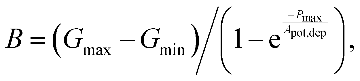 | (5) |
Modified National Institute of Standards and Technology (MNIST) training was conducted based on calculated linearity (Fig. 5(f)). The recognition accuracy of the THF-MoS2 synaptic memristor was about 85.03% after 40 training epochs, while that of pristine-MoS2 remained 9.8% for 125 training epochs, rarely showing learning ability. The SAVE method was verified as an effective technique for MoS2 synaptic memristors showing a high recognition accuracy and great linearity.
Visual simulation of the THF-MoS2 synaptic memristor
Fig. 6 is a visual simulation of the THF-MoS2 synaptic memristor under the potentiation process (V = 1 V) and depression process (V = −1 V) with a series of 20 pulses to represent memorizing/forgetting processes.47 LTP is represented when synaptic weight is increased, improving data storage capacity. On the contrary, LTD is represented when synaptic weight is decreased, which results in forgetting the stored information. For the image recognition process in 160 × 160 pixels, a real architecture image is coded by the current of different pulse numbers. Images were simulated in three-step with pulse numbers of 3, 10, and 18 and painted with the color bar of normalized current from 0 to 1. Based on the data in Fig. 5(e), normalized current values of LTP increased to 0.49, 0.77, and 0.96 and those of LTD decreased to 0.82, 0.51, and 0.30 (Table S4 in ESI†). The architecture image shows visual memorization under the potentiation process (Fig. 6(a)). As the pulse number increased in the potentiation process, the image became darker, which means the current increased gradually. In contrast, visual forgetting was observed during the depression process showing a faded image resulting from the current decrease from pulse number 3 to pulse number 18 (Fig. 6(b)). The visual simulation clearly represented the memorizing/forgetting process by potentiation/depression and can be considered an example of emulating synaptic behaviors.48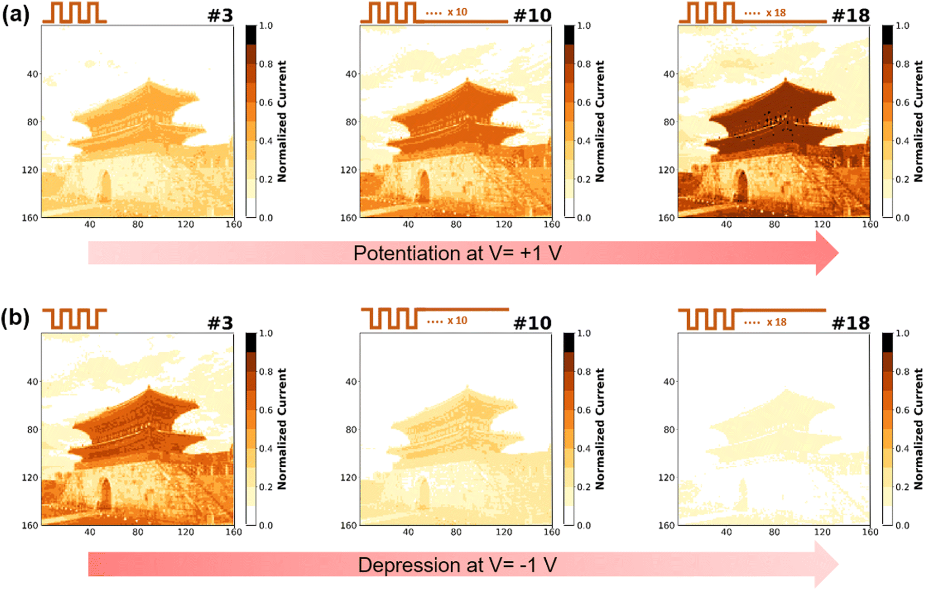 | ||
| Fig. 6 Visual simulation of the THF-MoS2 synaptic memristor under potentiation and depression processes. The real image of the architecture is coded by the current of different pulse numbers in 160 × 160 pixels. (a) Visual memorization of the synaptic memristor under a potentiation process (V = 1 V) when the pulse number is #3, #10, and #18. (b) Visual forgetting of the synaptic memristor under a depression process (V = −1 V) when the pulse number is #3, #10, and #18. | ||
Conclusions
In summary, we proposed a facile, non-destructive, and scalable SAVE method to modulate sulfur vacancies in sputtered MoS2, and solubility and polarity are considered as two main factors. In particular, the polarity effect on sulfur vacancy modulation was confirmed by variation in the polarity of the solvent. When solvents have similar HSP, the bipolar solvent is favorable for generating sulfur vacancies because it can remove both polar and nonpolar sulfur, which is effective for generating sulfur vacancies. The results and tendency of XPS and Raman analyses are obvious evidence of sulfur vacancy modulation. Also, sulfur vacancy migration was proposed for the mechanism of the SAVE-treated MoS2 synaptic memristor. Among the three solvents, the THF-treated MoS2 synaptic memristor showed the best performance due to its highest sulfur vacancies. The THF-MoS2 synaptic memristor represented non-volatile characteristics of programming/erasing current ratio (>102) and long retention (>104 s), and synaptic behaviors of PPF of about 170% and 8 times increased linearity. MNIST and visual imaging simulation conducted neuromorphic computing to support these characteristics. We proposed the SAVE method to control vacancies in TMDs, and this is a novel study to our knowledge. The SAVE method accomplished a concise, non-destructive, and reliable process and provided the framework for further investigations to suggest TMD-based electronic devices for application in both academic and industrial fields.Methods
MoS2 thin film deposition and device fabrication
Four steps were taken in order to fabricate a MoS2 synaptic memristor. First, a 300 nm thick Si/SiO2 substrate was cleaned and rinsed using acetone, isopropyl alcohol, and distilled water. Second, the Si/SiO2 substrate was placed into the vacuum chamber (10−6 Torr) of the RF/DC sputtering system. Third, a bottom electrode, Pd, was linearly patterned and DC sputtered on a Si/SiO2 substrate via Ar plasma (99.99% Airgas). The deposition power and time were set at 60 W for 3 min. Fourth, after bottom electrode deposition, the MoS2 target was RF sputtered over the Pd deposited substrate at 60 W for 2 min. Lastly, Pd was perpendicularly patterned as a top electrode, and DC sputtered on top of the MoS2 film.Solvent immersion
Three different solvents, toluene (Sigma Aldrich, anhydrous, 99.8%), chlorobenzene (Alfa Aesar, ACS grade, 99.5%), and tetrahydrofuran (Sigma Aldrich, anhydrous, 99.9%) were purchased and used for the SAVE method. After MoS2 deposition via sputtering, the samples were immersed in 3 ml of each solvent for 20 min and then dried in the air.Electrical characterizations
The I–V properties of the MoS2 synaptic memristors were characterized at room temperature in the ambient environment via an Agilent B2900A by applying DC and pulse voltage in a probestation (MSTECH MST4000A).Materials characterization
The crystalline properties of MoS2 were analyzed using Raman spectroscopy (uninanotech UniRAM-7000). The thickness and electrochemical properties of the samples were measured using Atomic Force Microscopy (Parks NX-10). The atomic composition and distribution were analyzed using X-ray Photoelectron Spectroscopy (PHI 5000 Versa Probe Scanning XPS). TEM characterizations were analyzed using a JSM-7800F Prime instrument (JEOL. Ltd) at an operational voltage of 200 kV, which was fitted with a Cs corrector (CEOS GmbH) and FEG-STEM/TEM unit.Conflicts of interest
There are no conflicts to declare.Acknowledgements
This research was supported by the Basic Science Research Program through the National Research Foundation of Korea (NRF), funded by the Ministry of Science & ICT (2022R1C1C1010319 and RS-2023-00208273). The authors acknowledge the support from the Commercialization Promotion Agency for R&D Outcomes (COMPA) funded by the Ministry of Science and ICT (MSIT) (2022-URE-03). This research was also supported by the Korea Institute for Advancement of Technology (KIAT) grant funded by the Korea Government (P0012451, The Competency Development Program for Industry Specialist). J. K. acknowledges the illustration support from Noah Studio LLC.References
- P. A. Merolla, J. V. Arthur, R. Alvarez-Icaza, A. S. Cassidy, J. Sawada, F. Akopyan, B. L. Jackson, N. Imam, C. Guo, Y. Nakamura, B. Brezzo, I. Vo, S. K. Esser, R. Appuswamy, B. Taba, A. Amir, M. D. Flickner, W. P. Risk, R. Manohar and D. S. Modha, Science, 2014, 345, 668–673 CrossRef CAS PubMed.
- M. A. Zidan, J. P. Strachan and W. D. Lu, Nat. Electron., 2018, 1, 22–29 CrossRef.
- K. Sun, J. Chen and X. Yan, Adv. Funct. Mater., 2021, 31, 2006773 CrossRef CAS.
- W. Sun, B. Gao, M. Chi, Q. Xia, J. J. Yang, H. Qian and H. Wu, Nat. Commun., 2019, 10, 3453 CrossRef PubMed.
- Q. Liang, Q. Zhang, X. Zhao, M. Liu and A. T. S. Wee, ACS Nano, 2021, 15, 2165–2181 CrossRef CAS PubMed.
- Q. Zhao, Z. Xie, Y.-P. Peng, K. Wang, H. Wang, X. Li, H. Wang, J. Chen, H. Zhang and X. Yan, Mater. Horiz., 2020, 7, 1495–1518 RSC.
- L. Zhou, S. Yang, G. Ding, J.-Q. Yang, Y. Ren, S.-R. Zhang, J.-Y. Mao, Y. Yang, Y. Zhou and S.-T. Han, Nano Energy, 2019, 58, 293–303 CrossRef CAS.
- S. Bertolazzi, P. Bondavalli, S. Roche, T. San, S.-Y. Choi, L. Colombo, F. Bonaccorso and P. Samorì, Adv. Mater., 2019, 31, 1806663 CrossRef PubMed.
- W. Huh, D. Lee and C.-H. Lee, Adv. Mater., 2020, 32, 2002092 CrossRef CAS PubMed.
- G. Lee, J.-H. Baek, F. Ren, S. J. Pearton, G.-H. Lee and J. Kim, Small, 2021, 17, 2100640 CrossRef CAS PubMed.
- C. Mihai, F. Sava, A. C. Galca and A. Velea, AIP Adv., 2020, 10, 025102 CrossRef CAS.
- S. Roy, W. Choi, S. Jeon, D.-H. Kim, H. Kim, S. J. Yun, Y. Lee, J. Lee, Y.-M. Kim and J. Kim, Nano Lett., 2018, 18, 4523–4530 CrossRef CAS PubMed.
- Y. Lee, G. Ghimire, S. Roy, Y. Kim, C. Seo, A. K. Sood, J. I. Jang and J. Kim, ACS Photonics, 2018, 5, 2904–2911 CrossRef CAS.
- S. Wang, G.-D. Lee, S. Lee, E. Yoon and J. H. Warner, ACS Nano, 2016, 10, 5419–5430 CrossRef CAS PubMed.
- W. S. Seo, D. K. Kim, J.-H. Han, K.-B. Park, S. C. Ryu, N. K. Min and J. H. Kim, Nanomaterials, 2020, 10, 1860 CrossRef CAS PubMed.
- A.-Y. Lu, X. Yang, C.-C. Tseng, S. Min, S.-H. Lin, C.-L. Hsu, H. Li, H. Idriss, J.-L. Kuo, K.-W. Huang and L.-J. Li, Small, 2016, 12, 5530–5537 CrossRef CAS PubMed.
- J. Kim, E. Lee, G. Mehta and W. Choi, Nanotechnology, 2020, 31, 445203 CrossRef CAS PubMed.
- W. Choi, J. Kim, E. Lee, G. Mehta and V. Prasad, ACS Appl. Mater. Interfaces, 2021, 13, 13596–13603 CrossRef CAS PubMed.
- N. Choudhary, M. D. Patel, J. Park, B. Sirota and W. Choi, J. Mater. Res., 2016, 31, 824–831 CrossRef CAS.
- E. Lee, J. Kim, J. Park, J. Hwang, H. Jang, K. Cho and W. Choi, ACS Appl. Mater. Interfaces, 2023, 15, 15839–15847 CrossRef CAS PubMed.
- K.-G. Zhou, N.-N. Mao, H.-X. Wang, Y. Peng and H.-L. Zhang, Angew. Chem., Int. Ed., 2011, 50, 10839–10842 CrossRef CAS PubMed.
- J. N. Coleman, M. Lotya, A. O’Neill, S. D. Bergin, P. J. King, U. Khan, K. Young, A. Gaucher, S. De, R. J. Smith, I. V. Shvets, S. K. Arora, G. Stanton, H.-Y. Kim, K. Lee, G. T. Kim, G. S. Duesberg, T. Hallam, J. J. Boland, J. J. Wang, J. F. Donegan, J. C. Grunlan, G. Moriarty, A. Shmeliov, R. J. Nicholls, J. M. Perkins, E. M. Grieveson, K. Theuwissen, D. W. McComb, P. D. Nellist and V. Nicolosi, Science, 2011, 331, 568–571 CrossRef CAS PubMed.
- C. M. Hansen, Hansen Solubility Parameters: A User's Handbook, 2nd edn, CRC press, 2007 Search PubMed.
- S. Bhoyate, J. Kim, E. Lee, B. Park, E. Lee, J. Park, S. H. Oh, J. Kim and W. Choi, J. Mater. Chem. A, 2020, 8, 12436–12445 RSC.
- S. Bhoyate, S. Mhin, J. Jeon, K. Park, J. Kim and W. Choi, ACS Appl. Mater. Interfaces, 2020, 12, 27249–27257 CrossRef CAS PubMed.
- N. P. Kondekar, M. G. Boebinger, E. V. Woods and M. T. McDowell, ACS Appl. Mater. Interfaces, 2017, 11 Search PubMed.
- M. A. Baker, R. Gilmore, C. Lenardi and W. Gissler, Appl. Surf. Sci., 1999, 150, 255–262 CrossRef CAS.
- J. Lee, J. Heo, H. Y. Lim, J. Seo, Y. Kim, J. Kim, U. Kim, Y. Choi, S. H. Kim, Y. J. Yoon, T. J. Shin, J. Kang, S. K. Kwak, J. Y. Kim and H. Park, ACS Nano, 2020, 14, 17114–17124 CrossRef CAS PubMed.
- K. Wu, Z. Li, J. Tang, X. Lv, H. Wang, R. Luo, P. Liu, L. Qian, S. Zhang and S. Yuan, Nano Res., 2018, 11, 4123–4132 CrossRef CAS.
- W. M. Parkin, A. Balan, L. Liang, P. M. Das, M. Lamparski, C. H. Naylor, J. A. Rodríguez-Manzo, A. T. C. Johnson, V. Meunier and M. Drndić, ACS Nano, 2016, 10, 4134–4142 CrossRef CAS PubMed.
- S. Liu, Y. Sun, B. Song, Z. Li, H. Liu and Q. Li, Phys. Lett. A, 2019, 383, 125877 CrossRef CAS.
- M. J. M. Jimenez, R. F. de Oliveira, F. M. Shimizu, C. C. B. Bufon, V. Rodrigues, Â. L. Gobbi, M. H. O. Piazzetta and A. Riul, Nanotechnology, 2018, 29, 505703 CrossRef PubMed.
- E. W. Lim and R. Ismail, Electronics, 2015, 4, 586–613 CrossRef CAS.
- Y. Sun, X. Yan, X. Zheng, Y. Liu, Y. Zhao, Y. Shen, Q. Liao and Y. Zhang, ACS Appl. Mater. Interfaces, 2015, 7, 7382–7388 CrossRef CAS PubMed.
- A. Kumar, M. Das, V. Garg, B. S. Sengar, M. T. Htay, S. Kumar, A. Kranti and S. Mukherjee, Appl. Phys. Lett., 2017, 110, 253509 CrossRef.
- V. K. Sangwan, D. Jariwala, I. S. Kim, K.-S. Chen, T. J. Marks, L. J. Lauhon and M. C. Hersam, Nat. Nanotechnol., 2015, 10, 403–406 CrossRef CAS PubMed.
- Y. Yang, H. Du, Q. Xue, X. Wei, Z. Yang, C. Xu, D. Lin, W. Jie and J. Hao, Nano Energy, 2019, 57, 566–573 CrossRef CAS.
- Y. Shi, X. Liang, B. Yuan, V. Chen, H. Li, F. Hui, Z. Yu, F. Yuan, E. Pop, H.-S. P. Wong and M. Lanza, Nat. Electron., 2018, 1, 458–465 CrossRef.
- X. Yan, Z. Zhou, B. Ding, J. Zhao and Y. Zhang, J. Mater. Chem. C, 2017, 5, 2259–2267 RSC.
- N. Lu, L. Li, P. Sun, M. Wang, Q. Liu, H. Lv, S. Long and M. Liu, J. Phys. D: Appl. Phys., 2015, 48, 065101 CrossRef CAS.
- M. Jin, H. Lee, J. H. Lee, D. Han, C. Im, J. Kim, M. Jeon, E. Lee and Y. S. Kim, Appl. Phys. Rev., 2023, 10, 011407 CAS.
- R. S. Zucker and W. G. Regehr, Annu. Rev. Physiol., 2002, 64, 355–405 CrossRef CAS PubMed.
- L. Fang, S. Dai, Y. Zhao, D. Liu and J. Huang, Adv. Electron. Mater., 2020, 6, 1901217 CrossRef CAS.
- C. Im, J. Kim, J. H. Lee, M. Jin, H. Lee, J. Lee, J. C. Shin, C. Lee, Y. S. Kim and E. Lee, J. Appl. Phys., 2022, 132, 044503 CrossRef CAS.
- M.-K. Kim, I.-J. Kim and J.-S. Lee, Appl. Phys. Lett., 2021, 118, 032902 CrossRef CAS.
- S.-M. Kim, S. Kim, L. Ling, S. E. Liu, S. Jin, Y. M. Jung, M. Kim, H.-H. Park, V. K. Sangwan, M. C. Hersam and H.-S. Lee, ACS Appl. Mater. Interfaces, 2022, 14, 5673–5681 CrossRef CAS PubMed.
- H. Lee, M. Jin, H.-J. Na, C. Im, J. H. Lee, J. Kim, Y. J. Gong, C. Lee, E. Lee and Y. S. Kim, Adv. Funct. Mater., 2022, 32, 2110591 CrossRef CAS.
- S. Hong, H. Cho, B. H. Kang, K. Park, D. Akinwande, H. J. Kim and S. Kim, ACS Nano, 2021, 15, 15362–15370 CrossRef CAS PubMed.
Footnotes |
| † Electronic supplementary information (ESI) available. See DOI: https://doi.org/10.1039/d3nh00201b |
| ‡ J. K. and C. I. contributed equally to this work |
| This journal is © The Royal Society of Chemistry 2023 |