
Performance and stability enhancement of perovskite photodetectors by additive and interface engineering using a dual-functional PPS zwitterion†
Abbas Ahmad
Khan
 a,
Navneet
Kumar
a,
Uijin
Jung
a,
Wonjun
Heo
b,
Zhaozhong
Tan
a and
Jinsub
Park
*ab
a,
Navneet
Kumar
a,
Uijin
Jung
a,
Wonjun
Heo
b,
Zhaozhong
Tan
a and
Jinsub
Park
*ab
aDepartment of Electronic Engineering, Hanyang University, Seoul 04763, Republic of Korea. E-mail: jinsubpark@hanyang.ac.kr
bDivision of Nanoscale Semiconductor Engineering, Hanyang University, Seoul 04763, Republic of Korea
First published on 5th September 2023
Abstract
Hybrid organic–inorganic metal halide perovskites (HOIPs) have gained significant research interest due to their tunable optoelectronic properties and ease of fabrication. Enhancing the stability and efficiency of perovskite materials can be achieved through the passivation of defective surfaces and the improvement of interfacial properties. In this study, we introduce a zwitterionic compound, PPS (3-(1-pyridinio)-1-propanesulfonate), as a bifunctional material that serves as an additive and an interlayer. Incorporating PPS into the perovskite film effectively reduces both positively and negatively charged defects, leading to improved surface morphology and a reduction in undesired charge carrier recombination. Additionally, the formation of a PPS interlayer on SnO2 improves the SnO2/perovskite interfacial characteristics, thereby enhancing charge carrier extraction. As a result, the photodetector exhibits a low dark current of 6.05 × 10⁻¹¹ A, an excellent responsivity of 5.93 A W−1, a detectivity of 1.51 × 10¹³ J, and an on/off ratio of 1.2 × 10⁴ under open-air conditions. Moreover, the device demonstrates outstanding stability, retaining 80% of its original responsivity in an ambient environment. This work highlights the great potential of dual-functional materials for defect passivation in future optoelectronic devices, emphasizing the importance of surface modification and interface engineering for improved performance and stability.
New conceptsIn this study, we propose the use of a zwitterion compound called 3-(1-pyridinio)-1-propanesulfonate (PPS) as a dual-functional material for enhancing the performance of perovskite photodetector devices. PPS serves as both an additive material in the perovskite and an interlayer between the SnO2 and perovskite interface. By incorporating PPS into the perovskite, we effectively passivate both positive charge defects (Pb2+) and negative charge defects (Pb–I antisite), resulting in improved surface morphology and prolonged charge carrier lifetime. Additionally, the deposition of PPS as an interlayer improves the SnO2 surface and enhances charge extraction from the active layer. The incorporation of PPS as both an additive and interlayer leads to reduced recombination and improved charge extraction, thereby enhancing the performance and stability of the photodetector device. The champion device demonstrated exceptional performance under ambient conditions, exhibiting a low dark current, high responsivity, detectivity, and an excellent on/off ratio. Furthermore, the PPS-incorporated device exhibits excellent stability in different environmental conditions. This study underscores the immense potential of dual-functional materials in passivating defects for future optoelectronic devices. These findings shed light on the critical role of defect passivation and pave the way for further advancements in the field of perovskite optoelectronics. |
Introduction
In recent years, metal halide perovskite materials have gained considerable research interest due to their remarkable physical properties, including their direct bandgap, long diffusion lengths of charge carriers, high mobility, high optical absorption, and cost-effective fabrication methods.1–3 Perovskites have garnered significant attention across various photovoltaic fields, including solar cells,4–6 LEDs,7,8 and photodetectors,9,10 owing to their remarkable optical properties.Defects in perovskite films have been observed that render them unsuitable for use in perovskite photodetector devices.11 These defects significantly affect the charge carrier transport within the perovskite film, primarily concentrated at the film's grain boundaries and surface.12–15 The presence of these defects leads to a degradation in the photodetector device performance, as they shorten the charge carrier lifetime and increase charge carrier recombination.16 Various research groups have utilized additive materials like long-chain polymers, small molecules, ammonium salts, and semiconductor molecules to address these challenges and enhance the surface morphology of perovskite films. The incorporation of these additives aims to eliminate the presence of defects, leading to a decrease in dark current and an overall enhancement in device performance.11,17,18
In recent studies, l-tryptophan ethyl ester hydrochloride (l-TEEH) has been employed to passivate uncoordinated metallic Pb2+ defects in perovskite films. These defects are known to contribute to the high dark current in photodetector devices. The introduction of l-TEEH helps improve the surface quality of the perovskite film and enhances the overall performance of the photodetector.19 Another additive, i.e., 3,4,5-tris (n-dodecyloxy) benzoylamide (TBA-Azo), has been incorporated into the perovskite material, resulting in reduced dark current and improved stability of the photodetector devices for up to 300 hours.17 The reduced dark current can be attributed to the passivation of uncoordinated Pb2+ defects by the N![[double bond, length as m-dash]](https://www.rsc.org/images/entities/char_e001.gif) N functional group of TBA-Azo. Additionally, Yu et al. utilized a small molecule called 2,3,5,6-tetrafluoro-7,7,8,8-tetracyanoquinodimethane (F4TCNQ) to passivate metallic Pb2+ defects in mixed-cation perovskites. The nitrile (C
N functional group of TBA-Azo. Additionally, Yu et al. utilized a small molecule called 2,3,5,6-tetrafluoro-7,7,8,8-tetracyanoquinodimethane (F4TCNQ) to passivate metallic Pb2+ defects in mixed-cation perovskites. The nitrile (C![[triple bond, length as m-dash]](https://www.rsc.org/images/entities/char_e002.gif) N) group of F4TCNQ and uncoordinated Pb atoms forms an adduct, improving the surface morphology of the perovskite film and reducing charge carrier recombination. This leads to a decrease in the dark current and an increase in the on/off ratio of photodetector devices, with stability observed for up to 25 days.18
N) group of F4TCNQ and uncoordinated Pb atoms forms an adduct, improving the surface morphology of the perovskite film and reducing charge carrier recombination. This leads to a decrease in the dark current and an increase in the on/off ratio of photodetector devices, with stability observed for up to 25 days.18
Previous studies on perovskite photodetector devices have primarily focused on passivating either positively or negatively charged defects in the perovskite films. However, Liu et al. recently introduced a zwitterion called choline chloride (ChCl) into a perovskite film to passivate both positive and negative defects simultaneously. The addition of ChCl has proven effective in reducing Cl vacancies and Pb–Cl antisite defects, while also enhancing the structural stability of the perovskite through bond formation. Although this approach has successfully achieved a short response time in the device, the responsivity and detectivity remain relatively low.20 Furthermore, recent research has also explored interface modifications at the perovskite/electron transport layer (ETL) or perovskite/electrode interfaces. Khan et al. employed interface engineering at the TiO2 and perovskite interface by introducing ethanolamine (EA), which enhanced the charge extraction capability of TiO2. While this enhancement in the interface positively impacted the photodetector device performance by reducing the dark current, it is important to note that the device still exhibited low responsivity and on/off ratio.21 Additionally, Zhang et al. introduced a small molecule called pentacene (C22H14) as an interlayer on the perovskite layer. This interlayer facilitated improved charge extraction and transportation, resulting in a high on/off ratio and detectivity; nonetheless, low responsivity is still an hurdle to obtaining good performance from this device.22 Hence, it is imperative for ongoing research to explore approaches that tackle both positively and negatively charge defects in the perovskite material, while also enhancing the perovskite/ETL interface. These efforts aim to enhance the overall performance of photodetector devices.
In the current study, we suggested a zwitterion called 3-(1-pyridinio)-1-propanesulfonate (PPS) as a bifunctional material to enhance the performance of perovskite photodetector devices. PPS works as an additive material in the mix-cation Cs0.1MA0.9PbI3 perovskite (Psk) and also acts as an interlayer between the SnO2 and perovskite interface. The incorporation of PPS into the perovskite precursor effectively passivates both positive charge defects (Pb2+) and negative charge defects (Pb–I antisite) in the perovskite material. This passivation process improves the surface morphology of the perovskite and extends the lifetime of charge carriers. Additionally, PPS molecules are deposited as an interlayer between the SnO2 (electron transport layer) and perovskite interface. This deposition improves the surface of SnO2 and enhances the extraction of charges from the active layer. By incorporating PPS as both an additive material and an interlayer, we successfully reduce undesired recombination and improve charge extraction, which consequently enhances the photodetector device performance and stability. The champion device achieved a low dark current of 6.05 × 10⁻¹¹ A, a responsivity of 5.93 A W−1, a detectivity of 1.51 × 10¹³ J, and an on/off ratio of 1.2 × 10⁴ under ambient environment conditions. Moreover, the photodetector device exhibits excellent environment stability compared to the control device.
Results and discussion
Fig. 1(a) depicts a schematic illustration of a lateral photodetector device with a specific architecture (sapphire substrate/SnO2/PPS/Cs0.1MA0.9PbI3:PPS/Ag). The surface of SnO2 is modified by a zwitterion material called PPS (ranging from 0 to 0.4 wt%), which is introduced on top of SnO2. A perovskite layer (Psk) incorporated with PPS (ranging from 0 to 0.6 wt%) is then deposited on the SnO2/PPS layer (detailed fabrication mechanism shown in Fig. S1, ESI†), which enhances the device performance by passivating the surface defects of the perovskite and reducing non-radiative carrier recombination. Fig. 1(b) illustrates a cross-sectional SEM image of the structure, clearly demonstrating that introducing the PPS layer improves the SnO2 and Psk:PPS interface. In contrast, without the PPS interlayer, pinholes are observed at the SnO2 and Psk:PPS interface (as shown in Fig. S2, ESI†). The surface of SnO2 films exhibits intrinsic defects due to poor crystallinity and substantial oxygen vacancies.23 However, the addition of a PPS layer (as depicted in Fig. S3, ESI†) leads to an enhancement in the surface morphology of SnO2. This improvement can be attributed to the formation of a coordination bond between SnO2 and –SO3,24 which effectively addresses the oxygen vacancies within the SnO2 film, as illustrated in Fig. 1(c) (and discussed later in relation to the XPS spectra). As depicted in Fig. 1(c), the PPS zwitterion acts as a bifunctional additive by effectively passivating both positively and negatively charged defects present in the perovskite film. The introduction of PPS molecules enables the simultaneous passivation of uncoordinated Pb2+ and Pb–I defects within the perovskite film. This passivation process significantly reduces non-radiative recombination, leading to improved performance of the photodetector device.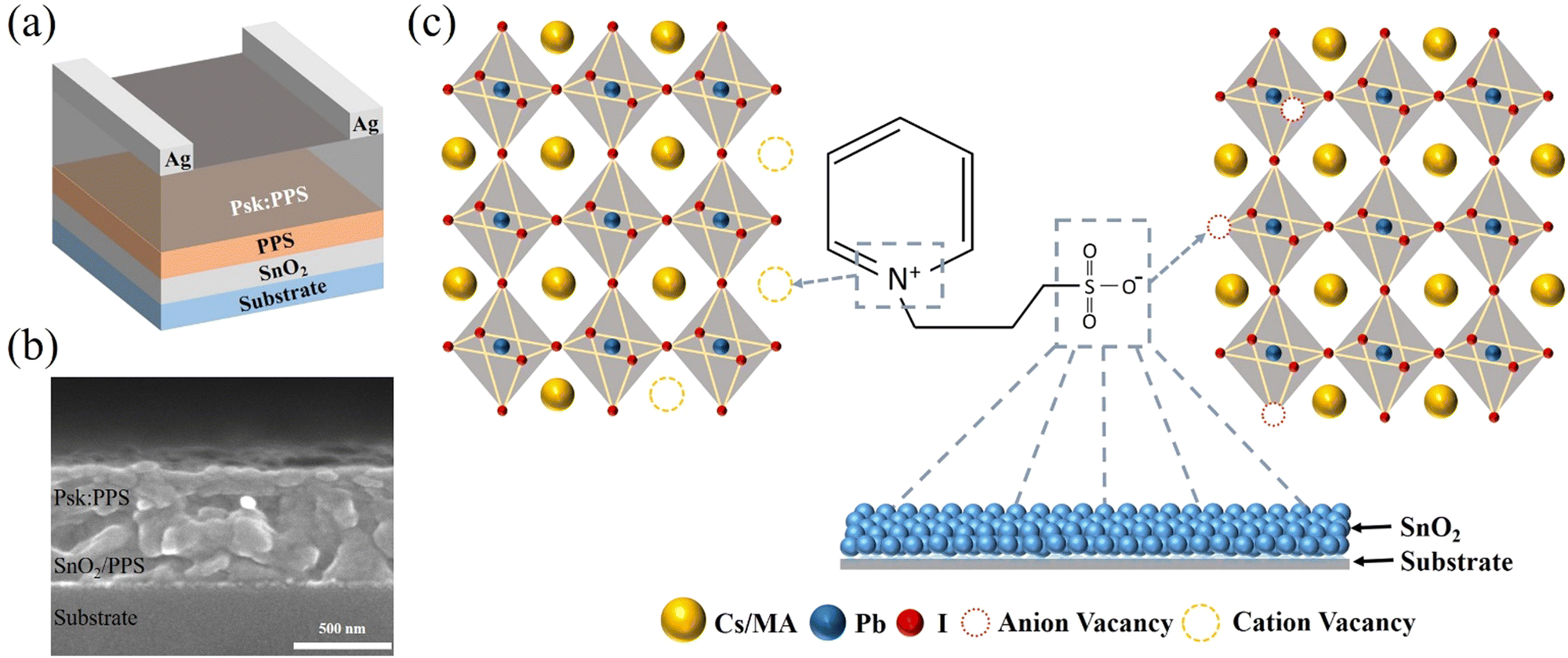 | ||
| Fig. 1 (a) Schematic representation of the device architecture of the perovskite photodetector. (b) Cross-sectional SEM image of perovskite photodetector. (c) Schematic illustration depicting the dual functionality of the PPS zwitterion. | ||
The impact of PPS on the surface morphology of perovskite films was investigated using top-view scanning electron microscopy (SEM). Fig. 2(a)–(d) illustrate the surface morphology of both the control film and the PPS treated films, while large area SEM images can be found in Fig. S4a–d, ESI.† The control film (without PPS) exhibits a significant number of pinholes and irregular grain boundaries, as depicted in Fig. 2(a). These pinholes create localized regions where charge carriers (electrons and holes) can undergo non-radiative recombination.25 Consequently, this recombination process degraded device performance by limiting the number of available carriers for detection. Incorporating 0.2 wt% PPS improves the surface morphology to some extent, although the surface remains somewhat rough, as depicted in Fig. 2(b). However, Fig. 2(c) demonstrates that an optimal amount of PPS (0.4 wt%) significantly enhances the film's surface by eliminating undesired pinholes. Incorporation of PPS additive slow down the crystallization process which improves the crystallinity of the perovskite film as shown in Fig. S5, ESI.† This results in a more uniform and denser morphology. The improved surface morphology positively impacts the photodetector device performance. Additionally, the observed reduction in grain size can be attributed to the more homogeneous growth, which can be attributed to the decreased roughness.26 On the other hand, when the PPS amount was increased to 0.6 wt%, surface irregularities and the presence of bright particles were observed. These particles are attributed to the presence of an impurity phase, as evidenced by the XRD peak at 20.94° (later shown in Fig. 3). This impurity phase leads to early charge recombination, resulting in poor photodetector device performance.
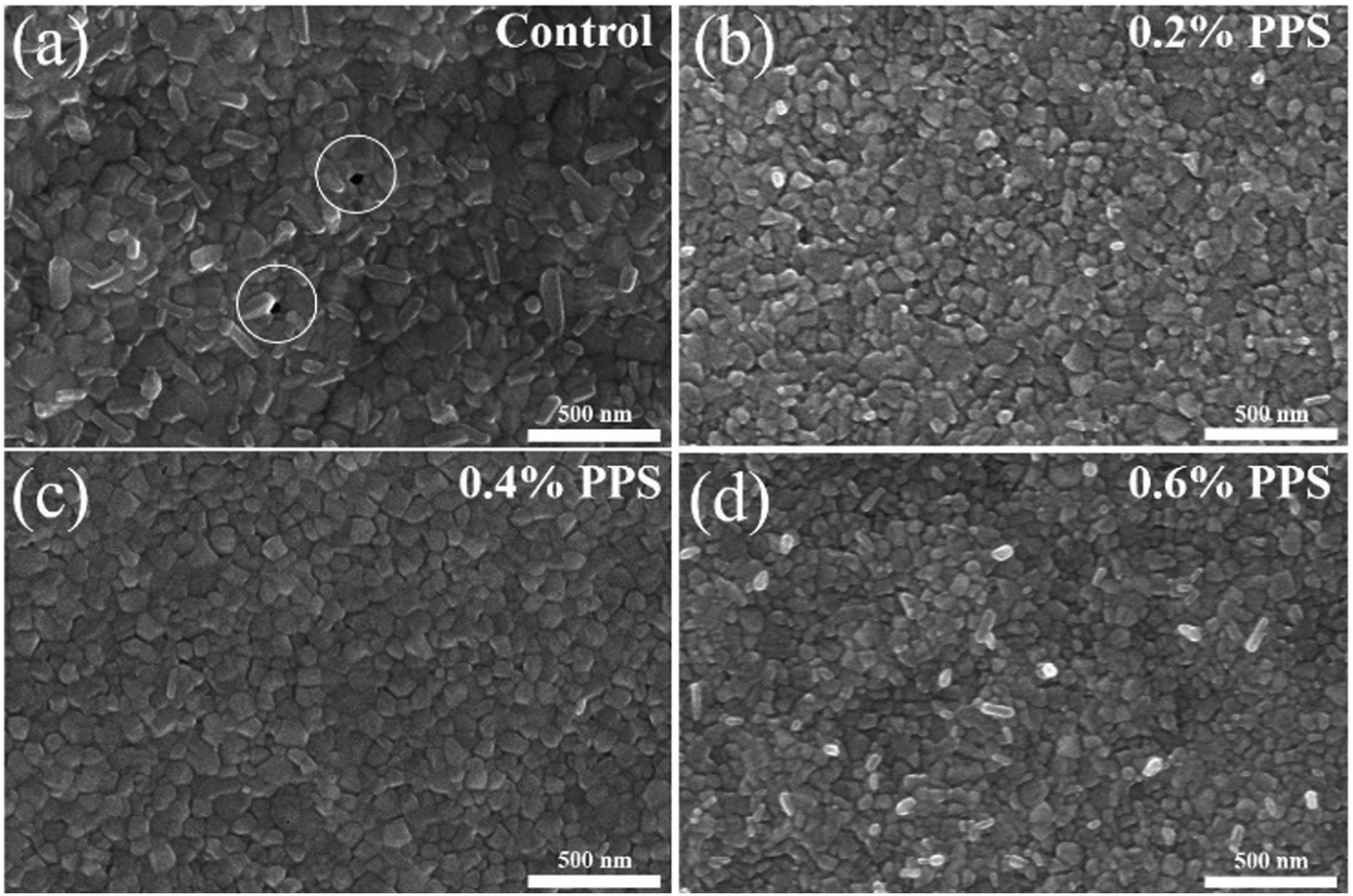 | ||
| Fig. 2 Top-view SEM images of perovskite film incorporated with (a) 0 wt%, (b) 0.2 wt%, (c) 0.4 wt%, and (d) 0.6 wt% PPS. | ||
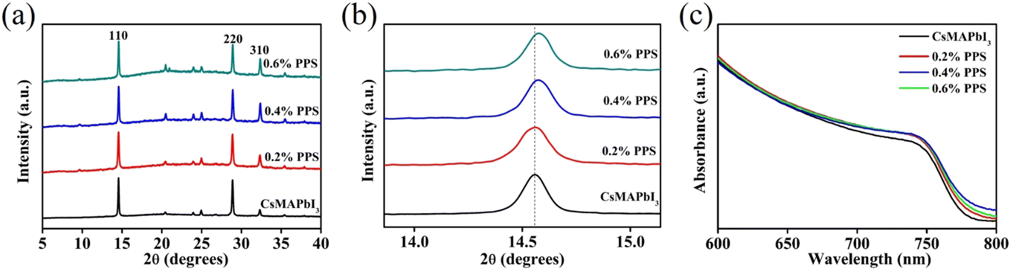 | ||
| Fig. 3 (a) X-ray diffraction (XRD) spectra and (b) zoomed-in XRD spectra of Cs0.1MA0.9PbI3 perovskite films incorporated with various PPS zwitterion concentrations. (c) UV-Vis spectra of perovskite films with various PPS zwitterion concentrations. | ||
X-ray diffraction (XRD) analyses were performed to evaluate the impact of PPS on the perovskite phase and crystallization. Fig. 3(a) represents the XRD spectra of perovskite films with varying concentrations of PPS (0 to 0.6 wt%). The characteristic peaks of the perovskite, such as (110), (220), and (310), were observed in all the samples, which indicates that the PPS incorporation does not significantly affect the crystallization. Fig. 3(b) provides a closer examination of the (110) peak. It reveals a slight blue shift from 14.54° to 14.58° when varying the PPS concentration from 0 to 0.6 wt% (the corresponding FWHM values and crystallite sizes are shown in Table S1, ESI†). This shift is attributed to the incorporation of the smaller N+ ion with a radius of 1.46 Å, as compared to Cs+ (1.81 Å) and MA+ (2.70 Å) ions, which is consistent with previous findings in the literature.27,28 The FWHM of the peaks (110), (220), and (310) can be found in Table S2, ESI.† Furthermore, the intensity of the peak (110) enhances with the incorporation of PPS (Fig. S5, ESI†). These results demonstrate the successful integration of PPS into the perovskite lattice.
UV-Vis spectroscopy was conducted to analyze the absorption spectra and bandgap (Eg) of the perovskite films with varying concentrations of PPS. Fig. 3(c) illustrates a negligible change in the absorption onset as the PPS concentration changes from 0 to 0.6 wt%. The Eg of the perovskite film changes marginally from 1.610 eV to 1.605 eV when incorporated with PPS (Corresponding Tauc plots are shown in Fig. S6, ESI†). These results show that the bandgap of the perovskite films are not significantly changed by the incorporation of PPS.29 This observation aligns with the SEM and XRD results.
The chemical compositions and electronic states of the elements contained in SnO2, SnO2/PPS, Psk, and Psk:PPS composites were investigated using XPS analysis. Fig. 4 shows the XPS spectra of SnO2 and SnO2/PPS, while those of PSK and PSK:PPS are given in Fig. 5. As can be seen, these spectra revealed the presence of key elements, i.e., C, O, Sn, Pb, and I, thus providing strong evidence for the successful preparation of the materials. Binding energy states of Pb, I, C, O, and Sn were identified by further deconvolution of these peaks. In Fig. 4(a), the survey scan spectra of SnO2 and SnO2/PPS showcased distinct peaks corresponding to the C 1s, Sn 3d, and O 1s elements at binding energies of 284, 488, and 531 eV, respectively. Fig. 4(b) illustrates the XPS spectra of Sn in 3d of SnO2, showing two distinct peaks at 487.08 and 495.48 eV for Sn 3d5/2 and Sn 3d3/2 states, respectively.30 Similarly, in SnO2/PPS, these peaks are located at 486.78 and 495.28 eV, respectively. It should be noted here that the observed bindings energies for Sn 3d5/2 and Sn 3d3/2 states in SnO2/PPS have lower values, which could be attributed to the complexation of SnO2 with PPS. The deconvoluted O 1s spectra of SnO2/PPS exhibit characteristic peaks for Sn–O and Sn–OH at 530.84 and 531.91 eV, respectively (Fig. 4(c)).31,32 The deconvoluted C 1s spectra of SnO2/PPS (Fig. 4(d)) exhibit two distinct peaks at 285.22 and 286.6 eV, attributable to CN and C–N–C chemical bonds, respectively.33 The presence of the core-level S 2p peak is clearly visible in the SnO2/PPS sample, suggesting the detection of PPS molecules on the SnO2 surface, as shown in Fig. S7a, ESI.†
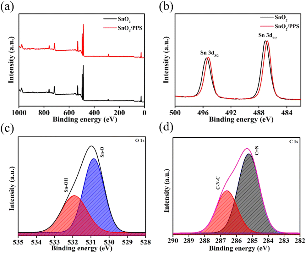 | ||
| Fig. 4 (a) Survey scan XPS spectra of SnO2 and SnO2/PPS. (b) Sn 3d XPS spectra of SnO2 and SnO2/PPS. (c) Deconvoluted O 1s and (d) deconvoluted C 1s spectra of SnO2/PPS. | ||
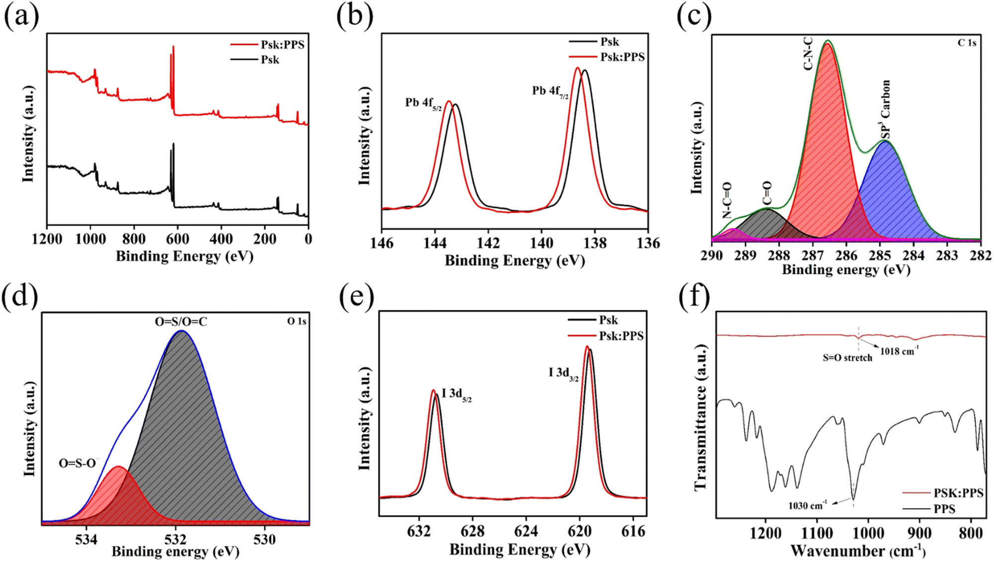 | ||
| Fig. 5 (a) Survey scan XPS spectra of Psk and Psk:PPS. (b) Pb 4f XPS spectra of Psk and Psk:PPS. (c) Deconvoluted C 1s and (d) deconvoluted O 1s spectra of Psk:PPS. (e) I 3d XPS spectra of Psk and Psk:PPS. (f) FTIR spectra of PPS and Psk:PPS. | ||
Fig. 5(a) represents the survey scan spectra of Psk and Psk:PPS composite materials, revealing characteristics peaks for Pb 4f, C 1s, O 1s, and I 3d elements at 138, 288, 531, and 619 eV, respectively. The Pb 4f spectra of Psk and Psk:PPS were deconvoluted to identify the chemical energy states of Pb in Psk and Psk:PPS materials, as shown in Fig. 5(b). The observed Pb 4f peak in both materials were found to be a combination of two peaks, namely Pb 4f7/2 and Pb 4f5/2, located at 138.38 and 143.28 eV in Psk and at 138.68 and 143.48 eV in Psk:PPS, respectively. The deconvoluted spectra of C1s in Psk are depicted in Fig. S8(a) (ESI†), displaying two distinct peaks at 284.41 and 286.63 eV. These peaks correspond to sp3 carbon and C–N–C, with peak areas measuring 676.26 and 398.19, respectively. Next, the deconvoluted C 1s spectra of PSK:PPS, as shown in Fig. 5(c), displayed characteristic pattern of four peaks at 284.83, 286.57, 288.39, and 289.37 eV.34,35 These peaks unveil the presence of sp3 carbon, C–N–C, CO, and OC–N in the sample with the peak areas values of 468.32, 791.64, 136.87, and 21.62, respectively. Notably, the reduction in the peak area of sp3 carbon contained within the PSK:PPS sample, accompanied by the emergence of CO and OC–N bonds, demonstrates the apparent impact of incorporating PPS as additive. This addition effectively stabilizes the Psk skeleton. Further, the deconvoluted spectra O 1s in Psk (Fig. S8b, ESI†) exhibited characteristic peaks for OS/OC and OS–O– at 531.85, 533.14 eV respectively, with the corresponding peak area values of 490.06 and 34.91. For Psk:PPS (Fig. 5(d)), these peaks were observed at 531.85 and 533.27 eV, and showcased peak area values of 498.79 and 74.41, respectively. The improvements in the peak areas of these dual peaks signify the formation of chemically stable compounds within the Perovskite skeleton.
Fig. 5(e) shows the deconvoluted I 3d spectra of Psk and Psk:PPS, which exhibit two distinct peaks at 619.18 and 630.68 eV corresponding to I 3d3/2 and I 3d5/2 energy states in Psk. Likewise, in Psk:PPS, these peaks are observed at 619.48 and 630.98 eV, representing the I 3d3/2 and I 3d5/2 energy states, respectively. This phenomenon contributes to the enhanced crystal symmetry of the perovskite material. In summary, the presence of PPS in Psk stabilizes its skeleton through the establishment of stable chemical bonds. This observation is further supported by the subtle shifts towards higher binding energy observed for both Pb 4f and I 3d.36 The atomic concentrations of elements are shown in Table S3 (ESI†). Overall, it can be affirmed that the obtained XPS results collectively support the conclusion of successful material preparation and highlight the influence of the complexation process. Recent studies have demonstrated that the intrinsic defects in perovskites, such as I vacancies and Pb–I antisites, can be effectively passivated using the sulfonate and pyridine ring present in PPS.23,37,38 The negatively charged oxygen atom of the sulfonate group (SO3−) forms favorable interactions with the positively charged surface of perovskites, which is induced by halide vacancies. Additionally, the interaction between Pb–I antisites and pyridine (positive charge portion) of PPS zwitterion can passivate these defects in the perovskite material. The Pb 4f peak observed in PPS incorporated perovskite exhibits a small shift to a higher binding energy compared to the control perovskite, as shown in Fig. 5(b). This shift indicates a potential chemical bond between the Pb2+ in the perovskite and the PPS zwitterion.36
The interaction between the perovskite and PPS zwitterion was further investigated using Fourier-transform infrared (FTIR) spectroscopy. Fig. 5(f) displays the absorption band of PPS at 1030 cm−1, corresponding to the SO stretching of the SO3− group in the PPS sample (complete FTIR spectra shown in Fig. S7b, ESI†). However, in the Psk:PPS sample, the absorption band shifted to 1018 cm−1, SO stretching of SO3− clearly observed in the FTIR spectra of Psk:PPS (Fig. 5(f)). This shift resulted in a formation of coordination bond between Pb2+ empty orbital of perovskite and the lone pair (SO) of PPS zwitterion. The strong interaction between PPS and the perovskite material leads to minimized surface defects, resulting in a smoother film surface as observed in Fig. 2. This smooth film surface effectively reduces undesired charge recombination, which is likely the main contributing factor to the overall performance enhancement of the photodetector device.
The optical properties, specifically the recombination of charge carriers and excitation, in the perovskite and SnO2 films were investigated using steady-state photoluminescence (PL) and time-resolved photoluminescence (TRPL) spectroscopy, as shown in Fig. 6(a) and (b). Incorporation of PPS (0.4 wt%) into the perovskite film resulted in a strong PL intensity compared to the control film (without PPS). This significant enhancement suggests a decrease in trap-assisted surface recombination within the perovskite film upon PPS incorporation.26,39 The measurements were performed with an excitation wavelength of 470 nm and 450 W Xenon Lamp as excitation source. The average thickness of the pristine and PPS incorporated perovskite films were 204 and 214 nm, respectively (Fig. S9, ESI†). The findings indicate that incorporation of PPS (0.4 wt%) significantly suppressed the recombination in perovskite film. Consequently, the addition of PPS (0.4 wt%) enhances charge carrier transfer and reduces non-radiative recombination defects. Furthermore, the PPS incorporated perovskite sample exhibits a blue shift, indicating a lower trap density near the band-edge of the perovskite film.40,41 Fig. S10a, ESI,† shows the PL spectra of SnO2/Psk:PPS and SnO2/PPS(0.2 wt%)/Psk:PPS samples. The photoluminescence (PL) quenching observed in the SnO2/PPS(0.2 wt%)/Psk:PPS sample indicates the enhanced charge extraction ability of the SnO2 layer treated with PPS, as compared to the bare SnO2 layer. This improvement suggests that the transfer of electrons from active layer to SnO2/PPS layer.
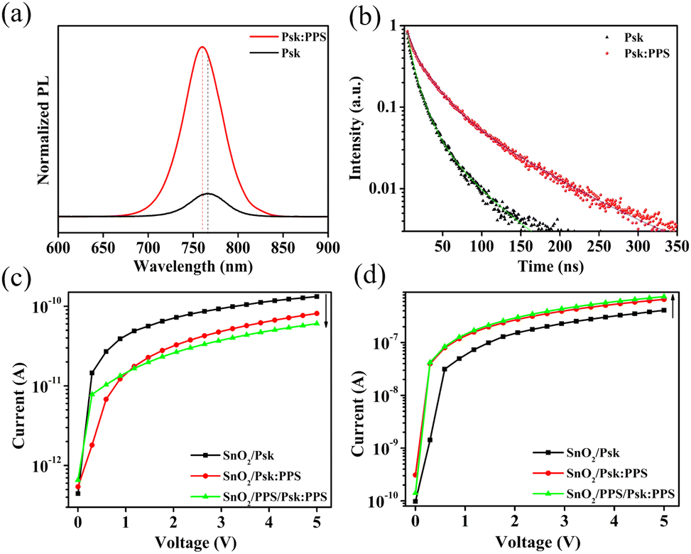 | ||
| Fig. 6 (a) Normalized steady-state photoluminescence spectra with respect to optical density and (b) time-resolved photoluminescence spectra of perovskite film with/without PPS zwitterion. I–V characteristics of SnO2/Psk, SnO2/Psk:PPS, and SnO2/PPS/Psk:PPS devices under (c) dark and (d) illuminated conditions. | ||
Furthermore, the carrier lifetime was evaluated using time-resolved photoluminescence (TRPL) spectra (Fig. 6(b)), revealing that the perovskite film treated with PPS additive (0.4 wt% PPS) exhibits a longer charge carrier lifetime in contrast with the perovskite film without PPS. The average charge carrier lifetimes measured were 51.35 ns for the PPS incorporated perovskite film and 10 ns for the perovskite film without PPS (see Table S4, ESI,† for detailed parameters). This longer lifetime suggests a reduction in non-radiative charge carrier recombination and a lower defect density in the PPS incorporated perovskite film, leading to a stronger photoluminescence (PL) intensity in the spectrum. This longer charge carrier lifetime can be attributed to a decrease in the trap-state density at the grain boundaries and surface, which is consistent with our observations from the SEM results in Fig. 2. The TRPL spectra of the complete devices are shown in Fig. S10b, ESI,† which further confirm these findings. In addition, the average PL lifetime significantly decreases for the SnO2/PPS(0.2 wt%)/Psk:PPS devices compared to the SnO2/Psk:PPS devices (see Table S5, ESI,† for detailed parameters). This decrease indicates a significant improvement in the electron extraction ability of the SnO2 layer upon treatment with PPS.
Fig. 6(c) and (d) display the current–voltage (I–V) curves of the photodetector devices under light power intensity of 1 mW cm−2. The device structures are SnO2/Psk, SnO2/Psk:PPS, and SnO2/PPS/Psk:PPS. Fig. 6(c) shows the dark current characteristics of these devices. SnO2/Psk exhibits the highest dark current of 1.32 × 10⁻¹⁰ A, while SnO2/Psk:PPS shows a lower dark current of 8.12 × 10⁻¹¹ A after incorporating 0.4 wt% PPS into the perovskite. Notably, SnO2/PPS/Psk:PPS demonstrates the lowest dark current of 6.05× 10⁻¹¹ A, achieved by introducing a PPS (0.2 wt%) interlayer onto the SnO2 layer and incorporating PPS (0.4 wt%) into the perovskite. This dark current reduction can be attributed to multiple factors: (i) the incorporation of PPS (0.4 wt%) into the perovskite, which reduces defects in the film, and (ii) the introduction of a PPS (0.2 wt%) interlayer onto the SnO2 layer, which improves the interface between the layers.
The SnO2/Psk:PPS device shows lower dark current compared to SnO2/Psk device due to the incorporation of PPS (0.4 wt%) into the perovskite. This incorporation effectively reduces cation and anion vacancies in the perovskite film, which leads to a reduction in film defects. These defects (Pb2+ and Pb–I antisites) are an important cause of the dark current.42–44 Consequently, the decrease in these defects improves the surface quality of the film, as demonstrated in Fig. 2, resulting in a decrease in dark current generation. The photodetector device shows further decrease in dark current by introducing a PPS (0.2 wt%) interlayer onto the SnO2 layer (SnO2/PPS/Psk:PPS < SnO2/Psk:PPS). This interlayer reduces oxygen vacancies in the SnO2 film (as shown in Fig. 4) and improves the interface between SnO2 and the perovskite.23 This improved interface narrows the conducting regions between the two films, resulting in a decrease in the dark current.45 Dark currents of photodetector devices with different additive concentrations of PPS in the perovskite are shown in Fig. S11a and c, ESI,† while photodetector devices with different interlayer concentration of PPS on SnO2 are shown in Fig. S12a, ESI.†
Fig. 6(d) illustrates the photocurrent characteristics of the photodetector devices. Among them, the SnO2/PPS/Psk:PPS device exhibits a highest photocurrent (7.41 × 10⁻⁷ A) than the SnO2/Psk (4.08 × 10⁻⁷ A) and SnO2/Psk:PPS (6.58× 10⁻⁷ A) devices. Firstly, the photocurrent of the SnO2/Psk:PPS device is enhanced due to the incorporation of PPS (0.4 wt%) into the perovskite. This incorporation of zwitterion into perovskite improves the surface morphology (as shown in Fig. 2), leading to a decrease in recombination of charge carriers and an increase in the PL lifetime. Consequently, the photocurrent of the SnO2/Psk:PPS device is enhanced compared to the SnO2/Psk device. Secondly, the SnO2/PPS/Psk:PPS device exhibits an even higher photocurrent compared to the SnO2/Psk:PPS device, which is attributed to the addition of a PPS (0.2 wt%) interlayer onto the SnO2 layer. This enhanced photocurrent is a result of the improved interface between SnO2/PPS and the perovskite, as previously shown in Fig. 1(b). This improved interface enhances extraction of charges from the active perovskite layer to the SnO2/PPS layer. Consequently, when light falls on the absorber layer, electron–hole pairs are generated and separated at the formed heterojunction. The addition of the PPS interlayer enhances the extraction and transportation of electrons in the SnO2 layer. The electrons are efficiently transported to the SnO2/PPS layer, while the holes remain in the perovskite layer.46 This enhanced charge separation reduces early charge carrier recombination, resulting in an increased photocurrent. Consequently, the SnO2/PPS/Psk:PPS device exhibits the highest photocurrent than the SnO2/Psk and SnO2/Psk:PPS devices. The photocurrents of photodetector devices with different concentrations of PPS in the perovskite are shown in Fig. S11b and d, ESI,† while the photocurrents of photodetector devices with varying interlayer concentrations of PPS on SnO2 are demonstrated in Fig. S12b, ESI.† All the calculated I–V characteristics can be found in Tables S6–S9, ESI.†
The light to dark current ratio (ILight/Idark) is an important factor to consider when characterizing photodetectors. ILight/Idark values for all the devices were calculated at a 5 V bias and under light intensity of 1 mW cm−2. The calculated ILight/Idark values for SnO2/Psk, SnO2/Psk:PPS, and SnO2/PPS/Psk:PPS devices are 3.1 × 10³, 8.1 × 10³, and 1.2 × 10⁴, respectively, as shown in Table S6 (ESI†). These values indicate the amplification of light signals compared to the dark current levels. ILight/Idark values for different concentrations of PPS in the perovskite and different concentrations of PPS on SnO2 can be found in Tables S7–S9 (ESI†).
Responsivity (R) is a fundamental parameter used to evaluate the sensitivity of a photodetector to light illumination, as shown in eqn (1):
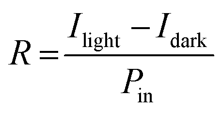 | (1) |
In eqn (1), Ilight refers to the current measured under light conditions, Idark refers to the current measured under dark conditions, and Pin represents the power of the light falling on the active area.46,47Eqn (1) demonstrates that the responsivity can be enhanced by increasing the applied voltage, decreasing the light power, and reducing the length of the channel. At an illumination power of 1 mW cm−2, the responsivity values for SnO2/Psk, SnO2/Psk:PPS, and SnO2/PPS/Psk:PPS devices are 3.26 A W−1, 5.27 A W−1, and 5.93 A W−1, respectively. The higher responsivity of SnO2/PPS/Psk:PPS can be attributed to its lower dark current and higher photocurrent. Tables S7–S9, ESI,† present the responsivity values of the photodetector devices with different concentrations of PPS used as both an additive and an interlayer material.
Detectivity (D*) is a vital factor employed to assess the light detection ability of PD.45 It can be calculated by the following equation:
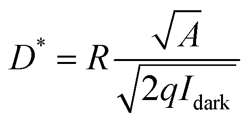 | (2) |
In eqn (2), A represents the active area of the device and q is the electron charge (1.6 × 10⁻¹⁹ C). The detectivity values of SnO2/Psk, SnO2/Psk:PPS, and SnO2/PPS/Psk:PPS devices are 5.62 × 10⁻¹² J, 1.15 × 10¹³ J, and 1.51 × 10¹³ J, respectively. Tables S7–S9, ESI,† present the detectivity values of the devices with different concentrations of PPS used as both an additive and an interlayer material.
Fig. 7 illustrates the on–off switching behavior of the SnO2/Psk, SnO2/Psk:PPS, and SnO2/PPS/Psk:PPS photodetector devices. These characteristics were measured under a 2 V bias and white light illumination of 1 mW cm−2. Fig. 7(a)–(c) display repetitive cycles of the SnO2/Psk, SnO2/Psk:PPS, and SnO2/PPS/Psk:PPS devices. During light illumination, the current rapidly increases and reaches its peak in all of the photodetector devices; it then remains stable until the illumination is turned off.
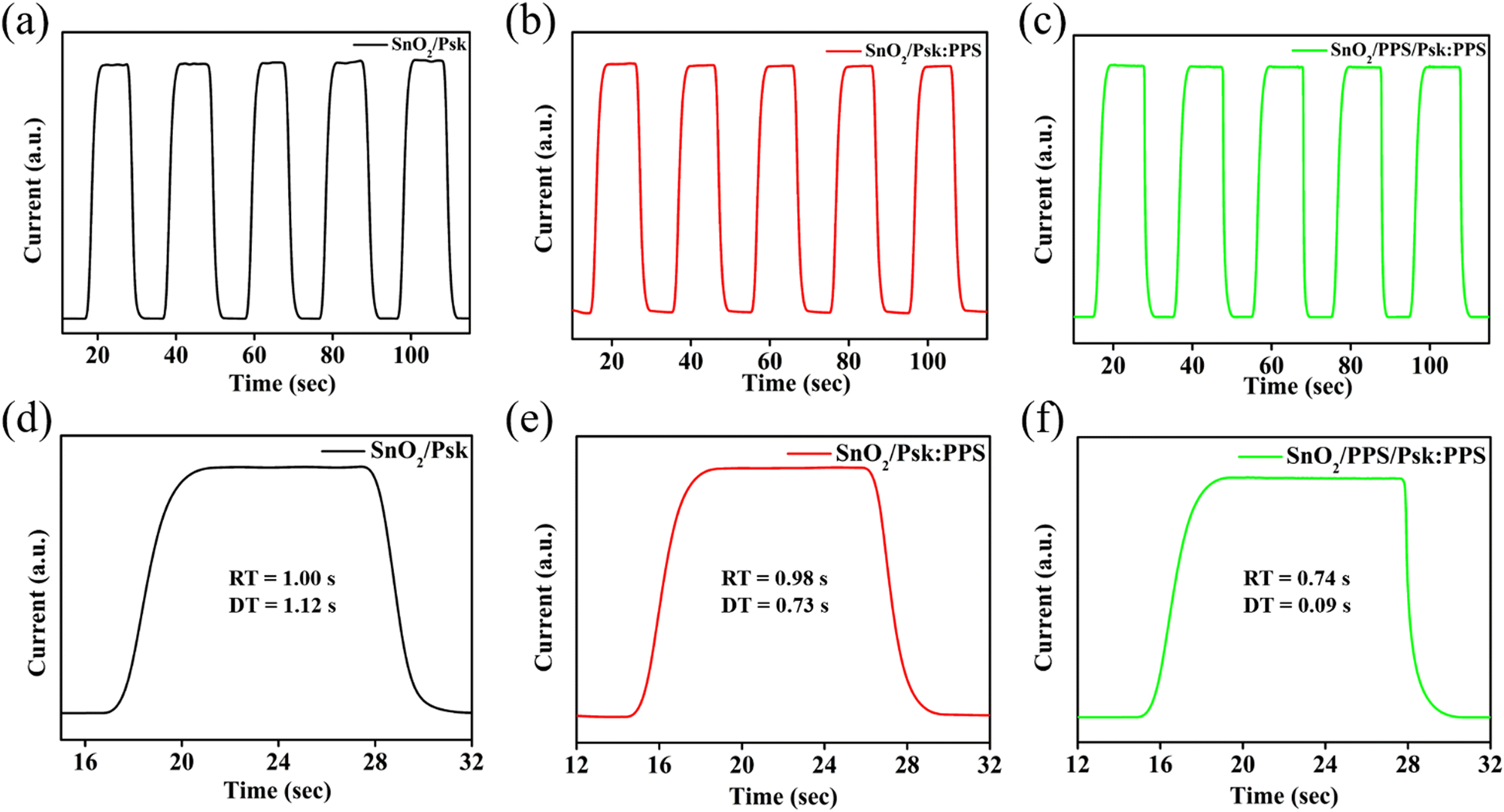 | ||
| Fig. 7 Switching characteristics of (a) SnO2/Psk, (b) SnO2/Psk:PPS, and (c) SnO2/PPS/Psk:PPS devices. Single cycle rise and decay for (d) SnO2/Psk, (e) SnO2/Psk:PPS, and (f) SnO2/PPS/Psk:PPS devices. | ||
Fig. 7(d)–(f) illustrate the single on–off cycle characteristics of SnO2/Psk, SnO2/Psk:PPS, and SnO2/PPS/Psk:PPS photodetector devices. The calculated rise and decay times for SnO2/Psk are 1.00 s and 1.12 s, respectively. For SnO2/Psk:PPS, the rise time is 0.98 s and the decay time is 0.73 s. Finally, SnO2/PPS/Psk:PPS exhibits a rise time of 0.74 s and a decay time of 0.09 s (shown in Table S6, ESI†). The rise and decay time are limited by the resolution of the Keithley source meter.48 However, SnO2/PPS/Psk:PPS device demonstrates the shortest rise and decay times among the photodetector devices, confirming the consistency with the results obtained from the I–V measurements.
The signal-to-noise ratio (SNR) is an essential parameter for characterizing photodetector devices. SNR is a measure of the strength of a signal relative to the background noise:45
 | (3) |
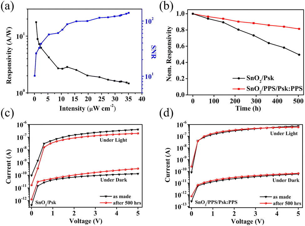
The SNR values for SnO2/Psk, SnO2/Psk:PPS, and SnO2/PPS/Psk:PPS are calculated to be 3.1 × 10³, 8.1 × 10³, and 1.2 × 10⁴, respectively. Fig. 8(a) illustrates the impact of varying the light illumination intensity on the R and SNR of the photodetector devices. These results demonstrate that increasing the illumination intensity leads to a decrease in responsivity and an increase in SNR. Increasing light intensity decreases device responsivity and increases SNR. This is because a higher illumination intensity results in the generation of more photogenerated charge carriers, leading to a larger photocurrent; this increased photocurrent contributes to an enhanced SNR. Increasing the illumination intensity leads to a reduction in the available number of photogenerated carriers for extraction. This can be attributed to the saturation of recombination and trap states, which affects the carriers lifetime. Consequently, the responsivity decreases.49
 | ||
| Fig. 8 (a) Responsivity and signal-to-noise ratio (SNR) of the SnO2/PPS/Psk:PPS photodetector device. (b) Environmental stability of unencapsulated SnO2/Psk and SnO2/PPS/Psk:PPS devices under ambient conditions at room temperature and 40–50% humidity. 500 hour I–V stability of unencapsulated (c) SnO2/Psk and (d) SnO2/PPS/Psk:PPS devices. | ||
Finally, the photodetector devices underwent a current–voltage (I–V) stability test, as shown in Fig. 8(b)–(d). The samples were placed in an ambient environment at room temperature with a humidity level of approximately 40–50% for 500 hours. (See Fig. S13 for sample images and Fig. S14 for thermal stability images in the ESI†). After the stability test, the SnO2/PPS/Psk:PPS device retained approximately 80% of its original responsivity, while the SnO2/Psk photodetector device only retained 50% of its initial responsivity. The poor stability observed in the SnO2/Psk device can be attributed to trap-assisted non-radiative recombination originating from irregular surfaces and pinholes, which significantly degraded the overall device performance.50,51Fig. 8(c) and (d) illustrates the I–V results of SnO2/Psk and SnO2/PPS/Psk:PPS devices, respectively. These results demonstrate a notable increase in the dark current of the SnO2/Psk device after 500 hours; this is in contrast to the SnO2/PPS/Psk:PPS device, which exhibits a more stable dark current over the same period. Furthermore, the SnO2/Psk device exhibits a lower photocurrent compared to the SnO2/PPS/Psk:PPS device. Two important factors are responsible for the enhanced stability of the SnO2/PPS/Psk:PPS device: (i) the enhanced surface morphology and reduction in defects resulting from the strong interaction between the PPS and perovskite, as evidenced by the XPS results shown in Fig. 5, and (ii) the incorporation of a PPS interlayer, which improves the interface between the SnO2 and perovskite. These improvements contribute to the improved stability observed in the SnO2/PPS/Psk:PPS device.
Conclusions
In this study, we have successfully developed a method to simultaneously modify the perovskite and SnO2 electron transport layer through additive and interface engineering. By incorporating a bifunctional zwitterion PPS into the perovskite film, we were able to passivate both negatively and positively charged defects within the perovskite film. XPS and FTIR analyses confirmed the strong interaction between the PPS zwitterion and the perovskite material. Additionally, we deposited PPS as an interlayer between SnO2 and the perovskite, resulting in an improved interface and enhanced charge extraction from the perovskite layer. The incorporation of PPS and the addition of the PPS interlayer significantly improved the performance and stability of the photodetector device. The device exhibited a low dark current of 6.05 × 10⁻¹¹ A, an excellent responsivity of 5.93 A W−1, a detectivity of 1.51 × 10¹³ J, and an on/off ratio of 1.2 × 10⁴. Moreover, the photodetector device demonstrated exceptional stability, retaining 80% of its original responsivity under ambient conditions after 500 hours. Overall, our findings provide an effective strategy for the perovskite research community to achieve high-performance and stable photodetector devices.Experimental section
Material preparation
We obtained MAI, CsI, PbI2, DMSO, and PPS from Aldrich; DMF from Fujifilm Wako Pure Chemical Company; methanol from DaeJung; CB from TCI; and SnO2 (15% in a water colloidal dispersion) from Alfa Aesar. None of these materials underwent any further purification before use.Initially, a 1 M Cs0.1MA0.9PbI3 precursor solution was prepared. This was accomplished by dissolving CsI, MAI, and PbI2 (at a ratio of 0.1![[thin space (1/6-em)]](https://www.rsc.org/images/entities/char_2009.gif) :0.9:1) in DMF and DMSO (at a ratio of 1:4). PPS was then added to the precursor solution in amounts ranging from 0 to 0.6 wt%, and the solution was stirred at 60 °C overnight. In addition, a compact SnO2 colloid precursor solution was prepared by mixing stannic oxide and ultrapure water at a volume ratio of 1:6, and stirred at room temperature for 30 minutes. To prepare the PPS solution, different concentrations of PPS ranging from 0 to 0.4 wt% were added to methanol and stirred at 45 °C for 4 hours.
:0.9:1) in DMF and DMSO (at a ratio of 1:4). PPS was then added to the precursor solution in amounts ranging from 0 to 0.6 wt%, and the solution was stirred at 60 °C overnight. In addition, a compact SnO2 colloid precursor solution was prepared by mixing stannic oxide and ultrapure water at a volume ratio of 1:6, and stirred at room temperature for 30 minutes. To prepare the PPS solution, different concentrations of PPS ranging from 0 to 0.4 wt% were added to methanol and stirred at 45 °C for 4 hours.
Device fabrication
The sapphire-coated glass substrates were subjected to ultrasonic cleaning using a detergent, deionized water, acetone, and IPA, with each cleaning step lasting 20 minutes. Hereafter, the substrates were further cleaned by plasma for 15 minutes to eliminate any remaining particles. Next, the SnO2 colloid was deposited at a rate of 3000 rpm for 45 s, and annealed at 150 °C for 30 minutes. For the SnO2/PPS sample, the PPS solution (with a concentration of 0 to 0.4 wt% in methanol) was spin coated on the SnO2 layer at 4000 rpm for 30 s. The sample was then annealed at 100 °C for 10 minutes. Following that, a perovskite precursor solution incorporated with PPS molecules was deposited above the SnO2/PPS layer using a two-step spin-coating technique. The first step involved spinning the substrate at 1000 rpm for 10 s, followed by a second spin-coating step at 5000 rpm for 30 s. During the second step, CB was poured as anti-solvent at suitable interval of time. Lastly, silver (Ag) electrodes were deposited via thermal evaporation in a high-vacuum environment (10−6 Pa). All the experiments were performed in an ambient (open-air) environment.Characterization
The current–voltage (I–V) values were measured by using a Keithley 2635b instrument under a customized probe station in a dark shield box (MSD2). The photoluminescence spectra were measured by an iHR320 spectrometer with 450 W Xenon lamp as excitation source, and the integration time was set to 0.1 seconds, and data was collected with an increment of 1.00 nm. The time-resolved PL spectra were measured by a FlouTime 300 spectrometer. The top-view morphological scans of the samples were collected with an FESEM Apreo SHivac instrument. XRD patterns were acquired by using a MINI XRD instrument (miniFlex600). XPS peaks were deconvoluted with Origin 8.5 software. The UV-Vis spectra of the samples were collected and analyzed by a Lambda 650S instrument. MultiLab ESCA 2000 device was used to obtain the XPS spectra of materials. Thermo Nicolet iS50 spectrometer (range 3500–500 cm−1) was used to observe FTIR spectra.Author contributions
Conceptualization: A. A. Khan, N. Kumar, and J. Park. Formal analysis: A. A. Khan and N. Kumar. Funding acquisition: J. Park. Investigation: A. A. Khan, N. Kumar, U. Jung, W. Heo, and Z. Tan. Methodology: A. A. Khan and N. Kumar. Supervision: J. Park. Writing – original draft: A. A. Khan and N. Kumar. Writing – review & editing: All authors.Conflicts of interest
There are no conflicts of interest to declare.Acknowledgements
This research work was supported by the National Research Foundation of Korea (NRF), funded by the Korean government (MSIT) (no. 2021R1A4A1052085).References
- C.-Y. Chang, K.-S. Wu and C.-Y. Chang, Adv. Funct. Mater., 2022, 32, 2108356 CrossRef CAS.
- A. J. J. M. van Breemen, R. Ollearo, S. Shanmugam, B. Peeters, L. C. J. M. Peters, R. L. van de Ketterij, I. Katsouras, H. B. Akkerman, C. H. Frijters, F. Di Giacomo, S. Veenstra, R. Andriessen, R. A. J. Janssen, E. A. Meulenkamp and G. H. Gelinck, Nat. Electron., 2021, 4, 818–826 CrossRef CAS.
- Y. Yue, M. Li, H. Li, N. Chai, Y. Dong, Z. Li, X. Chen and X. Wang, Chem. Eng. J., 2022, 441, 135997 CrossRef CAS.
- M. Azam, A. A. Khan, G.-X. Liang, G.-J. Li, S. Chen, Z.-H. Zheng, U. Farooq, M. Ishaq, P. Fan, Z. Wang and Z.-G. Wang, Sol. RRL, 2020, 4, 2000358 CrossRef CAS.
- A. Kojima, K. Teshima, Y. Shirai and T. Miyasaka, J. Am. Chem. Soc., 2009, 131, 6050–6051 CrossRef CAS PubMed.
- S. You, F. T. Eickemeyer, J. Gao, J.-H. Yum, X. Zheng, D. Ren, M. Xia, R. Guo, Y. Rong, S. M. Zakeeruddin, K. Sivula, J. Tang, Z. Shen, X. Li and M. Grätzel, Nat. Energy, 2023, 8, 515–525 CrossRef CAS.
- S.-Q. Sun, Q. Sun, Y.-J. Ji, Y.-L. Xu, W. He, M. Zhu, J.-G. Zhou, Y.-J. Yu, D.-D. Feng, Y.-M. Xie, Y.-Y. Li and M.-K. Fung, Small, 2023, 19, 2205336 CrossRef CAS PubMed.
- C. Kuang, Z. Hu, Z. Yuan, K. Wen, J. Qing, L. Kobera, S. Abbrent, J. Brus, C. Yin, H. Wang, W. Xu, J. Wang, S. Bai and F. Gao, Joule, 2021, 5, 618–630 CrossRef CAS.
- A. Hassan, M. Azam, Y. H. Ahn, M. Zubair, Y. Cao and A. A. Khan, Nanomaterials, 2022, 12(2), 190 CrossRef CAS PubMed.
- W. Shen, U. Jung, Z. Xian, B. Jung and J. Park, J. Alloys Compd., 2022, 929, 167329 CrossRef CAS.
- Y. Wang, X. Cao, G. Niu, Y. Dong, Z. Yang, Y. Liu, J. Wang and S. Cao, J. Alloys Compd., 2023, 939, 168712 CrossRef CAS.
- J. Zhuang, P. Mao, Y. Luan, X. Yi, Z. Tu, Y. Zhang, Y. Yi, Y. Wei, N. Chen, T. Lin, F. Wang, C. Li and J. Wang, ACS Energy Lett., 2019, 4, 2913–2921 CrossRef CAS.
- L. Fu, H. Li, L. Wang, R. Yin, B. Li and L. Yin, Energy Environ. Sci., 2020, 13, 4017–4056 RSC.
- M. Azam, S. Yue, R. Xu, K. Liu, K. Ren, Y. Sun, J. Liu, Z. Wang, S. Qu, Y. Lei and Z. Wang, J. Mater. Chem. A, 2018, 6, 13725–13734 RSC.
- T.-H. Han, J.-W. Lee, C. Choi, S. Tan, C. Lee, Y. Zhao, Z. Dai, N. De Marco, S.-J. Lee, S.-H. Bae, Y. Yuan, H. M. Lee, Y. Huang and Y. Yang, Nat. Commun., 2019, 10, 520 CrossRef CAS PubMed.
- J. Chen, S.-G. Kim, X. Ren, H. S. Jung and N.-G. Park, J. Mater. Chem. A, 2019, 7, 4977–4987 RSC.
- N. Ma, J. Jiang, Y. Zhao, L. He, Y. Ma, H. Wang, L. Zhang, C. Shan, L. Shen and W. Hu, Nano Energy, 2021, 86, 106113 CrossRef CAS.
- A. A. Khan, M. Azam, D. Eric, G. Liang and Z. Yu, J. Mater. Chem. C, 2020, 8, 2880–2887 RSC.
- Y. Wang, G. Niu, X. Cao, Z. Yang, Y. Dong, G. Feng, Y. Liu, J. Wang and S. Cao, Chem. Eng. J., 2023, 459, 141602 CrossRef CAS.
- S. Jiang, Z. Hou, X. Zheng, Q. Wu, X. Yang, W. Cai, Y. Yi, S. Cheng, G. Wen and X. Liu, J. Mater. Chem. C, 2023, 11, 5667–5679 RSC.
- A. A. Khan, Z. Yu, U. Khan and L. Dong, Nanoscale Res. Lett., 2018, 13, 399 CrossRef PubMed.
- X. Zhang, X. Liu, B. Sun, Z. Liu, Z. Zhang, L. Kong, G. Li, M. Wang, Z. Liu and G. Liao, J. Mater. Chem. C, 2022, 10, 14892–14904 RSC.
- K. Choi, J. Lee, H. I. Kim, C. W. Park, G.-W. Kim, H. Choi, S. Park, S. A. Park and T. Park, Energy Environ. Sci., 2018, 11, 3238–3247 RSC.
- D. Zheng, R. Peng, G. Wang, J. L. Logsdon, B. Wang, X. Hu, Y. Chen, V. P. Dravid, M. R. Wasielewski, J. Yu, W. Huang, Z. Ge, T. J. Marks and A. Facchetti, Adv. Mater., 2019, 31, 1903239 CrossRef CAS PubMed.
- T. P. Baumeler, E. A. Alharbi, G. Kakavelakis, G. C. Fish, M. T. Aldosari, M. S. Albishi, L. Pfeifer, B. I. Carlsen, J.-H. Yum, A. S. Alharbi, M. D. Mensi, J. Gao, F. T. Eickemeyer, K. Sivula, J.-E. Moser, S. M. Zakeeruddin and M. Grätzel, ACS Energy Lett., 2023, 8, 2456–2462 CrossRef CAS.
- N. Li, J. Liu, C. Li, Y. Li, J. Jia, Y. Wu, H. Yu, B. Yuan and B. Cao, ACS Sustainable Chem. Eng., 2020, 8, 7020–7030 CrossRef CAS.
- X. Zhu, D. Yang, R. Yang, B. Yang, Z. Yang, X. Ren, J. Zhang, J. Niu, J. Feng and S. Liu, Nanoscale, 2017, 9, 12316–12323 RSC.
- M. Saliba, T. Matsui, J.-Y. Seo, K. Domanski, J.-P. Correa-Baena, M. K. Nazeeruddin, S. M. Zakeeruddin, W. Tress, A. Abate, A. Hagfeldt and M. Grätzel, Energy Environ. Sci., 2016, 9, 1989–1997 RSC.
- Y. Ji, J.-B. Zhang, H.-R. Shen, Z. Su, H. Cui, T. Lan, J.-Q. Wang, Y.-H. Chen, L. Liu, K. Cao, W. Shen and S. Chen, ACS Omega, 2021, 6, 13831–13838 CrossRef CAS PubMed.
- J. S. Kim, N. Kumar, U. Jung, J. Park and M. Naushad, Chemosphere, 2023, 331, 138780 CrossRef CAS PubMed.
- M. Kwoka, B. Lyson-Sypien, E. Comini, M. Krzywiecki, K. Waczynski and J. Szuber, Nanotechnology, 2020, 31, 315714 CrossRef CAS PubMed.
- V. Bonu, A. Das, M. Sardar, S. Dhara and A. K. Tyagi, J. Mater. Chem. C, 2015, 3, 1261–1267 RSC.
- S. Lyu, Y. Chen, S. Han, L. Guo, Z. Chen, Y. Lu, Y. Chen, N. Yang and S. Wang, RSC Adv., 2018, 8, 13191–13199 RSC.
- S. Verma, K.-H. Kim, N. Kumar, S. S. Bhattacharya, M. Naushad and R. K. Dutta, J. Hazard. Mater., 2022, 429, 128308 CrossRef CAS PubMed.
- N. Kumar and V. C. Srivastava, Renewable Energy, 2021, 175, 1–13 CrossRef CAS.
- Q. Zhou, J. Qiu, Y. Wang, M. Yu, J. Liu and X. Zhang, ACS Energy Lett., 2021, 6, 1596–1606 CrossRef CAS.
- Y. Zhao, P. Zhu, S. Huang, S. Tan, M. Wang, R. Wang, J. Xue, T.-H. Han, S.-J. Lee, A. Zhang, T. Huang, P. Cheng, D. Meng, J.-W. Lee, J. Marian, J. Zhu and Y. Yang, J. Am. Chem. Soc., 2020, 142, 20071–20079 CrossRef CAS PubMed.
- X. Zheng, Y. Deng, B. Chen, H. Wei, X. Xiao, Y. Fang, Y. Lin, Z. Yu, Y. Liu, Q. Wang and J. Huang, Adv. Mater., 2018, 30, 1803428 CrossRef PubMed.
- X. Li, D. Bi, C. Yi, J.-D. Décoppet, J. Luo, S. M. Zakeeruddin, A. Hagfeldt and M. Grätzel, Science, 2016, 353, 58–62 CrossRef CAS PubMed.
- S. Yuan, F. Qian, S. Yang, Y. Cai, Q. Wang, J. Sun, Z. Liu and S. Liu, Adv. Funct. Mater., 2019, 29, 1807850 CrossRef CAS.
- D. Wei, F. Ma, R. Wang, S. Dou, P. Cui, H. Huang, J. Ji, E. Jia, X. Jia, S. Sajid, A. M. Elseman, L. Chu, Y. Li, B. Jiang, J. Qiao, Y. Yuan and M. Li, Adv. Mater., 2018, 30, 1707583 CrossRef PubMed.
- D. McGrath, S. Tobin, V. Goiffon, P. Magnan and A. Le Roch, Electron. Imaging, 2018, 30, 354-1–354-8 CrossRef.
- B. W. Hendrickson, DC-RTS Noise: Observation and Analysis, Portland State University, 2019 DOI:10.15760/etd.7241.
- Z. Jin and J. Wang, J. Mater. Chem. C, 2014, 2, 1966–1970 RSC.
- Z. Ren, J. Sun, H. Li, P. Mao, Y. Wei, X. Zhong, J. Hu, S. Yang and J. Wang, Adv. Mater., 2017, 29, 1702055 CrossRef PubMed.
- X. Yi, Z. Ren, N. Chen, C. Li, X. Zhong, S. Yang and J. Wang, Adv. Electron. Mater., 2017, 3, 1700251 CrossRef.
- Y. Wei, G. Feng, P. Mao, Y. Luan, J. Zhuang, N. Chen, H. Yang, W. Li, S. Yang and J. Wang, ACS Appl. Mater. Interfaces, 2020, 12, 8826–8834 CrossRef CAS PubMed.
- S. Cheng, X. Zheng, Z. Hou, R. Hu, S. Jiang, S. Xi, G. Wen and X. Liu, J. Mater. Chem. C, 2022, 10, 5693–5706 RSC.
- R. Zhuo, S. Zuo, W. Quan, D. Yan, B. Geng, J. Wang and X. Men, RSC Adv., 2018, 8, 761–766 RSC.
- N. Ahn, K. Kwak, M. S. Jang, H. Yoon, B. Y. Lee, J.-K. Lee, P. V. Pikhitsa, J. Byun and M. Choi, Nat. Commun., 2016, 7, 13422 CrossRef CAS PubMed.
- J. Chen and N.-G. Park, Adv. Mater., 2019, 31, 1803019 CrossRef CAS PubMed.
Footnote |
| † Electronic supplementary information (ESI) available. See DOI: https://doi.org/10.1039/d3nh00263b |
| This journal is © The Royal Society of Chemistry 2023 |