
Localized coherent phonon generation in monolayer MoSe2 from ultrafast exciton trapping at shallow traps†
Soungmin
Bae‡
ab,
Tae Young
Jeong‡
c,
Hannes
Raebiger
b,
Ki-Ju
Yee
*c and
Yong-Hoon
Kim
 *a
*a
aDepartment of Electrical Engineering, Korea Advanced Institute of Science and Technology (KAIST), Daejeon 34141, Korea. E-mail: y.h.kim@kaist.ac.kr
bDepartment of Physics, Yokohama National University, Yokohama, Japan
cDepartment of Physics, Chungnam National University, Daejeon 34134, Korea. E-mail: kyee@cnu.ac.kr
First published on 11th July 2023
Abstract
We report spectroscopic evidence for the ultrafast trapping of band edge excitons at defects and the subsequent generation of defect-localized coherent phonons (CPs) in monolayer MoSe2. While the photoluminescence measurement provides signals of exciton recombination at both shallow and deep traps, our time-resolved pump-probe spectroscopy on the sub-picosecond time scale detects localized CPs only from the ultrafast exciton trapping at shallow traps. Based on occupation-constrained density functional calculations, we identify the Se vacancy and the oxygen molecule adsorbed on a Se vacancy as the atomistic origins of deep and shallow traps, respectively. Establishing the correlations between the defect-induced ultrafast exciton trapping and the generation of defect-localized CPs, our work could open up new avenues to engineer photoexcited carriers through lattice defects in two-dimensional materials.
New conceptsPhotoexcited electrons and remaining holes in a semiconductor that drift or diffuse together can get trapped at point defects and generate lattice modulations in the form of multiple phonons. While the multi-phonon emission could be a coherent process if the exciton trapping at a point defect occurs at a very short time scale, such a scenario has not been experimentally verified yet. Herein, we report for the first time spectroscopic evidence for the conversion of defect-trapped excitons into localized coherent phonons in a monolayer two-dimensional (2D) semiconductor, MoSe2. Performing occupation-constrained density functional calculations, we identify the VSe + O2 defect complex (an oxygen molecule adsorbed on a Se vacancy) as the atomistic origins of the defect-localized coherent phonon generation. Furthermore, we demonstrate that such coherent phonon generation will not be available for the slower trapping of excitons at deeper VSe defect levels. This work deepens our understanding of the ultrafast exciton-to-phonon conversion process and suggests a possible route for phonon engineering through defect managements in 2D materials. |
1. Introduction
When a laser pulse pumps photoexcited carriers and generates multiple excitons that strongly modulate the lattice at an ultrafast timescale, coherent phonons (CPs) can be generated.1,2 For gapped semiconductor materials, one would naturally expect this CP generation only for lattice phonons. However, in principle, it should be also possible to form defect-bound excitons that would decay into defect-localized CPs. The latter scenario mandates abundant defects that trap free excitons into localized defect states, and, to the best of our knowledge, remains to be verified. Meanwhile, gapped two-dimensional (2D) materials have emerged as an ideal platform to investigate defect-localized CPs, owing to their large surface area prone to oxidation and other defect formation as well as the strong exciton–phonon interaction.3–6 While several time-resolved pump–probe measurements indicated sub-picosecond-scale ultrafast exciton trapping at lattice defects in 2D materials,7–13 to our knowledge, the observation of subsequently generated defect-localized CPs has not been reported yet.In this communication, performing time-resolved pump–probe spectroscopy experiments, we observe defect-localized coherent phonons generated from the ultrafast trapping of excitons at defects in monolayer MoSe2. While we identify from the photoluminescence measurement the exciton trappings at both deep traps and shallow traps, our pump–probe spectroscopy detects the generation of defect-localized CPs only at the shallow traps associated with the ultrafast exciton trapping occurring on the sub-picosecond timescale. Furthermore, based on occupation-constrained density functional calculations, we identify the Se vacancy (VSe) as the deep exciton trap center and the oxygen molecule adsorbed on a Se vacancy (VSe + O2) as the shallow ultrafast exciton trapping center in monolayer MoSe2. Unravelling the mechanisms of the ultrafast trapping of excitons and the subsequent generation of defect-localized CPs, this work could provide guidelines toward the control of photoexcited carriers by engineered lattice defects in atomically thin low-dimensional materials.
2. Results and discussion
Fig. 1(a) shows an optical microscopy image of the pristine and defective monolayer (1L) MoSe2 samples. Details of the pump-probe experiment and coherent phonon (CP) signal processing are presented in ESI† Section SI. To systematically explore the ultrafast exciton trapping by lattice defects, in addition to a 1L MoSe2 loaded on quartz substrate and exposed to ambient air, we also prepared a sample placed on and covered by hexagonal boron nitride (hBN). While we previously confirmed that our high-quality hBN-encapsulated samples are almost defect-free,14 samples loaded on quartz substrates should contain a significant dose of lattice defects. The photoluminescence spectrum of a 1L MoSe2 on a quartz substrate shown in the bottom panel of Fig. 1(a) exhibits two defect-related broad emissions (XShallow and XDeep) in addition to the band exciton signals at A exciton (XA) resonance at 1.63 eV and trion (XTrion) resonance at 1.60 eV (See also ESI† Fig. S1).15 The two broad emission peaks XShallow and XDeep in Fig. 1(a) indicate the existence of shallow and deep traps in defective 1L MoSe2, respectively, and we will later discuss their nature in combination with theoretical analyses.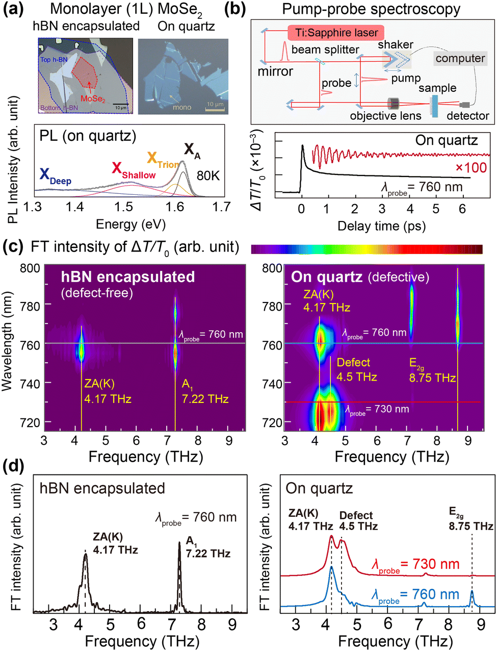 | ||
| Fig. 1 PL and CP signals of the 1L MoSe2 samples. (a) Top: Optical microscopy images of the hBN-encapsulated 1L MoSe2 (left) and bare 1L MoSe2 on a quartz substrate (right). Bottom: The PL spectra of bare 1L MoSe2 obtained at 80 K. (b) Top: The experimental pump-probe setup. Bottom: The time-resolved transmission change obtained at an excitation energy of 760 nm shown together with the magnified transmission oscillation due to CP generation (red line). (c) Fourier transformed intensity maps of the (left) hBN-encapsulated and (right) bare 1L MoSe2 samples. (d) Fourier transformed spectra of the former at the excitation energy of 760 nm and those of the latter at two excitation energies of 730 nm and 760 nm. Optical resonance and CP frequencies are denoted by dotted lines together with assigned phonon modes. | ||
Fig. 1(b) illustrates the experimental pump-probe setup (top panel) and the time-resolved transmittance signal (bottom panel) observed for the 1L MoSe2 on quartz. From the pump-probe measurements of both samples, CP signals were obtained through the Fourier transformation of time-domain oscillation of optical transmission changes (ΔT/T0) and the resulting intensity maps are shown in Fig. 1(c). Fourier transformed spectra at the probe energy of 760 nm (1.63 eV) and those of the latter at two probe energies of 730 nm (1.70 eV) and 760 nm (1.63 eV) are also shown in Fig. 1(d). As detailed in ref. 14, the 4.17 THz and 7.22 THz signals in our defect-free sample can be assigned to the ZA(K) and A’1(Γ) phonon modes, respectively. We here note that the LA(K) rather than ZA(K) mode can also be activated by using a pump laser with a broadened spectrum.13 In contrast, the defective sample exhibits two additional CP signals at 4.5 THz and 8.75 THz. Whereas the sharp 8.75 THz mode was also observed in Raman scattering measurements and can be attributed to the scattering of the E2g phonon at the Se vacancy,5 the broad 4.5 THz mode is not ascribed to the defect-induced scattering of lattice phonon modes.5,16 Accordingly, revealing the nature and atomistic origin of the defect-originated 4.5 THz CP signal will be the focus of this paper.
Before discussing the origin of the defect-related 4.5 THz mode, we first establish the correlation between the CP signals and the spatial distribution of the ZA(K) and the defect-originated modes. Fig. 2(a) displays the experimental CP spectra of the defective monolayer MoSe2 sample exhibiting signals at two CP frequencies (4.17 THz and 4.5 THz) around two excitonic absorption resonance energies (1.63 eV and 1.72 eV), which are attributed to the A exciton and defect resonance, respectively. In the experimental CP spectra, the ZA(K) mode (4.17 THz) exhibits two strong CP signals at both 1.63 eV and 1.72 eV resonance energies. On the other hand, the defect-induced CP mode (4.5 THz) exhibits a weak CP signal at the exciton resonance (1.63 eV) and the strong CP signal at the defect resonance (1.72 eV). This contrasting feature can be explained from the distinct spatial distributions of the ZA(K) and defect-originated CP modes, as illustrated in Fig. 2(c): the delocalized ZA(K) mode should displace atoms both at pristine and defect regions and thus should strongly respond to both the pristine lattice excitonic absorption (∼1.63 eV) and defect-trapped excitonic absorption (∼1.72 eV). On the other hand, the defect-localized 4.5 THz CP mode will mainly respond to the defect-centered excitonic resonance, giving a strong CP signal only at 1.72 eV.
 | ||
| Fig. 2 The experimental CP (Coherent phonon) spectra of the defective MoSe2, and its schematic interpretation of the CP signals delivered from two different coherent phonons. (a) The Fourier transformed intensity map of CP measurement obtained with the defective 1L MoSe2 on the quartz substrate. (b) Schematics of the optical spectra (absorption and transmittance spectra) of the defective MoSe2 exhibiting extrema at the excitonic resonance and the defect resonance of shallow traps (STs). (c) Schematics of atomic displacements and transmittance modulations (ΔT/T0) of the ZA(K) mode (top) and the defect-localized mode (down). | ||
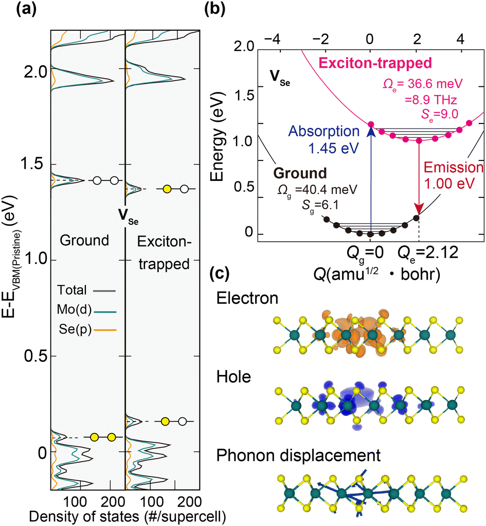
Having experimentally confirmed that the 4.5 THz CPs arise from the ultrafast carrier trappings at defects in the sub-picosecond timescale, we next clarify the atomistic origins of CP-generating and related lattice defects based on first-principles calculations. Given the huge exciton binding energy of the 1L MoSe2, the trapping of excitons at defects presumably occurs prior to the electron–hole recombination. To theoretically capture the process of the 4.5 THz CP generation after the ultrafast exciton trapping, we henceforth performed for candidate lattice defects placed in the 8 × 8 × 1 1L MoSe2 supercell (Fig. 3 insets) density functional theory (DFT) calculations. To overcome the limitations of semi-local DFT approximations in describing defect levels originating from their self-interaction error,16,17 we adopted the HSE06 hybrid functional.18 Other computational details can be found in the ESI,† Fig. S2 and Table S1. Among many candidate lattice defects, we will particularly focus on the Se vacancy (VSe) and its two defect complexes, VSe passivated by an oxygen atom (VSe + O) and an oxygen molecule (VSe + O2) for the following reasons: (1) the Se vacancy has been experimentally confirmed to be the most abundant defect type in MoSe2 owing to its low formation enthalpy (∼2 eV).19 (2) After TMDC samples are exposed to air, an oxygen molecule can be adsorbed at the Se vacancy with a large adsorption energy exceeding 2 eV.20–23 (3) The oxygen molecule adsorbed at the Se vacancy can be dissociated into oxygen atoms by overcoming a relatively small thermal energy barrier of about 1 eV.24,25
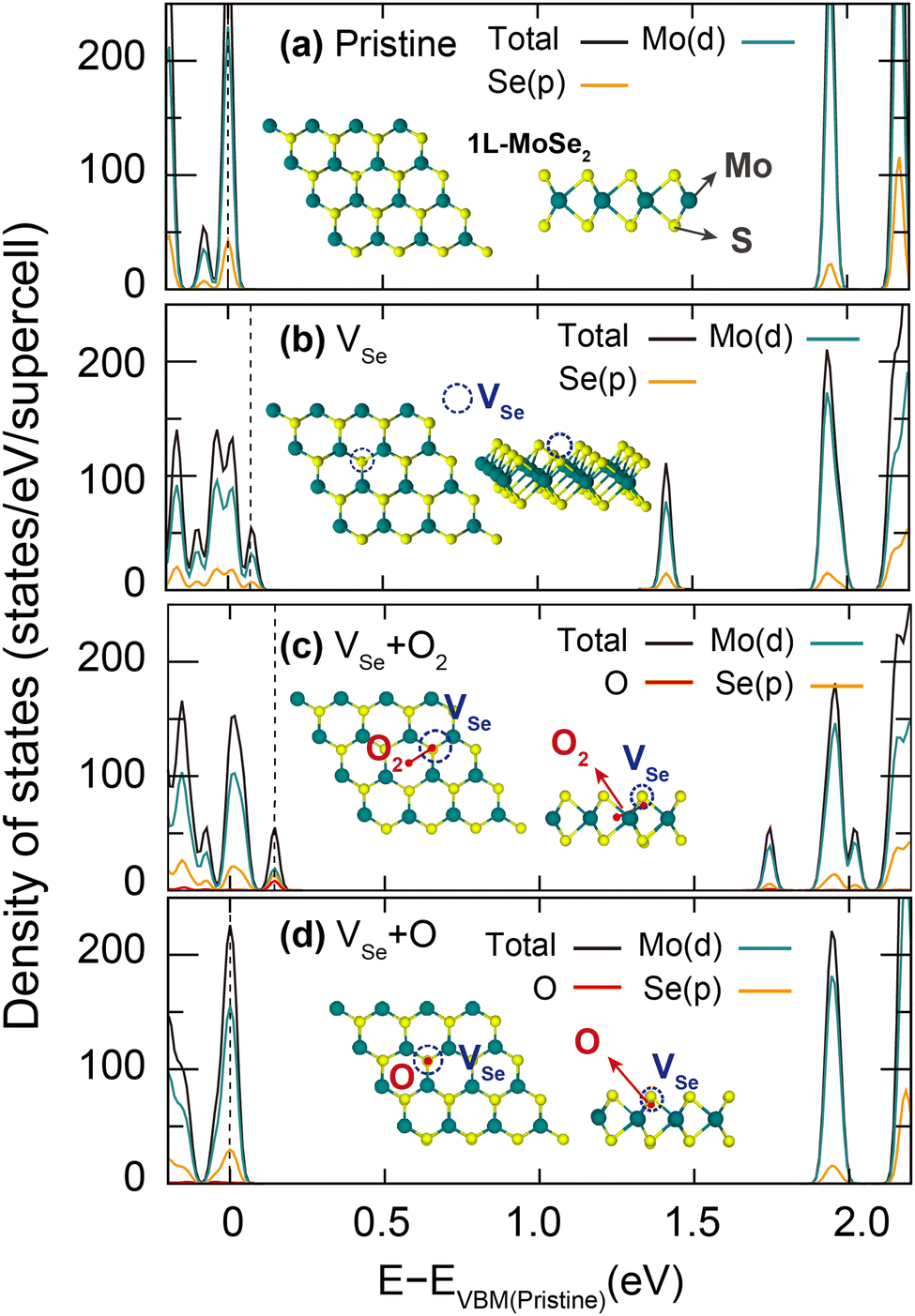 | ||
| Fig. 3 Atomic structures and ground-state DOS of pristine and defective 1L MoSe2 calculated for the 8 × 8 × 1 supercell using the HSE06 functional. DOS of (a) pristine, (b) VSe, (c) VSe + O2, and (d) VSe + O 1L MoSe2. The O atom in (d) simply passivates the Se vacancy, removing deep trap states that appeared from VSe (b). On the other hand, the O2 molecule adsorbed in (c) both passivates VSe with one O and places the other O atom at the hollow site, creating shallow trap states. | ||
Optimized atomic structures and density of states (DOS) of the pristine 1L MoSe2 and its defective counterparts (VSe, VSe + O and VSe + O2) are presented in Fig. 3. We note that, while the HSE06-calculated band gap of 1.92 eV for the pristine MoSe2 is underestimated by 0.3 eV compared to the experimental quasiparticle (QP) gap,26,27 the level of quantitative agreement is sufficient for our purpose. In the DOS shown in Fig. 3, we first find that VSe + O does not induce in-gap states owing to the substitution of a Se atom with an isovalent O atom.23,28 We can thus conclude that the VSe + O complex, which might be present in experimental conditions, is not relevant to the observed ultrafast exciton trapping at defects.28,29 On the other hand, VSe and VSe + O2 create in-gap states at the mid gap and in the vicinity of the band edges, which are presumably related to the experimentally detected deep trap and shallow trap signals, respectively.
To analyze the nature of excitons trapped at VSe and VSe + O2, we next performed occupation-constrained DFT or ΔSCF calculations.30–34 In Fig. 4(a), we present the potential energy surface diagram and spatial carrier distributions corresponding to the lattice displacements for VSe + O2 obtained from the ΔSCF occupation constraint of promoting one electron from the highest occupied level to the lowest unoccupied level. After a single exciton is formed at VSe + O2, as shown in Fig. 4(a), the defect states are shifted toward the mid-gap region, reflecting the strong coulomb attraction between holes and electrons localized around the defect.35,36 Concurrently, as shown in Fig. 4(b) and (c), the atomic structure is deformed and stabilized with a large relaxation energy of 0.168 eV. The degree of structural deformation was quantified by the generalized configuration coordinate 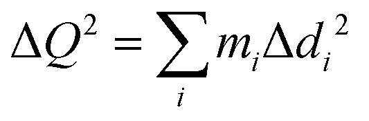 where mi and Δdi are the atomic mass and the relaxation of the i-th atom.16,35–40 As shown in Fig. 4(b) and 5(b), the potential energy surfaces of VSe + O2 and VSe are well expressed by the harmonic approximation. The phonon energy and Huang–Rhys factor were evaluated using the effective one-dimensional (1D) approximation as
 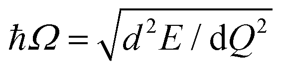 and S = ΔE/ħΩ, respectively, where ħΩ is the phonon energy and ΔE is the relaxation energy. The huge Huang–Rhys factor 9.0 of VSe + O2 indicates the strong exciton–phonon interaction in 1L MoSe2 associated with the multi-phonon emission process,37,41 which ensures the reliability of the effective 1D approximation.38,39 The calculated phonon frequency of exciton trapping at VSe + O2 is 4.5 THz (18.7 meV), which is in excellent agreement with the frequency of the experimentally confirmed defect-localized CP signal at 4.5 THz. As discussed in ESI,† Fig. S3 and the associated text, the difference between the folded oscillator strengths or absorption spectra calculated for the ground-state (Qg = 0) and relaxed excited-state atomic structures (Qe = 3.79) produces a resonance at 1.73 eV, which compares well with the experimentally observed defect resonance at 1.72 eV. We thus conclude that the shallow VSe + O2 complex defect state behaves as the ultrafast exciton trapping center in defective 1L MoSe2.
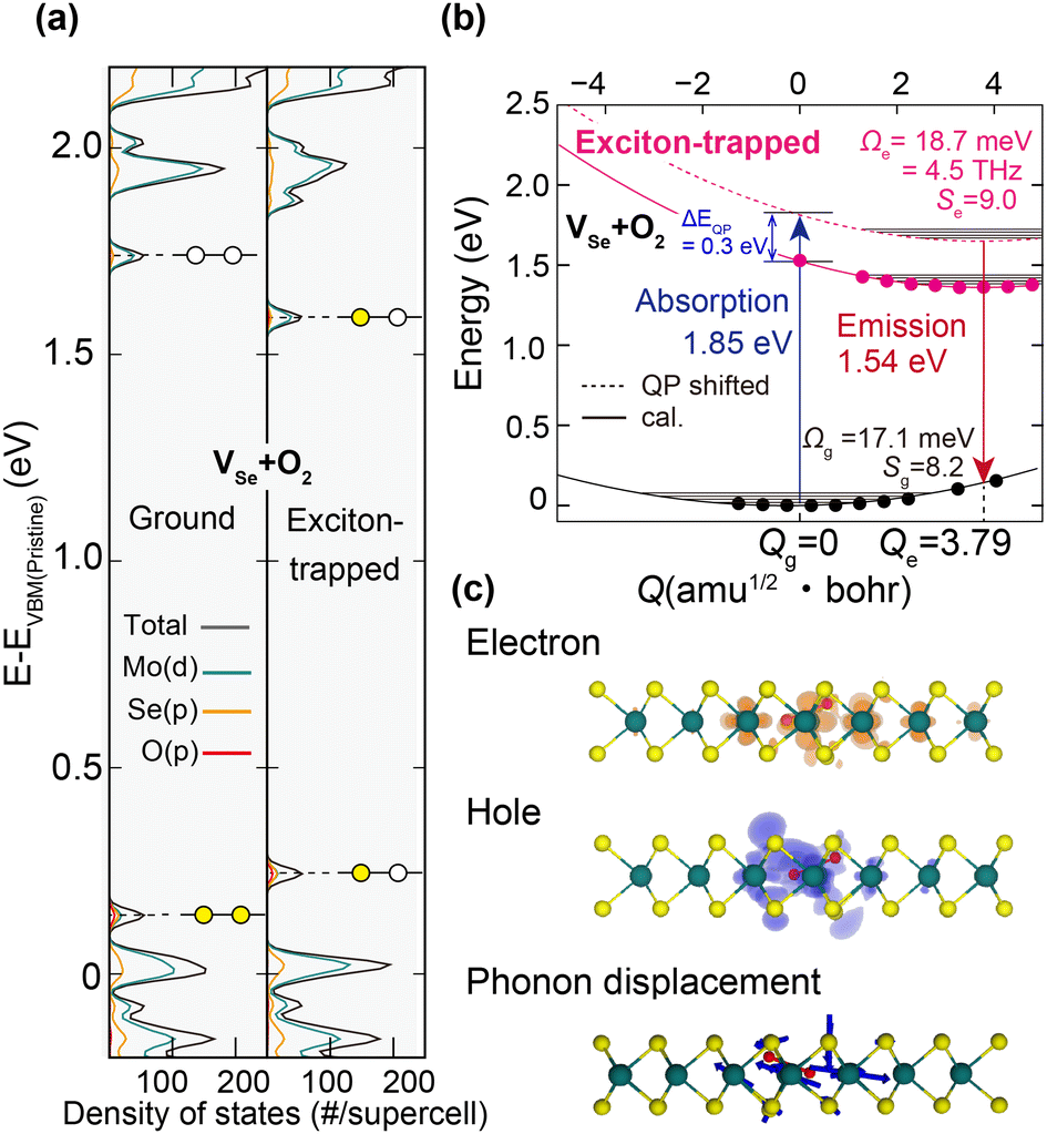 | ||
| Fig. 4 Electronic structures, potential surfaces, and atomic displacements of the exciton-trapped VSe + O2 defect complex in 1L MoSe2 calculated by ΔSCF calculations. (a) The DOS and (b) the potential energy surfaces of the ground-state and exciton-trapped-state VSe + O2. In (b), the solid line is the harmonic fitting of ΔSCF calculation results, and the dotted line is the rigid upward shift by 0.3 eV to reflect the underestimation of the QP gap of 1L MoSe2 within the HSE06 functional. (c) The charge density distribution of the VSe + O2-trapped exciton and the associated structural relaxation. Qg/e, Ωg/e and Sg/e denote the generalized configuration coordinates, effective phonon frequencies, and Huang–Rhys factors of the ground/trapped-exciton state, respectively. The iso-surface of spatial distribution plot of holes and electrons is 0.001 e Å−3. | ||
 | ||
| Fig. 5 Electronic structures, potential surfaces, and atomic displacements of the exciton-trapped VSe defect complex in 1L MoSe2 calculated by ΔSCF calculations. (a) The DOS and (b) the potential energy surfaces of the ground-state and exciton-trapped-state VSe. (c) The charge density distribution of the VSe-trapped exciton and the associated structural relaxation. Qg/e, Ωg/e and Sg/e denote the generalized configuration coordinates, effective phonon frequencies, and Huang–Rhys factors of the ground/trapped-exciton state, respectively. The iso-surface of the spatial distribution plot of holes and electrons is 0.001 e Å−3. | ||
The corresponding ΔSCF result for VSe that exhibited a deep trap (Fig. 3(b)) is also presented in Fig. 5. The calculated phonon frequency is 8.9 THz (36.6 meV) and the Huang–Rhys factor is 5.5. However, it should be reminded that such a signal was missing or the ultrafast exciton trapping at VSe was not detected in our CP measurement (Fig. 1(c), right panel). We thus conclude that, because the trapping of band edge excitons at the deep VSe defect state would be much delayed compared with the ultrafast exciton trapping at the shallow VSe + O2 defect state, VSe is incapable of producing defect-localized CP. This then establishes the condition for the trapping of excitons at defects to generate defect-localized CPs.
We finally revisit the experimental PL spectra (Fig. 1(a) bottom panel) and fit them with the above-calculated 1D parameters according to
 | (1) |
| E ZPL (eV) | ΔQ (amu1/2 Bohr) | ΔEg (eV) | ΔEe (eV) | ħΩ g (meV) | ħΩ e (meV) | S e (meV) | S g (meV) | |
|---|---|---|---|---|---|---|---|---|
| VSe + O2 | 1.68 | 3.79 | 0.140 | 0.168 | 1.71 (4.1 THz) | 18.7 (4.5 THz) | 8.2 | 9.0 |
| VSe | 1.55 | 2.12 | 0.267 | 0.204 | 40.0 (9.8 THz) | 36.7 (8.9 THz) | 6.1 | 5.5 |
3. Conclusions
In summary, performing CP spectroscopy measurements for defective monolayer MoSe2, we observed localized CPs generated from the ultrafast trapping of band edge excitons at lattice defects. Based on occupation-constrained DFT calculations, the defect-originated 4.5 THz CP signal was attributed to the VSe + O2 defect complex in 1L MoSe2 that forms the shallow trap and acts as the sub-picosecond time scale ultrafast exciton trapping center. Similar localized CPs were not observed with the VSe-originated deep trap, whereas the PL spectra indicated that excitons are annihilated also at the deep trap at longer time scales. This established that the shallow nature of a defect is a precondition for the ultrafast trapping of band edge excitons and the subsequent generation of defect-localized CPs in atomically thin 2D materials. Additional work is required for a similar observation in other 2D materials and/or the modulation of defect levels by, e.g., electrostatic gating, which will lead to the quantification of the ‘shallowness’ of defect levels. Observing the CP generation from the ultrafast trapping of band edge excitons at shallow traps in monolayer TMDCs and clarifying its atomistic origins, this work could open up novel avenues to manipulate photoexcited carriers via defect engineering.Author contributions
K.-J. Y. and Y.-H. K. conceived and supervised this project. T. Y. J. and K.-J. Y. built the optical pump–probe and photoluminescence setup and performed the experiments. S. B. performed ground- and excited-state first-principles calculations. S. B., H. R., K.-J. Y., and Y.-H. K. wrote this paper. All authors approved the final version of the manuscript.Conflicts of interest
There are no conflicts to declare.Acknowledgements
This research was funded by the National Research Foundation of Korea (2023R1A2C2003816, 2022K1A3A1A91094293, 2023R1A2C1004284, 2020R1A6A1A03047771), Korea Institute of Science and Technology (2E31801-22-027), and Samsung Research Funding & Incubation Center (SRFC-T00412003-01). S. B. was additionally supported by a Grant-in-Aid for JSPS Fellows (no. 21J15353) of JSPS and the Iwaki Scholarship Foundation. Numerical calculations were performed at the KISTI Supercomputing Center (KSC-2022-CRE-0258) and Research Center for Computational Science at ISSP and Information Technology Center, The University of Tokyo. S. B. and T.-Y. Jeong contributed equally to this work.References
- T. K. Cheng, J. Vidal, H. J. Zeiger, G. Dresselhaus, M. S. Dresselhaus and E. P. Ippen, Appl. Phys. Lett., 1991, 59, 1923 CrossRef CAS.
- G. C. Cho, W. Kutt and H. Kurz, Phys. Rev. Lett., 1990, 65, 764 CrossRef CAS PubMed.
- J. Shim, H. S. Kim, Y. S. Shim, D.-H. Kang, H.-Y. Park, J. Lee, J. Jeon, S. J. Jung, Y. J. Song, W.-S. Jung, J. Lee, S. Park, J. Kim, S. Lee, Y.-H. Kim and J.-H. Park, Adv. Mater., 2016, 28, 5293–5299 CrossRef CAS PubMed.
- V. Carozo, Y. Wang, K. Fujisawa, B. R. Carvalho, A. McCreary, S. Feng, Z. Lin, C. Zhou, N. Perea-López, A. L. Elías, B. Kabius, V. H. Crespi and M. Terrones, Sci. Adv., 2017, 3, e1602813 CrossRef PubMed.
- S. Bae, N. Sugiyama, T. Matsuo, H. Raebiger, K. I. Shudo and K. Ohno, Phys. Rev. Appl., 2017, 7, 024001 CrossRef.
- D. Edelberg, D. Rhodes, A. Kerelsky, B. Kim, J. Wang, A. Zangiabadi, C. Kim, A. Abhinandan, J. Ardelean, M. Scully, D. Scullion, L. Embon, R. Zu, E. J. G. Santos, L. Balicas, C. Marianetti, K. Barmak, X. Zhu, J. Hone and A. N. Pasupathy, Nano Lett., 2019, 19, 4371–4379 CrossRef CAS PubMed.
- H. Wang, C. Zhang and F. Rana, Nano Lett., 2015, 15, 8204–8210 CrossRef CAS PubMed.
- K. Chen, R. Ghosh, X. Meng, A. Roy, J. S. Kim, F. He, S. C. Mason, X. Xu, J. F. Lin, D. Akinwande, S. Banerjee and Y. Wang, npj 2D Mater. Appl., 2017, 1, 1–7 CrossRef.
- K. Chen, A. Roy, A. Rai, A. Valsaraj, X. Meng, F. He, X. Xu, L. F. Register, S. Banerjee and Y. Wang, ACS Appl. Mater. Interfaces, 2018, 10, 1125–1131 CrossRef CAS PubMed.
- C. He, L. Zhu, Q. Zhao, Y. Huang, Z. Yao, W. Du, Y. He, S. Zhang and X. Xu, Adv. Opt. Mater., 2018, 6, 1–8 Search PubMed.
- L. Li, M.-F. Lin, X. Zhang, A. Britz, A. Krishnamoorthy, R. Ma, R. K. Kalia, A. Nakano, P. Vashishta, P. Ajayan, M. C. Hoffmann, D. M. Fritz, U. Bergmann and O. V. Prezhdo, Nano Lett., 2019, 19, 6078 CrossRef CAS PubMed.
- Y. Wang, Z. Nie and F. Wang, Light: Sci. Appl., 2020, 9, 192 CrossRef CAS PubMed.
- S. Bae, K. Matsumoto, H. Raebiger, K.-I. Shudo, Y.-H. Kim, Ø. S. Handegård, T. Nagao, M. Kitajima, Y. Sakai, X. Zhang, R. Vajtai, P. Ajayan, J. Kono, J. Takeda and I. Katayama, Nat. Commun., 2022, 13, 4279 CrossRef CAS PubMed.
- T.-Y. Jeong, S. Bae, S.-Y. Lee, S. Jung, Y.-H. Kim and K.-J. Yee, Nanoscale, 2020, 12, 22487–22494 RSC.
- D. K. Efimkin and A. H. MacDonald, Phys. Rev. B, 2017, 95, 035417 CrossRef.
- S. Bae and H. Raebiger, Phys. Rev. B, 2016, 94, 241115(R) CrossRef.
- J. P. Perdew and A. Zunger, Phys. Rev. B: Condens. Matter Mater. Phys., 1981, 23, 5048–5079 CrossRef CAS.
- J. Heyd and G. E. Scuseria, J. Chem. Phys., 2004, 121, 1187–1192 CrossRef CAS PubMed.
- B. Huang, M. Yoon, B. G. Sumpter, S. H. Wei and F. Liu, Phys. Rev. Lett., 2015, 115, 126806 CrossRef PubMed.
- S. Tongay, J. Zhou, C. Ataca, J. Liu, J. S. Kang, T. S. Matthews, L. You, J. Li, J. C. Grossman and J. Wu, Nano Lett., 2013, 13, 2831–2836 CrossRef CAS PubMed.
- H. Nan, Z. Wang, W. Wang, Z. Liang, Y. Lu, Q. Chen, D. He, P. Tan, F. Miao, X. Wang, J. Wang and Z. Ni, ACS Nano, 2014, 8, 5738–5745 CrossRef CAS PubMed.
- H. M. Oh, G. H. Han, H. Kim, J. J. Bae, M. S. Jeong and Y. H. Lee, ACS Nano, 2016, 10, 5230–5236 CrossRef CAS PubMed.
- Y. J. Zheng, Y. Chen, Y. L. Huang, P. K. Gogoi, M. Y. Li, L. J. Li, P. E. Trevisanutto, Q. Wang, S. J. Pennycook, A. T. S. Wee and S. Y. Quek, ACS Nano, 2019, 13, 6050–6059 CrossRef CAS PubMed.
- H. Liu, N. Han and J. Zhao, RSC Adv., 2015, 5, 17572–17581 RSC.
- J. Pető, T. Ollár, P. Vancsó, Z. I. Popov, G. Z. Magda, G. Dobrik, C. Hwang, P. B. Sorokin and L. Tapasztó, Nat. Chem., 2018, 10, 1246–1251 CrossRef PubMed.
- X. Lu, X. Li and L. Yang, Phys. Rev. B, 2019, 100, 155416 CrossRef CAS.
- H.-G. Kim and H. J. Choi, Phys. Rev. B, 2021, 103, 085404 CrossRef CAS.
- S. Barja, S. Refaely-Abramson, B. Schuler, D. Y. Qiu, A. Pulkin, S. Wickenburg, H. Ryu, M. M. Ugeda, C. Kastl, C. Chen, C. Hwang, A. Schwartzberg, S. Aloni, S. K. Mo, D. F. Ogletree, M. F. Crommie, O. V. Yazyev, S. G. Louie, J. B. Neaton and A. W.-Bargioni, Nat. Commun., 2019, 10, 1–8 CrossRef CAS PubMed.
- J. Lu, A. Carvalho, X. K. Chan, H. Liu, B. Liu, E. S. Tok, K. P. Loh, A. H. Castro Neto and C. H. Sow, Nano Lett., 2015, 15, 3524–3532 CrossRef CAS PubMed.
- A. Görling, Phys. Rev. A, 1999, 59, 3359 CrossRef.
- Á. Nagy and M. Levy, Phys. Rev. A, 2001, 83, 4361 Search PubMed.
- P. W. Ayers, M. Levy and A. Nagy, J. Chem. Phys., 2015, 143, 191101 CrossRef CAS PubMed.
- J. Lee, H. S. Kim and Y.-H. Kim, Adv. Sci., 2020, 7, 2001038 CrossRef CAS PubMed.
- J. Lee, H. Yeo and Y.-H. Kim, Proc. Natl. Acad. Sci. U. S. A., 2020, 117, 10142 CrossRef CAS PubMed.
- Y. Jia, A. Miglio, M. Mikami and X. Gonze, Phys. Rev. Mater., 2018, 2, 125202 CrossRef CAS.
- S. Seo, J.-J. Lee, R.-G. Lee, T. H. Kim, S. Park, S. Jung, H.-K. Lee, M. Andreev, K.-B. Lee, K.-S. Jung, S. Oh, H.-J. Lee, K. S. Kim, G. Y. Yeom, Y.-H. Kim and J.-H. Park, Adv. Mater., 2021, 33, e2102980 CrossRef PubMed.
- A. M. Stoneham, Rep. Prog. Phys., 1981, 44, 1251 CrossRef.
- K. Huang and A. Rhys, Proc. Royal Soc., 1997, 204, 406 Search PubMed.
- A. Alkauskas, J. L. Lyons, D. Steiauf and C. G. Van de Walle, Phys. Rev. Lett., 2012, 109, 267401 CrossRef PubMed.
- A. Alkauskas, M. D. McCluskey and C. G. Van de Walle, J. Appl. Phys., 2016, 119, 181101 CrossRef.
Footnotes |
| † Electronic supplementary information (ESI) available. See DOI: https://doi.org/10.1039/d3nh00194f |
| ‡ These authors contributed equally to this work. |
| This journal is © The Royal Society of Chemistry 2023 |