
Memristor-based neural networks: a bridge from device to artificial intelligence
Zelin
Cao
ab,
Bai
Sun
 *a,
Guangdong
Zhou
c,
Shuangsuo
Mao
d,
Shouhui
Zhu
e,
Jie
Zhang
f,
Chuan
Ke
f,
Yong
Zhao
def and
Jinyou
Shao
*a
*a,
Guangdong
Zhou
c,
Shuangsuo
Mao
d,
Shouhui
Zhu
e,
Jie
Zhang
f,
Chuan
Ke
f,
Yong
Zhao
def and
Jinyou
Shao
*a
aFrontier Institute of Science and Technology (FIST), Xi’an Jiaotong University, Xi'an, Shaanxi 710049, China. E-mail: baisun@xjtu.edu.cn; jyshao@xjtu.edu.cn
bShaanxi International Joint Research Center for Applied Technology of Controllable Neutron Source, School of Science, Xijing University, Xi'an 710123, China
cCollege of Artificial Intelligence, Brain-inspired Computing & Intelligent Control of Chongqing Key Lab, Southwest University, Chongqing 400715, China
dFujian Provincial Collaborative Innovation Center for Advanced High-Field Superconducting Materials and Engineering, Fujian Normal University, Fuzhou, Fujian 350117, China
eSchool of Physical Science and Technology, Key Laboratory of Advanced Technology of Materials, Southwest Jiaotong University, Chengdu, Sichuan 610031, China
fSchool of Electrical Engineering, Southwest Jiaotong University, Chengdu, Sichuan 610031, China
First published on 8th March 2023
Abstract
Since the beginning of the 21st century, there is no doubt that the importance of artificial intelligence has been highlighted in many fields, among which the memristor-based artificial neural network technology is expected to break through the limitation of von Neumann so as to realize the replication of the human brain by enabling strong parallel computing ability and efficient data processing and become an important way towards the next generation of artificial intelligence. A new type of nanodevice, namely memristor, which is based on the variability of its resistance value, not only has very important applications in nonvolatile information storage, but also presents obsessive progressiveness in highly integrated circuits, making it one of the most promising circuit components in the post-Moore era. In particular, memristors can effectively simulate neural synapses and build neural networks; thus, they can be applied for the preparation of various artificial intelligence systems. This study reviews the research progress of memristors in artificial neural networks in detail and highlights the structural advantages and frontier applications of neural networks based on memristors. Finally, some urgent problems and challenges in current research are summarized and corresponding solutions and future development trends are put forward.
 Zelin Cao | Zelin Cao received his MS degree in Condensed Matter Physics from Southwest Jiaotong University (China) in 2020 and is working at Xijing University (China) since 2021. Currently, his main research interests are the design and manufacture of nanomaterials for memristive memory applications and understanding the microscopic mechanisms of resistance-switching using density functional theory (DFT) calculations. |
 Bai Sun | Dr Bai Sun received his PhD degree from the Faculty of Materials and Energy, Southwest University (China) in 2015 and worked at Southwest Jiaotong University since 2016. Subsequently, he conducted postdoctoral research at the University of Waterloo (Canada) from 2018 to 2021. Currently, he is a professor at Xi’an Jiaotong University. His research interests mainly focus on the development of new energy materials, preparation of memristive devices and their application in brain-like chips, neural synapses, neural networks, neuromorphic computing, quantum computing, information sensing, electronic skin, artificial intelligence, etc. |
 Guangdong Zhou | Dr Guangdong Zhou received his PhD degree from the Faculty of Materials and Energy, Southwest University (China) in 2018. He conducts his postdoctoral research at Southwest University. His research focus is on the physical mechanisms of memristors and memristor-based functions, including memory logics, displays and synapses. His memristor-related research is supported by the Postdoctoral Program for Innovative Talent Support of Chongqing. In the past 10 years, he has published more than 80 peer-reviewed papers. |
 Shuangsuo Mao | Shuangsuo Mao is pursuing his PhD Degree at the College of Physics and Energy, Fujian Normal University (China). He received an M.S. degree in Condensed Matter Physics from Southwest Jiaotong University in 2020. His research focus is on the design of memristive devices and the fabrication of nanomaterials for memory applications. |
 Jinyou Shao | Dr Jinyou Shao received his PhD degree from Xi’an Jiaotong University, Xi’an, China, in 2009. He is currently a professor at the State Key Laboratory for Manufacturing Systems Engineering, Xi’an Jiaotong University. His research interests include micro/nanomanufacturing techniques, flexible electronics and systems, nanosensors and devices. Prof. Shao received the First Prize Technology Invention Award from the Ministry of Education of China in 2015. He has been awarded Changjiang Scholars –Young Category, NSFC Fund for Excellent Young Scholars, New Century Excellent Talents by MoE of China, Shaanxi Young Talents in Science and Technology, ACS Membership Award, etc. |
1. Introduction
1.1 Memristor
In 1971, Chua believed that there should be a circuit component that can reveal the relationship between the magnetic flux and the charge,1 which was defined as a memristor. Thus, the memristor, also known as a memory resistor, is considered the fourth fundamental passive circuit component other than the resistor, capacitor, and inductor. The resistance values of the memristor can be continuously adjusted under an applied voltage, and its resistance states are determined by the flowing current or applied voltage. According to the relationship between the four basic variables: voltage (v), current (i), charge (q) and flux (φ) (Fig. 1a), the functional relationship between charge and flux is derived as M = dφ/dq. Here, the charge is the integral of current over time, which can be expressed as dq = idt. The flux is the integral of electromotive force or voltage over time, and it can be expressed as dφ = vdt. Hence, memristance can be deduced as M = vdt/idt = v/i. According to Ohm's law, the memristance (M) at time t0 is determined by the accumulation of electric charge in the time period from the initial time to t0. Therefore, a memristor is a kind of resistive device with nonlinear resistance values in theory. However, for a long time after the memristive theory was proposed, the existence of memristor was not experimentally proven. In 2008, Strukov et al. linked the memristive theory with an experimental phenomenon in a double-layer TiO2 thin-film-based device,2 in which a hysteresis loop appeared under an applied bias voltage, which is the first proof of the existence of the memristor (Fig. 1b). Since then, memristive technologies have flourished, ranging from material systems and physical mechanisms to advanced algorithms.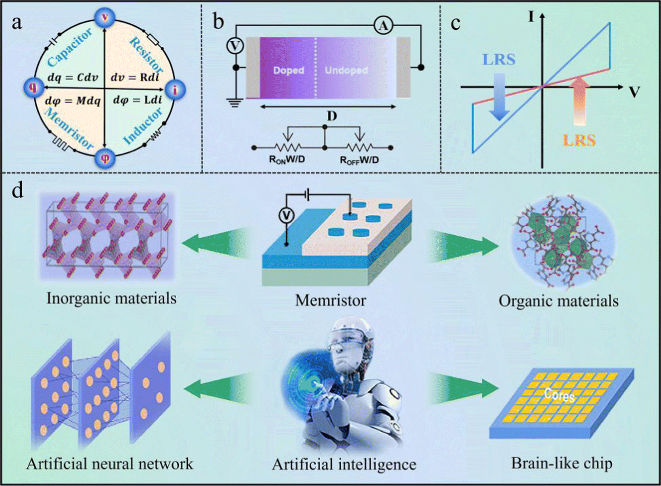 | ||
| Fig. 1 (a) Schematic of the relationship between the four basic circuit components. (b) The coupled variable-resistor effect of a memristive device based on the TiO2 film. Panel b is reproduced with permission.2 Copyright 2008, Nature Publishing Group. (c) The hysteretic I–V characteristic curve corresponding to the resistive switching effect. (d) Schematic of the memristor, in which the functional layer is made of inorganic and organic materials, used to build neural networks for artificial intelligence and brain-like chips. | ||
The resistance values of a memristor can be changed under an applied voltage or current, that is, it can memorize the flowing current in the device by changing its resistance states. The most common structure of a memristor is a sandwich composed of metal/insulator/metal layers. The top and bottom metal layers are used as the top electrode and the bottom electrode, respectively, and the middle layer is used as the functional layer of the memristive device. The memristor usually exhibits a zero-crossing current–voltage (I–V) hysteresis loop arising from the resistive switching characteristics. Under the action of an external electric field (direct current or pulse signal), the memristor can undergo a reversible transition between the high-resistance state (HRS) and the low-resistance state (LRS), as shown in Fig. 1c. The conductance of the memristor increases under the action of the applied voltage, which is known as the SET process, while it is called the RESET process when the conductance decreases under the action of reversed voltage.3–5 Depending on the polarity of the switching voltage, memristors can be divided into bipolar and unipolar resistive switching devices.6 The direction of bipolar resistive switching relies on the polarity of the applied voltage, while the direction of unipolar resistive switching is only determined by the applied voltage.
The resistance-switching characteristics of memristive devices are closely related to the electrode and functional layer materials, that is, the same electrode when combined with different functional layer materials can present different resistance-switching behaviors and mechanisms. In other words, the same functional layer materials yield different resistance-switching behaviors with different electrodes. At present, researchers have realized the preparation of memristors based on a variety of materials, such as TiOx,7 ZnO,8,9 VO2,10 TaOx,11 HfOx,12 and AlOx.13 The composition of metal oxides is simple, easy to prepare, and compatible with complementary metal oxide semiconductor (CMOS) devices.14 In addition, there are solid electrolyte materials with lattice defects and rapid ion migration, such as Ag2S,15 SiO2,16–18 and Cu2S.19 Besides, organic materials with good flexibility and low cost, such as PVP,20 PMMA,21 and PFO,22 have also been used to prepare memristive devices. Nowadays, the preparation of memristive devices can be achieved using many physical and chemical methods, such as atomic layer deposition, spin-coating method, magnetron sputtering, sol-gel method, pulsed laser deposition, and so on.23–26
In recent years, with the gradual improvement in the preparation and performance of memristors, the research focus has shifted from the preparation of devices to the development of artificial intelligence systems, neuromorphic devices and brain-like chips (Fig. 1d). Owing to the various excellent electrical properties of memristors, researchers have realized different applications, including memory circuits, logic operations, neural networks, nonlinear systems, and so on.27–31 Pi et al. reported a 3 × 3 memristor array with the Pt/TaOx/HfO2/Pt structure and feature size of 2 nm,32 demonstrating extremely high scalability, which facilitates the implementation of storage and computing systems with low power consumption and high density. Besides, a diffusion dynamics-based memristor has been developed,33 in which the dynamic process of Ag nanoparticles doped into the oxide dielectric layer is similar to the biodynamics of Ca+ ions in chemical synapses, suggesting that this memristor is capable of naturally simulating bio-synaptic behaviors, such as short-time plasticity (STP), paired-pulse facilitation (PPF), long-term plasticity (LTP), and spike-timing-dependent plasticity (STDP). Based on the above synaptic properties, artificial nociceptors and artificial sensory alarm systems can be also constructed and designed using diffusion-type memristors, thus indicating the possibility of its application in bionic robots. Further, Wong's group constructed a neuromorphic vision system with low power consumption and high fault tolerance based on a stacked oxide synaptic device,34 simulating the orientation detection function of the visual cortex of the human brain. Miao et al. researched the application of memristor-based logic operations35 and have successfully designed the memristor arithmetic logic unit, logical operations, n-bit full adders, and various operation functions. Using this logic unit, a high-performance processor with reconfigurability, low power consumption, and small size was constructed. Besides, this device exhibited near-zero static power consumption due to its integrated memory-computing feature.
Therefore, memristor devices have great potential for application in neuromorphic systems, among which memristor-based neural network is one of the focus areas in current research.36–38 The advantages of memristors in the simulation of synapses and neural networks make them one of the most ideal devices used in neuromorphic computing for artificial intelligence applications. In this paper, memristors fabricated from different materials are reviewed for basic performance characteristics, the connection with neural networks, and their application in artificial intelligence. Furthermore, the current challenges are summarized and some strategies are proposed. The schematic in Fig. 2 presents an overview of this review.
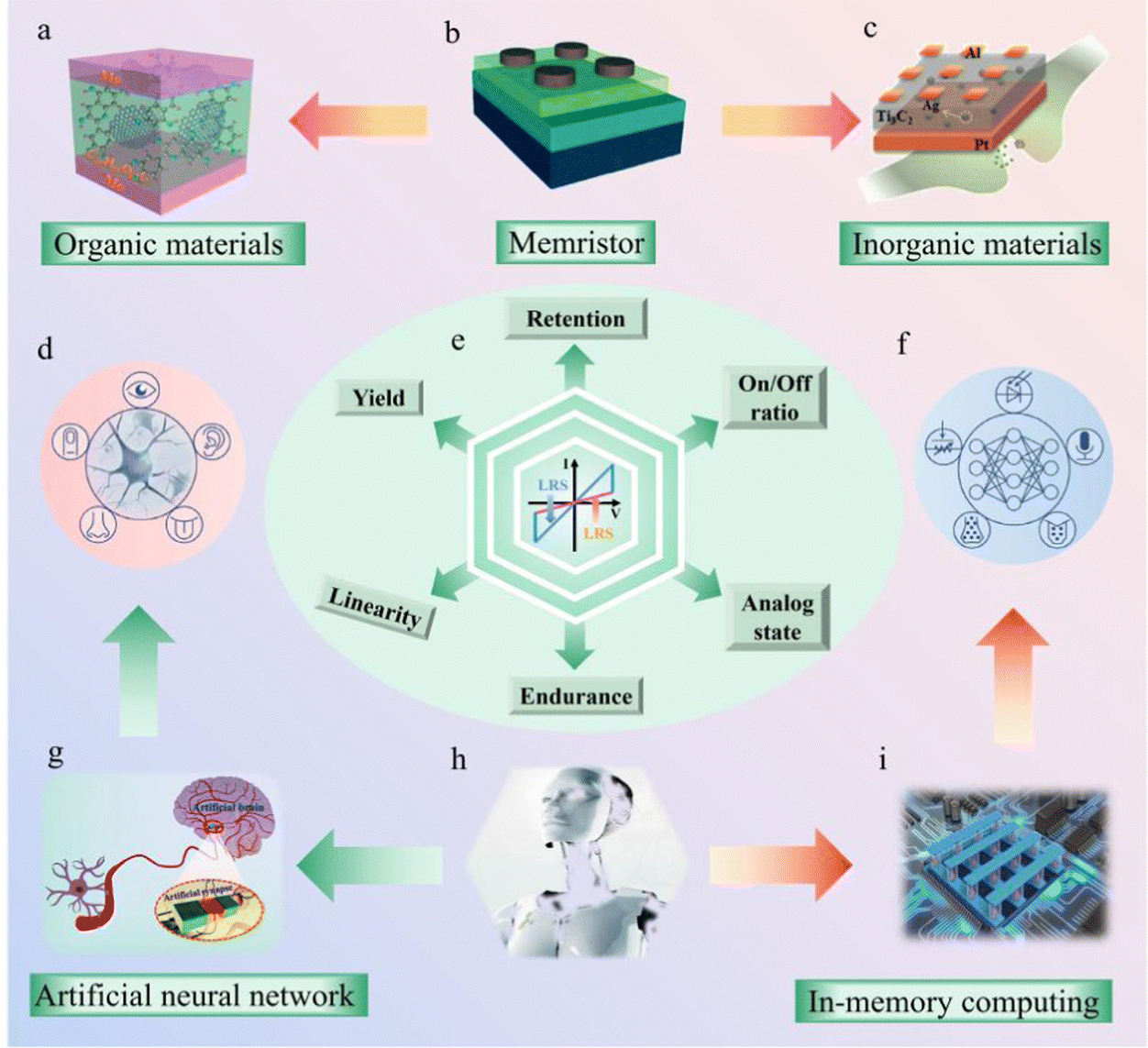 | ||
| Fig. 2 Material classification and applications of memristors. (a) The schematic of organic materials. Panel a is reproduced with permission.39 Copyright 2021, American Chemical Society. (b) The memristor structure. (c) The schematic of the inorganic material. Panel c is reproduced with permission.37 Copyright 2021, Elsevier. (d) Brain neural networks and perception. Panel d is reproduced with permission.24 Copyright 2022, Elsevier. (e) The metric parameters of a memristor. (f) An artificial multisensory neural network. Panel f is reproduced with permission.24 Copyright 2022, Elsevier. (g) Artificial neural network and artificial synapses. Panel g is reproduced with permission.39 Copyright 2021, American Chemical Society. (h) An artificial intelligence robot. (i) Schematic diagram of In-memory computing. | ||
1.2 Memristor-based neural networks
The successful preparation of artificial brain-like chips has always been considered the basis for the development of supercomputers because the human brain is the best-known computing system with superb parallel computing capability. It is generally believed that the main computational unit of the human brain is the neuron, which receives external input signals through dendrites and transmits signals to other neurons via connections called synapses. A key feature of the bio-synapse is that it can scale the signals that pass through, and the scale factor is called weight. The learning behavior of the human brain is considered to be based on the process of changing the relevant synapse weight.36,40 At present, the artificial neural network is considered the core algorithm of artificial intelligence represented by deep learning. Neural networks can perform a weighted summation of all input signals in the process of calculation. The deep hierarchical nonlinear processing of neural networks enables automatic and efficient learning of senior abstract representations in higher dimensional data, which has revolutionized the multimedia fields, such as images and videos,41 speech and language.42 It also plays an increasingly important role in the emerging fields of medical health and robotics.43–45 With continuous performance improvement, neural networks are increasingly deployed in some practical industrial applications, including manufacturing, asset management, mobile phone voice assistance, autonomous driving, and so on. Therefore, using memristors to simulate synapses is considered one of the key steps to building artificial neural networks.Nowadays, although artificial neural networks have been proposed to solve the von Neumann bottleneck,46,47 the algorithm of artificial neural networks is still based on traditional computers, which leads to a series of problems, such as limited computing power and low energy efficiency. With the advent of artificial intelligence, the internet of things and machine learning, the demand for computing power has increased exponentially. For example, for the AlphaGo implemented using 1200 central processing units (CPUs) and 180 image processors (GPUs), the power consumption is as high as hundreds of thousands of Watts.48 During the learning phase, most of the energy consumption is dedicated to the programming operations of the memory and the reading operations of the synaptic devices. Therefore, energy per operation is a key factor for estimating the energy efficiency of neuron-inspired computing chips. A neural network system composed of ∼1011 neurons and 1015 synapses can process a large amount of information with very low power consumption (20 W), and the operation consumption per stimulus is only 1–100 fJ.47,49 Nowadays, most resistive random access memory (RRAM) devices show programming energy of around 100 fJ–10 pJ, while most phase change memory (PCM) devices have higher programming energy of 10–100 pJ. On the other hand, because the memristive device has a very high stack density (<2 nm), and the switching speed can be very fast (<0.1 ns),32,50 it only needs a small amount of energy and can be manufactured in a smaller size. However, the complex manufacturing process and high energy consumption bring huge difficulties to large-scale integrated circuits. The schematic of a memristor in which the functional layer can be made of inorganic and organic materials is shown in Fig. 1d, and the memristor can serve as the core hardware for both brain-like chips and artificial intelligence algorithms. In order to effectively implement neural network algorithms, more promising hardware needs to be developed, and memristors are expected to be a central component of the new hardware. The memristor has great advantages compared with traditional devices used in the construction of neural networks. The resistive switching behavior of memristors can be divided into two types according to the resistive changes: analog type and digital type. Among them, the resistive state of the analog-type memristor is continuous, and its conductance can be gradually changed via electrical pulses, which can be used to simulate the continuous change in bio-synaptic weights and bio-neuronal membrane potential under external stimulation.51 However, the resistance states of the digital type memristor are discrete during the scanning of the voltage and can be converted between the HRS and LRS, thus achieving sudden binary conductance states for simulating all or no characteristics of the neuron network. Different memristors can also exhibit abhorrent retention characteristics, that is, the slow change in electrical conductivity in the device is similar to the process of enhancing and inhibiting the connection strength of bio-synapses. In addition, being a type of two-terminal device, the memristor has a similar structure to the neural synapse. The size of the memristor can be reduced to the nanometer level, and the integrated array density can even reach the density of the bio-synapses in the brain, which gives the memristor a distinct advantage in neural network construction. In terms of transmission mechanisms, the synapse is typically composed of a presynaptic neuron, a postsynaptic neuron, and a synaptic gap. The synapse enables signaling and behavioral changes through the transmission of Ca2+ ions and K+ ions. The top electrode, bottom electrode and functional layer of the memristive device correspond to the bio-synaptic structure.52 Interestingly, the memristor can also regulate conductance by varying the migration of ions in the functional layer. At present, in most memristors, the change in electrical conductivity is the result of ion movements, such as the migration of metal ions, oxygen vacancies and carriers captured at the interface. Therefore, the memristor is capable of acting as an electronic synapse and can be further applied in the construction of artificial neural networks.53 With the development in recent years, it has been found that memristors can achieve a variety of synaptic functions, especially in learning and memory. Nevertheless, memristors still have some challenges in realizing the perfect bio-synaptic simulation. The fundamental challenge is that it is much more difficult (thus paying more energy) to move the ions/defects in solid-state devices than the movement of Ca+ ions in a liquid environment as in bio-synapses. Fig. 3 shows the principle of a memristor used to simulate a bio-synapse and its analogy with the bio-synapse.
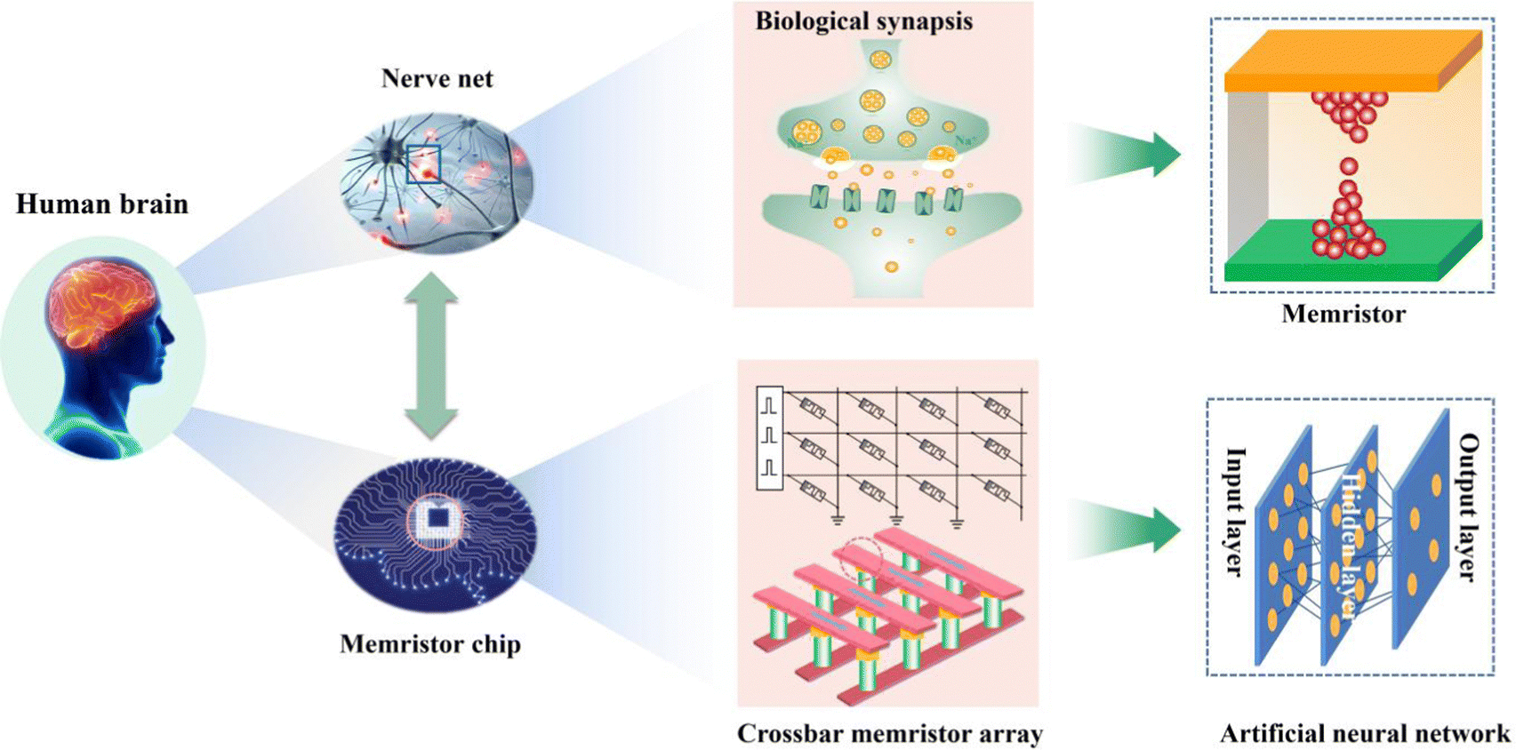 | ||
| Fig. 3 Analogy between memristor-based artificial neural networks and the synapse-based nerve net. | ||
In the neuromorphic hardware system, neural networks are divided into artificial neural networks (ANN) and spike neural networks (SNN). ANN can be extended to deep neural networks (DNN) and convolutional neural networks (CNN). In SNNs, artificial synapses are used to simulate STDP for unsupervised learning.54 To apply DNNs to achieve high recognition accuracy, it is necessary to develop artificial synapses with ideal synaptic characteristics. The synaptic characteristics of artificial synapses, such as dynamic range, multi-level states, nonlinearity, cycle-to-cycle variation, and device-to-device variation in weight update, will affect DNN accuracy.47 In general, brain-inspired neural network synapses require memristors with a wide dynamic range to accommodate a large number of resistive states. Low fluctuation, low drift and high absolute resistance value are required for precision computing while high endurance is needed during training/programming.53 In SNNs, artificial synapses are used to simulate STDP for unsupervised learning, which cannot guarantee high performance in general learning tasks.54,55 Therefore, SNNs are more suitable for low-precision computing applications. SNNs are mostly bio-plausible, real-time, less power-consuming, and suitable for brain-inspired computing systems. Hence, the synaptic plasticity of memristors is required in SNNs. ANNs have fast computing speed and high computing intensity, so they are suitable for the von Neumann computing system. For ANNs with a few layers (one or two layers), analog conductance with a wide dynamic range and high retention is an indispensable factor. Furthermore, effective neural network training also requires lower device variation and symmetrical weight update. For DNNs and CNNs, the synaptic weight is adjusted during training. In this process, increasing the number of data states can improve the learning ability and accuracy of the neural network. The weight update feature will be linear and symmetrical in order to change the synaptic weight to the desired value during training. Therefore, long retention, low power, good scalability and large dynamic range are also required characteristics of the device in addition to analog conductance.56
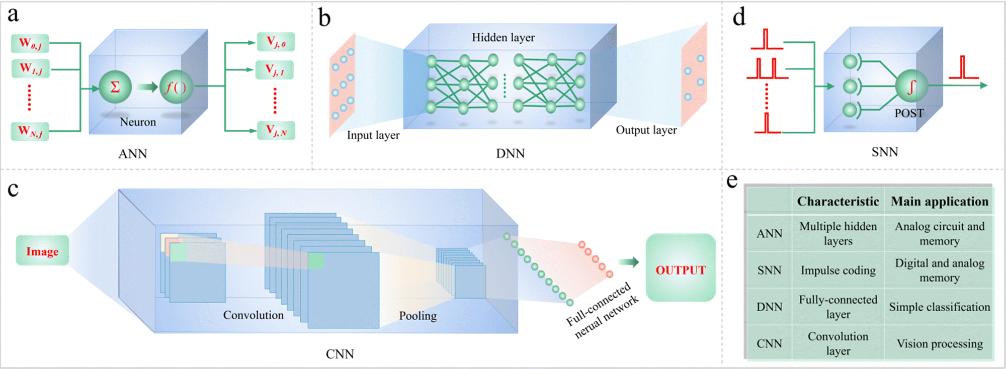 | ||
| Fig. 4 The backbone architectures of various neural networks. (a) ANN; (b) DNN; (c) CNN; (d) SNN. (e) The comparison of characteristics and main applications between ANN, DNN, CNN and SNN. | ||
The neural network has two working mechanisms: one is the inference process, and the other is the learning process, which is also known as the training process. A loss function is generally constructed to characterize the convergence degree of the model during the training process. In each hidden layer, the error derivative of each output unit is first calculated, which is the weighted sum of the error derivatives of the total input for the unit in the previous layer. Then, the output error derivative is multiplied by the gradient of the activation function f(z), thereby converting the output error derivative into the input error derivative.68–70 In the output layer, the derivative of the unit output error is calculated by a differential loss function. During the training process, the training algorithm is generally combined with some optimization algorithms to make the network weights converge to an optimal solution. In the inference process, the total input z of each neuron is calculated in each layer, and this total input is the weighted sum of all the outputs from every neuron in the front layer. Then, the total input z is used as the output of the neurons in this layer after being acted upon via the nonlinear function f. The output of each neuron layer is used as the input of the neurons in the next layer, and the final output is transmitted to the output layer. In the training process, the model first performs the forward inference process to output the decision, and then back-propagates the error and updates the weights of the model accordingly.71,72 The weights of the model are invariant during this process. Therefore, the neural network must perform a large number of matrix-vector product operations during inference and training, placing huge computational power demands on the hardware.
1.3 The development of memristor-based neural networks
The memristor-based neural networks under different information coding mainly include ANNs and SNNs. Among them, the ANN pursues higher computational efficiency in data-intensive tasks, while SNN provides excellent power efficiency by simulating biological neural networks with peak-time encoded neuron values. In the aspect of algorithm training, ex situ and in situ training are the two main training methods used in the neuromorphic simulation. In the ex situ method, the data are trained in the software system, and then, the calculated weights are loaded into the analog memristor array, demanding higher requirements of retention, bit yield, and uniformity. In contrast, a neuromorphic computing system with in situ training can update the weights on the chip, and thus, it has better immunity to retention degradation, state-stuck issues, and variations than ex situ training. On the hardware side, the basic operations of the classical ANN hardware are limited to multiplication, addition, and activation, which can be performed even by CMOS circuits (such as GPU). However, for neural networks with a large number of computational parameters, although the CMOS circuit is scalable, it still cannot match the neuromorphic simulation of the ANN. At present, many topology-learning algorithms have been developed based on ANN software and hardware. In 2018, high-precision analog tuning and control of a memristor with 128 × 64 1M-1T Ta/HfO2 array were demonstrated.83 The memristor-based system exhibited an image recognition accuracy of 89.9% for the MNIST digit set. In 2019, a WO3−x-based memristor with coexisting analog and digital resistance switches was realized, and a new analog-digital hybrid ANN memristor was further developed.84 This device demonstrated adjustable learning accuracy and speed in pattern recognition and simulates STDP learning. In 2020, a memristor crossbar was used for full hardware implementation.85 A five-layer CNN was constructed by integrating 2048 memristor array units to realize MNIST10 image recognition, and a high precision of more than 96% was achieved. In addition, this memristor array demonstrated the replication and parallel processing of multiple identical kernels, which was more than two orders of magnitude more efficient than the most advanced graphics processing units of the time, and could be scaled up to larger networks. In 2021, Wang et al. integrated photosensing, storage, and in situ computing into the memristor array, greatly improving the integration of hardware and the efficiency of the chip.86 The accuracy of the photoelectric memristor in neuromorphic computing was up to 86.7% via recognizing the facial images of different people. In addition, the integrated memristor demonstrated the attractive biomimetic sensor-in-sensor computing behavior of the photoelectric memristor, providing a possibility for the application of the photoelectric memristor in the next generation of reconfigurable sensor-memory-computing integrated paradigm. Recently, a new system inspired by neural modulation in the brain has been proposed, in which the trained synapses are temporarily hidden during the training of the spiking neural networks and then merged for inferencing.87 The self-recirculating and non-electrostatic memristor unit was integrated onto 32 × 32 medium-density polyethylene for hardware demonstration. The energy consumption of the memristor array was reduced by 37% for unsupervised learning of the MNIST dataset, which can be used in spiking neural networks for efficient learning.The third-generation SNN, which is inspired by the animal brain, enables the simulation of the desirable properties of compact biological neurons and presents significantly improved cognitive and computational performance. The most striking feature of the SNN is that it incorporates the concept of time into operations with discrete values. Many attempts have been made to implement STDP in artificial synaptic chips because the temporal and spatial variables are crucial for computing information in SNNs. Li et al. simulated 128 × 64 vector matrix multiplication using a reconfigurable HfO-based memristor crossbar switching, whose array size was up to 128 × 64 units.88 This 1T-1R memristor demonstrated high-precision image compression and convolutional filtering. In 2021, a novel CuS/GeSe memristor was proposed to realize electron-randomized neurons according to the randomness in biological ion channels.89 Compared with the SNN based on deterministic neurons, this SNN system could estimate the uncertainty in prediction and the fidelity of judgment greatly improved by 81.2%. Recently, a HfO2-based OxRAM memristor was stacked on a Ge–Se–Sb–N-based ovonic threshold switch (OTS) back-end selector for the implementation of high-density binarized SNN synaptic weight hardware.90 This memristor-based system was optimized for 1S1R low-reading bit error rate in high-frequency reasoning. For the MNIST handwritten digit recognition task, a general guide was given to reduce the system footprint and power consumption for maximizing the inference frequency and accuracy.
2. Research progress
2.1 Inorganic memristor-based neural networks
MXene is a novel 2D transition metal carbonitride belonging to the carbide and nitride family, and has become a promising 2D material in the fields of energy conversion and storage due to its interesting physical and chemical properties.98 As an emerging member of the 2D material family, the MXene Ti3C2 has received extensive attention due to its excellent memristive properties and miniature size. Wang et al. improved the electronic properties of 2D-MXene Ti3C2-based memristors via doping Ag nanoparticles into the functional layer,37 and the structure of the as-prepared memristor is shown in Fig. 5a. Compared with pure Ti3C2-based memristive devices, the Ag-nanoparticle-doped device exhibited bidirectional continuous current-transition behavior. Fig. 5b shows that the peak energy consumption of the Al/Ti3C2:Ag/Pt device was as low as 0.35 pJ, which enables the unique simulation of synaptic behaviours, including short-term memory (STM) and long-term memory (LTM) characteristics, as shown in Fig. 5c. In addition, several decimal arithmetic operations were demonstrated in the Al/Ti3C2:Ag/Pt memristor (Fig. 5d). Further, Zhang et al. demonstrated a hybrid ferroelectric Cu/MXene/PZT memristor, in which the 2D MXene material Ti3C2 intercalated into conventional PZT to improve the performance of the ferroelectric memristor.99 In contrast, the Cu/Ti3C2/PZT/Pt-based ferroelectric memristor exhibited superior characteristics, such as lower switching voltage, reproducible RS behavior, lower power dissipation and a higher on/off ratio of up to 106,99 as shown in Fig. 5e. In addition to simulating bio-synapses, the device also demonstrated the PPF and STDP functions, as illustrated in Fig. 5f. In particular, the learning and recognition accuracy for images was as high as 95.13% (Fig. 5g). Sokolov et al. applied MXene (Ti3C2Tx) sheets to electronic synapses based on their unique insulating properties,100 which led to the threshold-shift switching properties because of Ag+ ions migration kinetics. Using Ag+ ions migration, the kinetic behaviour of Ca2+ ions in the bio-synapses can be simulated. The bio-synaptic functions, including PPF, strong electric post-enhancement (PTP), STP and LTP, were further realized, as shown in Fig. 5h.
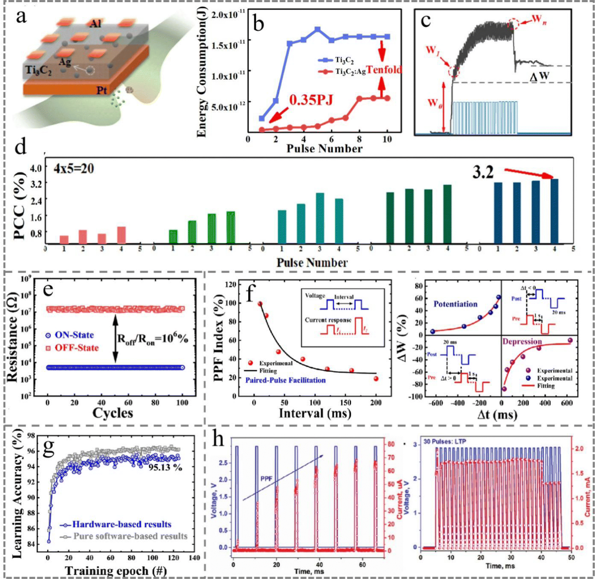 | ||
| Fig. 5 (a) The structure of the Al/Ti3C2:Ag/Pt memristor. (b) The energy consumption variation in Ti3C2- and Ti3C2:Ag-based memristive devices. (c) The implementation of memory properties and the modification of wn/wl with various pulse durations for STM and LTM. (d) The demonstration of commutative multiplication arithmetic on the Al/Ti3C2:Ag/Pt memristive device. Panels (a–d) are reproduced with permission.37 Copyright 2020, Elsevier. (e) The endurance test of the Cu/Ti3C2/PZT/Pt memristor shows the on/off ratio for 100 cycles. (f) The simulation of the typical PPF (left) and STDP (right) behaviors of the bio-synapse; the insets display the pulse protocols. (g) The neural network learning accuracy of the MXene-PZT-based memristor. Panels (e–g) are reproduced with permission.99 Copyright 2022, Elsevier. (h) Experimentally emulated PPF phenomenon (left) and artificial synaptic memory properties during the STP-to-LTP transition of the MXene-based memristive device (right). Panel h is reproduced with permission.100 Copyright 2021, Elsevier. | ||
In addition to Ti3C2, other MXenes have also been used in the construction of memristor-based artificial neural networks. In 2021, Wang et al. designed and constructed a multimodal MXene-ZnO memristive device that combined visual sensing, relative humidity sensing and preprocessing to simulate the unique visual behavior of the human eyes,101 as shown in Fig. 6a. The resistive switching behavior of the multi-field-controlled MXene-ZnO-based memristor depended on the formation of oxygen vacancy filaments via photon or proton tuning. The data collected from a single device over 100 scanning cycles and the predicted statistical distribution of the resistance ratio are shown in Fig. 6b. The time variability of the on/off ratio in the positive scan and the negative scan was 0.396 and 0.452, respectively. Fig. 6c provides the corresponding current values of the memristive device at different bending angles. The reading currents in the two conductance states were stable in the cycle of four different curvatures, proving the feasibility of its application as a flexible sensing memristor. The MXene-ZnO-based memristor with an in-sensor computational function can be used both as a sensor for information preprocessing and a synapse for the weight-updating process under environments with different humidity. To exploit the high-efficiency neuromorphic hardware networks, a multifunctional neuromorphic device based on 2D-MXenes has recently been proposed.102 This device can be programmed to achieve synaptic or neuronal functions, thus breaking the boundaries between neurons and synaptic modules and enabling efficient neuromorphic networks. The structure of the memristive device with the Ag/2D-MXene (Ti3C2Tx)-doped polyvinyl alcohol (PVA)/indium tin oxide (ITO) structure is shown in Fig. 6d. A neural network composed of multiple neuron-synaptic transistors was designed for authenticity data recognition. The hardware sources of the neuromorphic device could be uniformly redistributed, and the topology structure of the memristor array could be adjusted. This design increased the computing speed and reduced the number of devices. Fig. 6e depicts the implementation of the artificial synaptic simulation based on the as-prepared memristor. Based on this design, a hardware system was developed with a recognition accuracy of about 80%, which can be applied for face recognition (Fig. 6f).
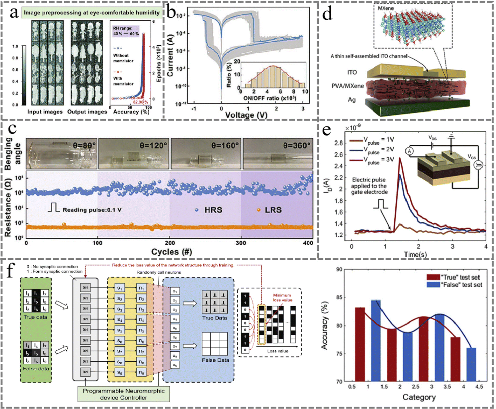 | ||
| Fig. 6 (a) The output image of the simulated artificial retinal sensing system and its image recognition rate after preprocessing (right). (b) The resistive-switching characteristics of the memristive device with the statistical switching ratio distribution. (c) The on/off current in the LRS and HRS at a read voltage of +0.1 V. The upper panel exhibits the optical images of the memristors at different bending angles. Panels (a–c) are reproduced with permission.101 Copyright 2021, Wiley-VCH. (d) Schematic of the switchable neuronal-synaptic transistor and the molecular structure of MXene. (e) The excitatory post-synaptic current triggered by the pre-synaptic pulse as a function of time. (f) The structure of the hardware networks with the neuromorphic (left) and image-recognition accuracy of the switchable neuronal-synaptic transistor system (right). Panels (d–f) are reproduced with permission.102 Copyright 2022, Elsevier. | ||
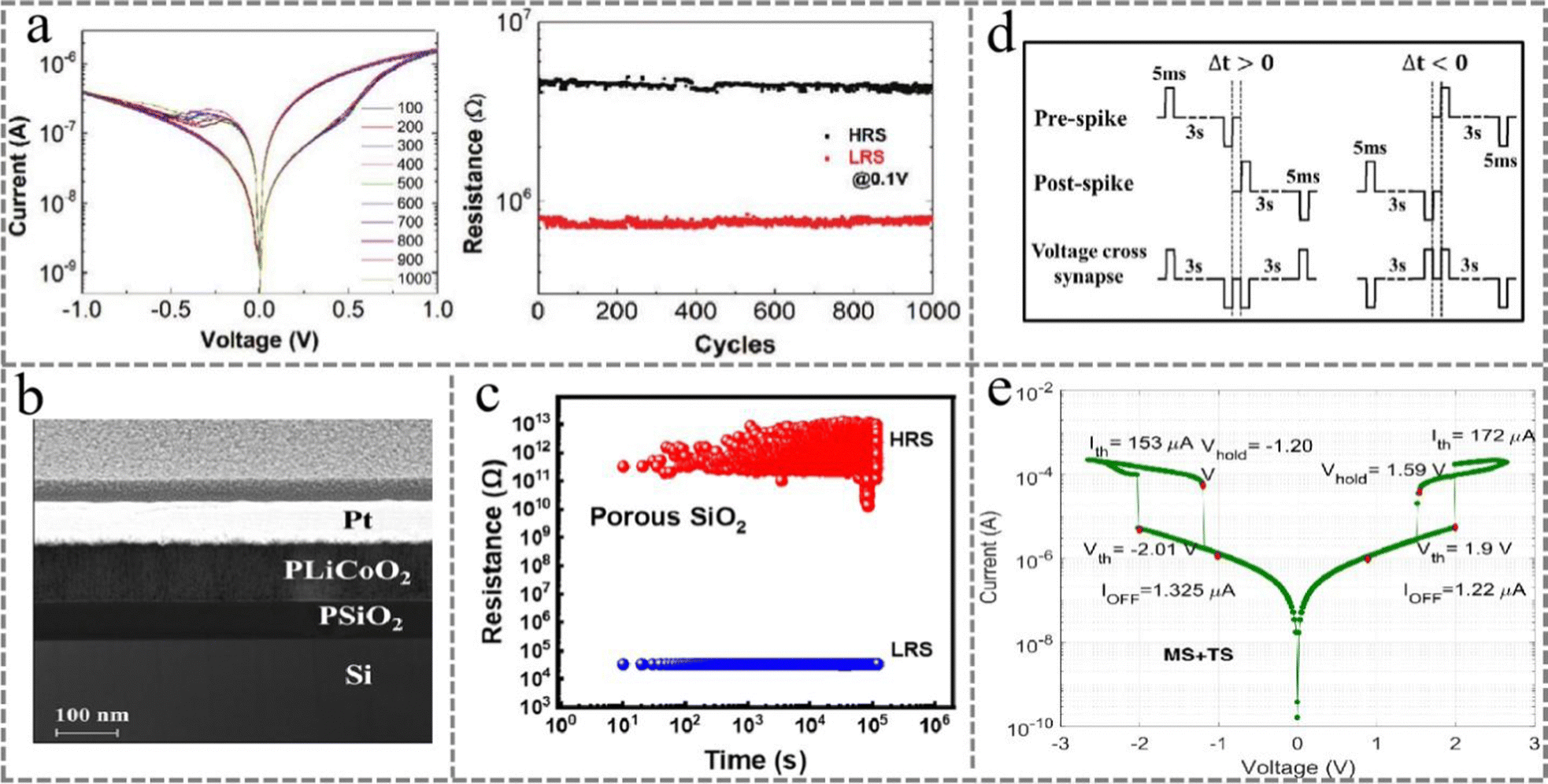 | ||
| Fig. 7 (a) The I–V curves and resistance test of HRS and LRS per 100 cycles over 1000 switching cycles. Panel a is reproduced with permission.103 Copyright 2020, Wiley-VCH. (b) A memristor with the Pt/LiCoO2/SiO2/Si structure. (c) The stability of the memristive device with the Pt/LiCoO2/SiO2/Si structure. (d) The STDP characteristics of the PSiO2/PLiCoO2 memristor. Panels (b–d) are reproduced with permission.105 Copyright 2021, Nature Publishing Group. (e) The I–V characteristics (threshold switching + memory switching) at a voltage sweep speed of 1.77 V ms−1. Panel e is reproduced with permission.106 Copyright 2021, Elsevier. | ||
In addition to binary metal oxides, the memristor and artificial synaptic device using perovskites as the active layer have also been applied in neuromorphic computing in recent years. Zeng et al. fabricated a memristor with an Ag/Cs3Cu2I5/ITO structure using uniform Cs3Cu2I5 perovskite films as the functional layer in the device.107Fig. 8a exhibits the structure of the as-prepared Ag/Cs3Cu2I5/ITO memristor. Fig. 8b depicts the repeatable I–V characteristics of the optimized memristor over 50 sweeps without collapse, and an on/off ratio above 102 was recorded over 100 consecutive cycles at a read voltage of 0.1 V, as shown in Fig. 8c. In addition, the obtained nonvolatile memristor exhibited bipolar resistive-switching behavior with a long retention time (>104 s), a low operating voltage (<±1 V) and stable endurance (>100 cycles). In 2021, John et al. demonstrated a pyridine-based halide perovskite material with a one-dimensional (1D) single molecular lead iodide lattice, namely prosylpyridine lead iodide, which was designed for password generation and device authentication.108 The memristor with the Ag/PMMA/PrPyr[PbI3]/PEDOT:PSS/ITO structure showed excellent bipolar resistive-switching behavior with a high switching ratio of about 105. The crystal structure of PrPyr[PbI3] and the SEM image of the memristive device can be seen in Fig. 8d, and the durability test in the changing current mode showed excellent stability (Fig. 8e). Besides, this memristive device could sustain a high on/off ratio of above 105 over 450 switching cycles with a retention time of ∼104 s (Fig. 8f).
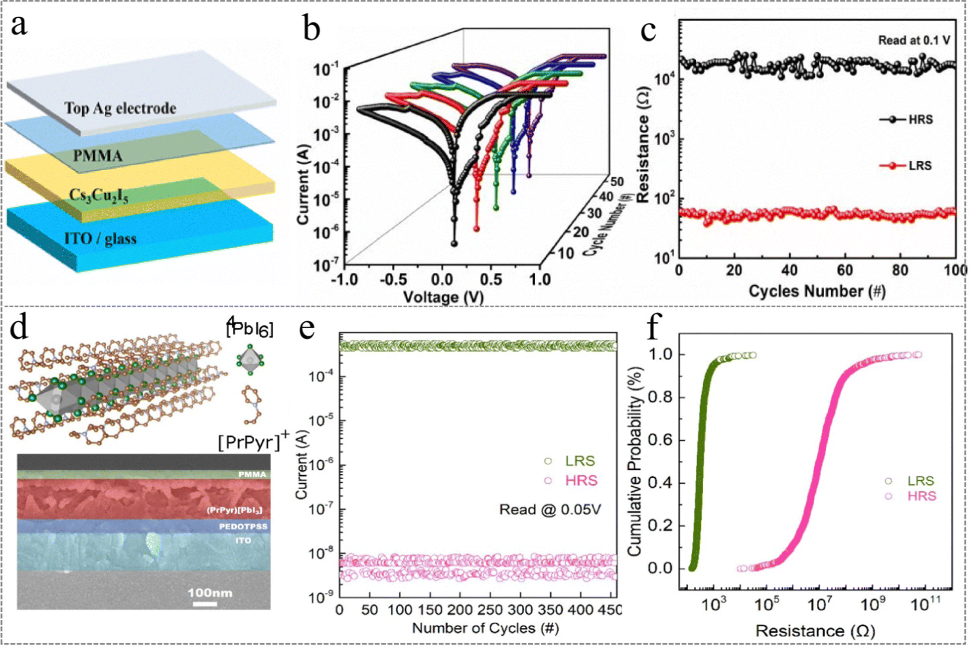 | ||
| Fig. 8 (a) Schematic of the memristor with the Ag/Cs3Cu2I5/ITO structure. (b) The I–V characteristic curves of the memristor over 50 sweeps. (c) The endurance test result of the Ag/PMMA/Cs3Cu2I5/ITO memristor at a read voltage of 0.1 V. Panels (a–c) are reproduced with permission.107 Copyright 2020, American Chemical Society. (d) The single-crystal structure of 1-D (PrPyr)[PbI3] and the SEM image of the memristive device. (e) Endurance test over 450 switching cycles at a read voltage of 0.05 V. (f) The cumulative probability distribution of the HRS and LRS via 1024 devices. Panels (d–f) are reproduced with permission.108 Copyright 2021, Nature Publishing Group. | ||
![[thin space (1/6-em)]](https://www.rsc.org/images/entities/char_2009.gif) 000 s). The proposed in situ technology can simplify the fabrication process and minimize the number of required stages. In 2021, a filamentary-type memristor with P-type selenium sulfide as the functional layer was prepared by Lu et al.112 This memristor used Ag and Pt as the electrode materials, and SnS was maintained in the thickness range of 10–40 nm, as seen in Fig. 9f. This device exhibited good resistive-switching performance, such as a low switching voltage of about 0.2 V, a fast switching speed of 1.5 ns (Fig. 9g), and an ultra-large on/off ratio of up to 108. A highly reproducible threshold-switching behavior between HRS and LRS over multiple cycles was observed via the I–V curves shown in Fig. 9h. The chip-scale simulations of memristors with a feature size of 50 nm and based on a high-density crossbar array showed a high learning accuracy of 87.76% for image classification, as shown in Fig. 9i.
000 s). The proposed in situ technology can simplify the fabrication process and minimize the number of required stages. In 2021, a filamentary-type memristor with P-type selenium sulfide as the functional layer was prepared by Lu et al.112 This memristor used Ag and Pt as the electrode materials, and SnS was maintained in the thickness range of 10–40 nm, as seen in Fig. 9f. This device exhibited good resistive-switching performance, such as a low switching voltage of about 0.2 V, a fast switching speed of 1.5 ns (Fig. 9g), and an ultra-large on/off ratio of up to 108. A highly reproducible threshold-switching behavior between HRS and LRS over multiple cycles was observed via the I–V curves shown in Fig. 9h. The chip-scale simulations of memristors with a feature size of 50 nm and based on a high-density crossbar array showed a high learning accuracy of 87.76% for image classification, as shown in Fig. 9i.
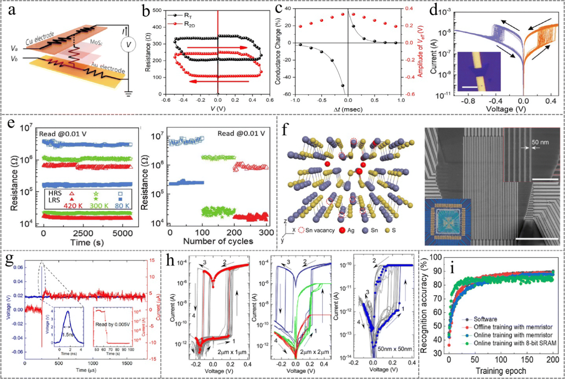 | ||
| Fig. 9 (a) The memristive device with the Au/MoS2 double layer/Au structure. (b) The measured resistance as a function of applied voltage. (c) The demonstration of STDP, the measured conductance of the memristive device and the effective voltage amplitude as a function of time. Panels (a–c) are reproduced with permission.109 Copyright 2019, American Chemical Society. (d) The I–V curve of the CuSe-based memristor during 100 cycles, and the inset shows an optical microscopic image of the CuSe-based memristor. (e) The retention performance test for LRS and HRS under a temperature gradient (left) and the endurance performance of the CuSe-based memristor (right). Panels (d–e) are reproduced with permission.110 Copyright 2022, Wiley-VCH. (f) The crystal structure of SnS and the SEM image of the memristor with a 32 × 32 high-density memristive crossbar array; the inset is an optical image of the chip. Scale bar, 1 μm. (g) The ultra-fast switching curve of the memristive device was read at a voltage of 0.02 V under a 4 V/1.5 ns voltage pulse. (h) The resistive switching behavior of the Ag/SnS/Pt memristor without current compliance (left) and with different current compliances (middle). The figure on the right exhibits the volatile resistive-switching feature of a device with the size of 50 nm × 50 nm. (i) The simulated classification accuracy results of the memristive device with the Ag/SnS/Pt structure for different images. Panels (f–i) are reproduced with permission.112 Copyright 2021, American Chemical Society. | ||
Different from the 2D material-based memristors made by the traditional mechanical stripping method, Liu et al. fabricated a memristive device with the Ti/HfSexOy/HfSe2/Au crossbar structure based on 2D HfSe2.113 This 2D memristive device exhibited excellent forming-free resistive-switching performance, including a fast switching speed (<50 ns), a low operating voltage of about 3 V, a large switching window (103), and outstanding data retention performance, as shown in Fig. 10a. Besides, a smaller operating current of 100 pA and a low power consumption of about 0.1 fJ were obtained with the Ti/HfSexOy/HfSe2/Au memristor (Fig. 10b), which are much lower than those of other Hf–O based memristors. To further improve performance, Li et al. demonstrated a practical method for implementing memristors based on polycrystalline HfSe2 thin films in neural network hardware.114 A low switching voltage of ∼0.6 V and a low switching energy of 0.82 pJ were demonstrated by the as-prepared device. When the switching cycle number exceeded 500, an endurance test with a resistance ratio of 100 was obtained, as shown in Fig. 10c. In addition, the simulation of synaptic weight plasticity was achieved using the as-prepared memristor device, and the simulation results of the artificial synapse under different pulse amplitudes are shown in Fig. 10d. In image recognition, the artificial neural network based on the 2D HfSe2 memristor demonstrated high accuracy (93.34%) and a narrow error distribution of 0.29% (Fig. 10e), achieving a high power efficiency of more than 8 trillion synapses per watt per second during operations. At present, the limited repeatability of the resistive-switching behavior and the high energy consumption of the memristor device greatly inhibit the application of synaptic devices in the field of neuromorphic computing. In 2021, Li et al. prepared a memristor based on a heterogeneous grain boundary using 2D PdSe2 as the functional layer.115 The resistive-switching behaviour of the Ti/PdSe2/Au memristor at different e-beam dosages is shown in Fig. 10f. This device exhibited anomalous resistive switching behavior in two fully interchangeable reset modes, as seen in Fig. 10g. The conductive mechanism of the device was local phase transition caused by electron beam irradiation, which formed an uneven grain boundary, and the formation of conductive filaments was induced by residual filaments along the grain boundary. Compared with the total-reset mode, the memristor exhibited increased switching change by 6 times when working in the quasi-reset mode (Fig. 10h), and it had a lower set voltage of about 0.6 V, long retention time, and a programmable multi-resistance state. The quasi-reset mode of the PdSe2-based memristor was applied in neuromorphic computing, realizing the simulation of synaptic plasticity and the implementation of the crossbar-array architecture under multimodal memory (Fig. 10i).
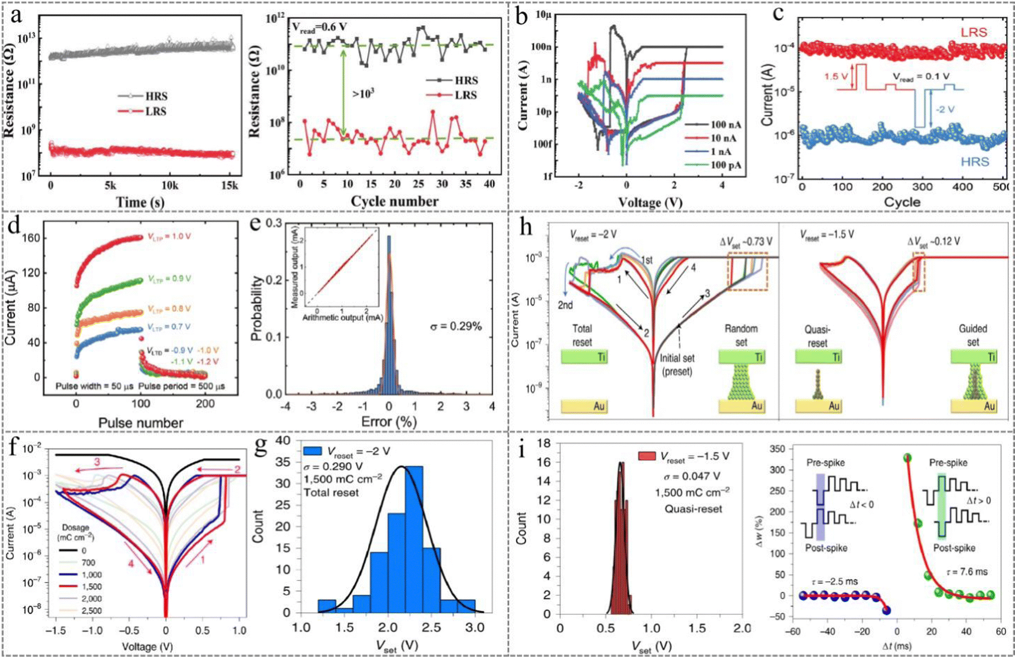 | ||
| Fig. 10 (a) The retention test of HRS and LRS at 0.1 V (left), and the measurement of HRS and LRS under 100 nA operation current at a read voltage of 0.6 V (right). (b) The nonvolatile resistive-switching behavior at different compliance currents (CC). Panels (a and b) are reproduced with permission.113 Copyright 2021, Wiley-VCH. (c) The endurance test over 500 cycles. (d) The LTP performance under positive/negative pulse training. (e) The corresponding error distribution between the measured results and the arithmetic results. Panels (c–e) are reproduced with permission.114 Copyright 2022, Wiley-VCH. (f) The resistive-switching behaviours of the Ti/PdSe2/Au memristive device under different e-beam dosages. (g) The interchangeable reset mode of the PdSe2 memristor under e-beam irradiation at −2 V. (h) The I–V curves of the PdSe2-based memristor during 100 cycles while operating in the total-reset mode (left) and the quasi-reset mode (right). (i) STDP simulation using the quasi-reset modes of the synaptic memristor. Panels (f-i) are reproduced with permission.115 Copyright 2021, Nature Publishing Group. | ||
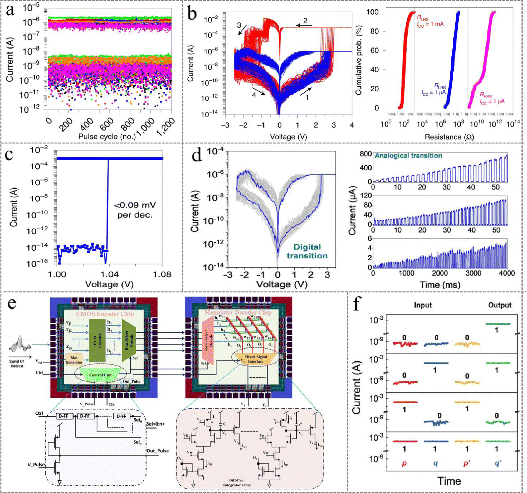 | ||
| Fig. 11 (a) The endurance test of the Au/Ag/h-BN/Au memristor over 1200 programming cycles. (b) The I–V characteristics measured over 120 cycles show the bipolar resistive-switching behavior of the h-BN memristor (left) and the cumulative distribution of HRS and LRS were measured over 1500 cycles (right). (c) The threshold-type resistive switching behaviour of the Ag/h-BN/Ag memristive device. The high ILRS/IHRS current window indicates excellent resistance recovery. Panels (a–c) are reproduced with permission.116 Copyright 2020, Nature Publishing Group. (d) The measured I–V characteristics exhibit nonvolatile bipolar resistive-switching behavior. (e) A comparison of the system architecture diagrams of the CMOS encoder chip and the memristor decoder chip. Panels (d and e) are reproduced with permission.117 Copyright 2022, Nature Publishing Group. (f) Logic implementation based on the Au/h-BN/Au memristor array for four input conditions. Panel f is reproduced with permission.118 Copyright 2022, Wiley-VCH. | ||
In addition, other types of ferroelectric materials have also been used to prepare nonvolatile memristors. In particular, with the investigation of ferroelectric materials, researchers are very interested in exploring next-generation nonvolatile ferroelectric memristors, which are expected to achieve high-density storage and arithmetic operations. Yan et al. fabricated a novel ferroelectric thin-film memristor with a BaTiO3-CeO2/La0.67Sr0.33MnO3/SrTiO3 vertically aligned nanocomposite structure on a monocrystalline Si substrate with SrTiO3 as the buffer layer.129 By improving the experimental conditions, vertically arranged epitaxial nanostructures were obtained, and the resistance characteristics were improved. Finally, the multi-value storage functions of these five states were obtained, and robust durability up to 109 cycles was observed. Moreover, the device successfully simulated the function of artificial synaptic paired-pulse facilitation. The algebraic computing capability at fast pulses with a width of about 50 ns was demonstrated. When applied for the recognition of datasets based on CNN, it achieved recognition rates of 90.03% and 92.55% for online and offline learning, respectively. In particular, the photoelectric synapse is also a novel type of artificial synapse combining optical pulse excitation and electrical pulse excitation, forming an important part of neuromorphic hardware development. Zhong et al. reported a double-stranded ferroelectric artificial synapse based on a photoelectric co-excited state,130 which used ultraviolet irradiation to generate excitatory postsynaptic currents and photoelectric dual controlled synapses. The memristor employed a training method based on ultraviolet excitation and ferroelectric enhancement, which greatly reduced the number of training pulses and increased synaptic plasticity. By using this memristor for the construction of convolutional neural networks, a 98.8% accuracy of data set recognition could be achieved.
Recently, Lin's group demonstrated improved characteristics of memristors with ferroelectric tunnel junctions (FTJs).131 In this work, a high-performance ferroelectric tunnel junction synapse based on the Ag/PZT/NSTO (Nb: 0.7 wt%) heterostructure was reported, in which (111)-oriented PbZr0.52Ti0.48O3 (PZT) is with an ultrathin thickness of ∼1.2 nm was designed and constructed. This device is close to the morphotropic phase boundary and exhibited multiple resistive switching and ultra-fine ferroelectric behaviors with ultra-high performance, including 256 states and 8-bit high-accuracy display (Fig. 12a), a sufficient conductance dynamic range (∼100×), remarkable endurance over 109 cycles (Fig. 12b), and ultra-low write power consumption. Fig. 12c shows the analog manipulation within the duration of ∼ 630 ps and a series of pulse voltages less than 5 V. The CNN simulated based on the device could achieve learning and image-recognition accuracy up to ∼94.7%, which is very close to the result of ∼95.6% obtained by the convolutional neural network software, as shown in Fig. 12d. In 2022, Gao et al. fabricated a novel three-terminal trihalide perovskite (MAPbI3) memristor with top-gate field effect geometry using the ferroelectric material poly-vinylidene fluoride-trifluoroethylene as the functional layer,132 as shown in Fig. 12e. Different working modes (volatilization and non-volatilization) could be created by modulating ion transport and the migration barrier at the switching interface of the non-filamentous perovskite memristor, which was able to simulate biological nociception for perceived pain and inhibited pain signals. Besides, the memristor could work in an environment with 7.8% cycle fluctuation and a current lower than 100 nA. The I–V curves of the memristor established over 100 cycles show analog switching characteristics with excellent cycle-to-cycle uniformity compared with a filament-based memristor, as shown in Fig. 12f. Recently, Cai et al. prepared a double-terminal ferroelectric synapse memristive device based on a disopropylammonium bromide/copper phthalocyanine heterostructure.133 The memristor utilized a copper phthalocyanine (CuPc) thin film (50 nm) as the semiconductor layer, and a high-quality disopropylammonium bromide thin film of thickness 500 nm was fabricated via a surface tension-assisted drop-casting method. The interfacial resistance was modulated by controlling the blocking effect of the polarization of the semiconductor, achieving synaptic features, including STDP, as shown in Fig. 12g. This optoelectronic synapse based on the ferroelectric/semiconductor interfacial memristor was applied in the construction of an ANN, which showed high image-recognition accuracy. Fig. 12h shows the variation in image-classification accuracy with noise between the weight quantification and unquantized models, and the structure and principle of the artificial neural-network-based image sensor are shown in Fig. 12i.
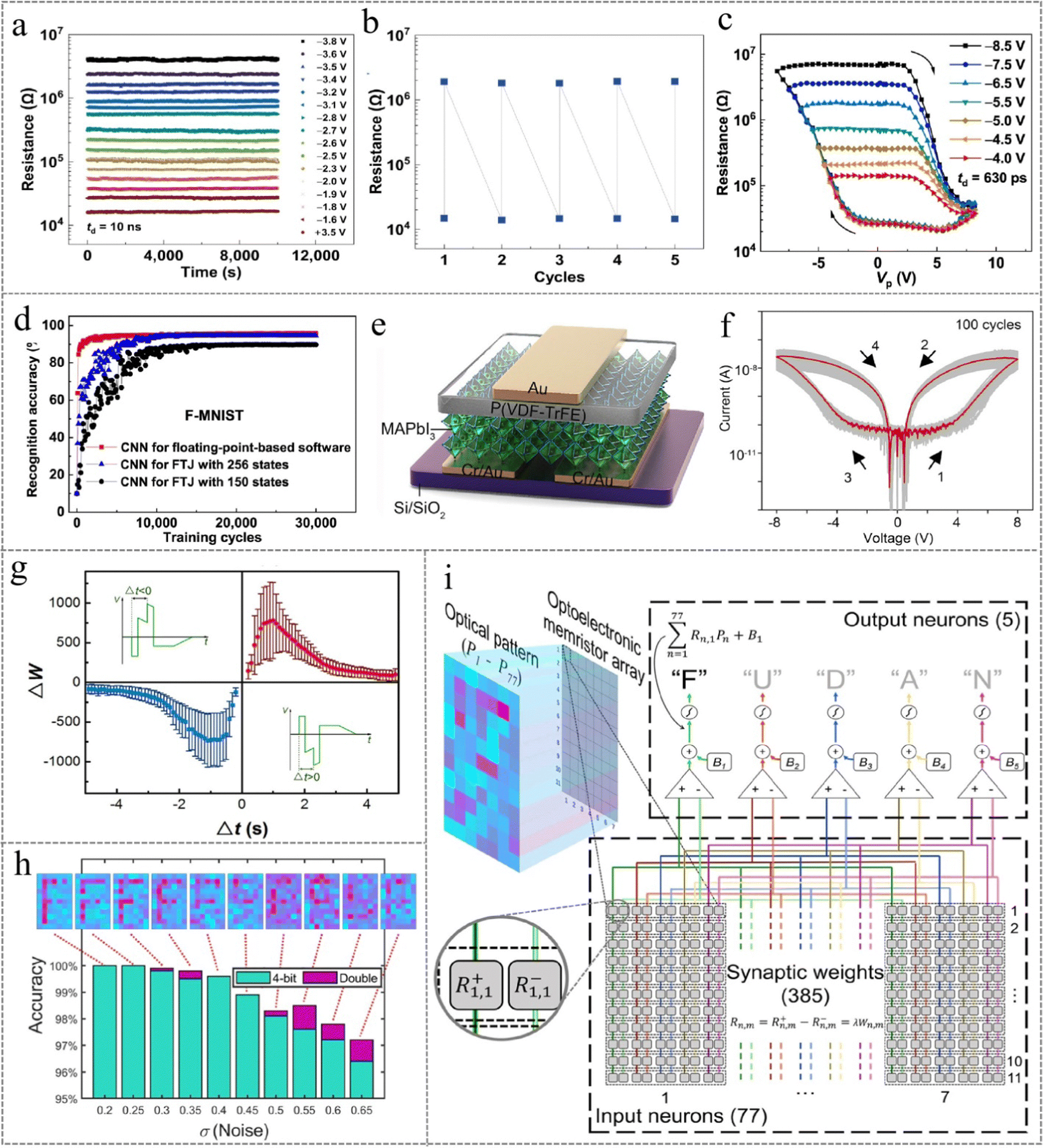 | ||
| Fig. 12 (a) The enhancement and suppression of 256 conductance states over 100 dynamic ranges by increasing a series of pulse voltages. (b) Five resistance-switching cycles of the ferroelectric tunnel junction with a (111)-oriented PbZr0.52Ti0.48O3 barrier after the 109 cycles. (c) The resistance measured at 0.05 V as a function of pulse voltage with a pulse duration of ∼630 ps. (d) The simulation results of the neural network based on different conductivity states and floating-point-based software learning. Panels (a–d) are reproduced with permission.131 Copyright 2022, Nature Publishing Group. (e) The schematic of the perovskite bimodal memristor. (f) The I–V curves measured based on the Au/MAPbI3/Au memristive device. Panels (e and f) are reproduced with permission.132 Copyright 2022, AIP Publishing. (g) The STDP simulation of the artificial synaptic devices. (h) The classification accuracy varies with noise; the green bars represent the accuracy after 4-bit weight quantization, and the purple bars represent the accuracy of the unquantized model. (i) The structure and principle of the artificial neural network image sensor. Panels (g–i) are reproduced with permission.133 Copyright 2022, Nature Publishing Group. | ||
Recently, some progress has been made in the application of ferroelectric memristors in neural networks. Wang et al. fabricated a three-terminal memristor with the Ag/WOx/BiFeOy/FTO structure by magnetron sputtering.134 This device showed favourable nonvolatile resistance-switching memory behavior, which meets the requirements for high-density information storage. Liu et al. demonstrated a BiFeO3 ferroelectric thin film of several-nanometer thickness for manipulating in-plane charged domain walls.135 The voltage control of the domain wall position in the BiFeO3 plane produced multiple nonvolatile resistance states in the W/SrRuO3/BiFeO3/SrRuO3/Nb–SrTiO3 ferroelectric memristor, thus realizing the key functional characteristics of a memristor with several unit-cell thickness. This promotes a better understanding of ferroelectric switches and provides a new strategy for creating unit-cell-scale devices. Besides, a memristor with the CeO2/Nb–SrTiO3 heterojunction structure136 exhibited a real-time conductance-tuning function with the application of a positive/negative pulse sequence. This memristor showed excellent conductance-switching behavior and a high switching ratio (105), further realizing the simulation of bio-synaptic functions. In addition, the CNN constructed using this memristor was used to identify the electrocardiogram data set, and the recognition accuracy was up to 93%, while the recognition accuracy for handwritten numbers reached 96%. Gao et al. proposed a three-terminal memristor with a top-gate field effect using a ferroelectric material, namely poly(vinylidene fluoride-trifluoroethylene), as the resistance layer.132 Two different operation modes (volatile and non-volatile) were realized by adjusting the ion transport and contact barrier at the switching interface of the ferroelectric memristor. In addition, the memristor showed ideal resistance-switching performance (high yield of 88.9%, cycle-to-cycle variation of 7.8%, and low operating current of less than 100nA). At the same time, this device realized the simulation of bio-nociception and blocked states.
2.2 Organic-memristor-based neural networks
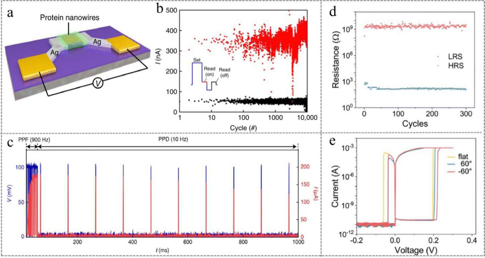 | ||
| Fig. 13 (a) The schematic of the memristive device with an Ag/protein nanowires/Ag structure. (b) The current of the vertical device at HRS and LRS over 104 cycles. (c) The conductance modulation of the protein-nanowire-based memristor. Panels (a–c) are reproduced with permission.138 Copyright 2020, Nature Publishing Group. (d) The endurance performance of the memristor. (e) The flexible performance of the device involving the resistive switching behavior of the memristor in the bent state. Panels (d and e) are reproduced with permission.139 Copyright 2021, Wiley-VCH. | ||
Biological systems are usually operated at a low voltage, but the operating voltage of traditional memristors is relatively high, which is not applicable to energy-saving biological systems. To address this issue, Zhao et al. demonstrated a high-performance filament-based threshold-switching (TS) memristor, which exhibited an on-current of 1 mA, a low threshold voltage of 0.17 V, and high selectivity of 3 × 106.38 In addition, this memristive device showed excellent uniformity and stability, demonstrating typical bio-synaptic STP, including facilitation to the pulse, even at high humidity (80%) and a high temperature (70 °C).
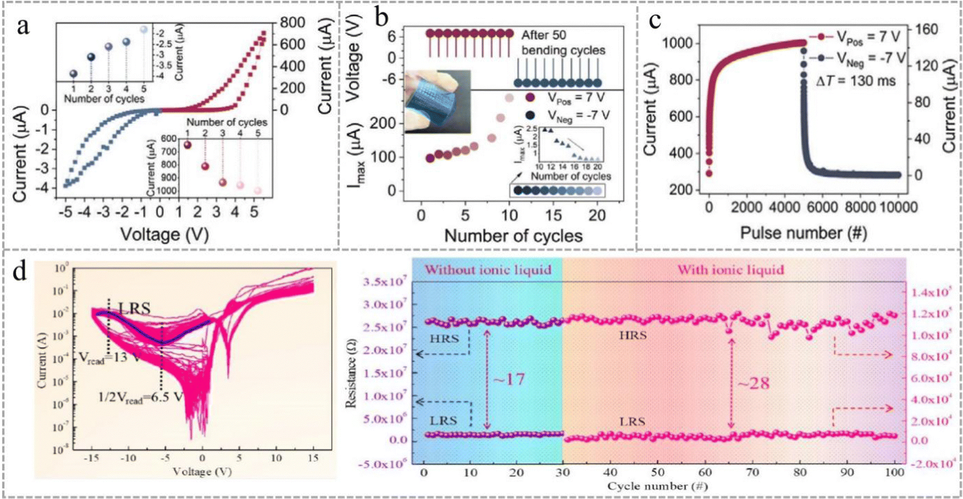
In addition to using proteins as the functional layer material in memristor devices, many studies have also used sugars for the preparation of memristors. Min et al. reported a memristor prepared using the biomaterial chitosan-based solid polymer electrolyte (SPE).141 They used the SPE-chitosan as the functional layer of the double-terminal memristive device with a Ti/SPE-chitosan/Pt structure. Due to the electrochemical reactions between the electrolyte and metal ions, this device exhibited stable bipolar resistive-switching behavior with excellent durability for 500 cycles. The I–V characteristics of multilevels per cell with bipolar resistive switching were also achieved by adjusting the SET current, and the STP and LTP of bio-synapses were also simulated. In 2021, a wafer-grade acid polysaccharide thin film with significant transient properties has been reported as a promising memristive material.142 This memristor is independent, lightweight, and could be completely dissolved in deionized water within 3.5 s. The ion-constraining ability of the acid polysaccharides allowed the cations to interact with ionizable acid groups, thus enabling atomic manipulation. It has been reported that the individual device could generate 16 highly controllable and mutually independent quantized conductance (QC) states with nonvolatile properties, and QC switching could be performed at an ultra-fast speed of 2–5 ns with a low energy consumption of 0.6–16 pJ. Furthermore, the encoding/decoding and nonvolatile fundamental Boolean logic were designed and implemented as they are important for developing nanodevices with quantum effects. Zhang's group developed a chitosan (CS)-prototype graphene oxide (rGO) interpenetration network electrolyte and applied it as the functional layer of a memristive device to develop a reproducible low-power polymorphic biomemristor.143 The designed cross-through network structure enhanced the stability of the device and improved the ionic conductivity. The biomemristor showed stable bipolar resistance-switching behavior with good stability, reproducible polymorphic storage, and low programming power of 9.4 μW. Moreover, this device presented good biocompatibility and excellent deformation stability during 1000 bending cycles, confirming the possibility of the application of this high-performance biomemristor in artificial sensing systems.
Using natural biomaterials in the functional layer to manufacture electronic devices meets the requirements of sustainable green electronics and is also suitable for preparing biomemristors. Li's group demonstrated an organic memory synapse formed using dichloropalphthalocyanine, which was capable of switching conversion under the temperature of 300 °C,144 as shown in Fig. 14a. In addition, the flexible device maintained stable resistance switching behavior after 50 consecutive mechanical bending cycles, as shown in Fig. 14b. Fig. 14c shows that the device could simulate a trainable and reconfigurable memristor array and perform image information processing. This finding provides a reference for the application of thermoelastic organic synaptic devices in neuromorphic computing. Recently, anthocyanin (C15H11O6), a sustainable natural biomaterial, was used for ion and electron transport.39 It could significantly modulate the capacitive-coupled memristive behavior of the as-prepared biomemristor. By inserting graphene into the biomaterial matrix, memory effect manipulation through graphene protonation was achieved. Finally, this device was applied to the 0T-1R array configuration, demonstrating the potential application of battery-like self-selected biomemristors in brain-inspired neuromorphic computing, data storage systems, and high-density device integration, as shown in Fig. 14d.
 | ||
| Fig. 14 (a) The I–V characteristics under positive and negative voltage sweeps before the cyclic bending test. (b) The change in current acts as a function of cycle number; the inset on the right indicates the change in current versus the number of sweep cycles under negative bias. (c) Current change under the continuous stimuli of 7 V/−7 V pulses corresponding to potentiation and depression, respectively. Panels (a–c) are reproduced with permission.144 Copyright 2021, Wiley-VCH. (d) The cyclic test of HRS/LRS and the I–V nonlinear performance of the Mo/C15H11O6-graphene/Mo device with an ionic liquid. Panel d is reproduced with permission.39 Copyright 2021, American Chemical Society. | ||
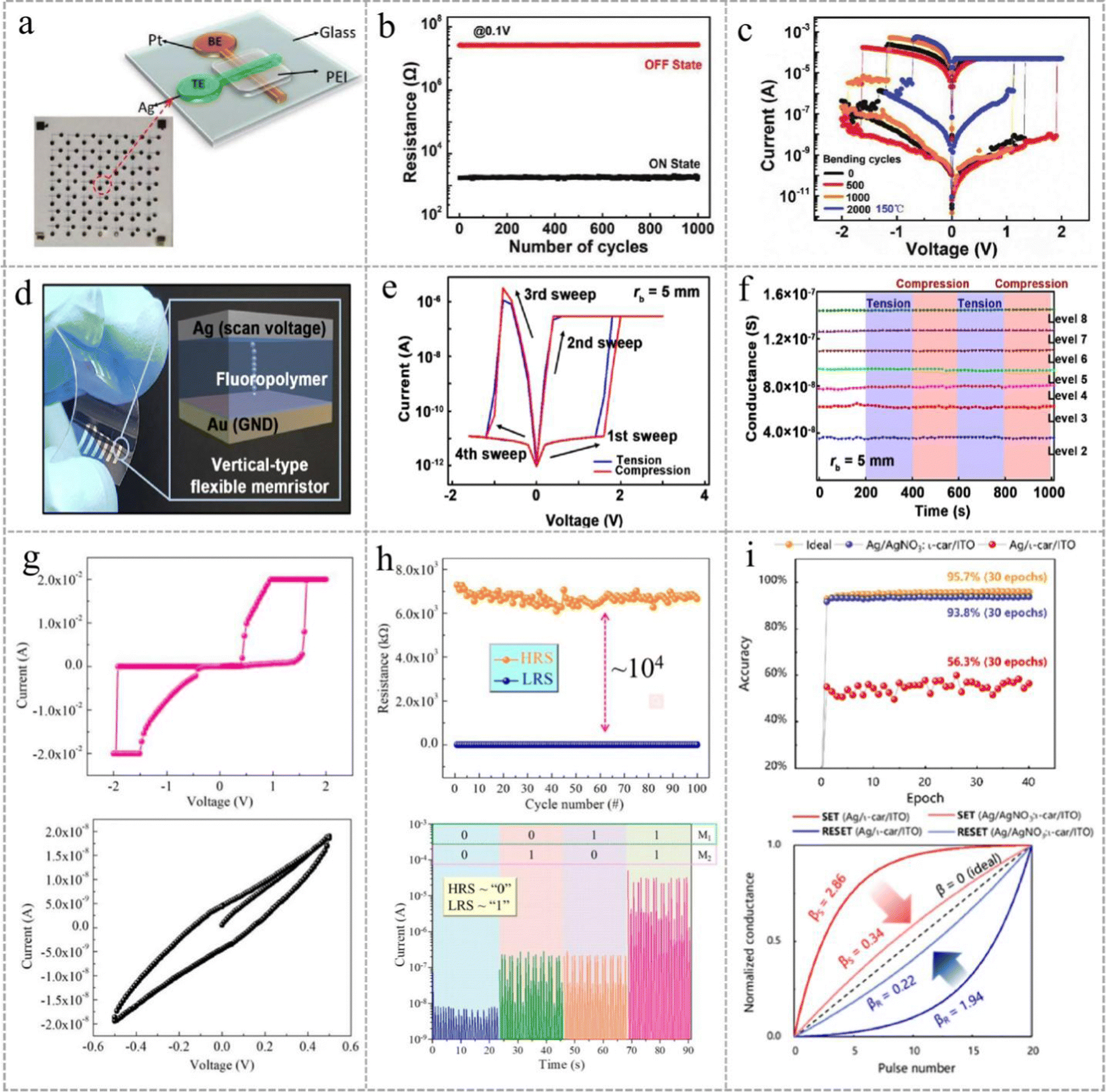 | ||
| Fig. 15 (a) The schematic of the Ag/PEI/Pt memristive device. (b) The cycle performance of the memristive device at HRS and LRS during 1000 cycles at 0.1 V. (c) The I–V curves of the Ag/PEI/Pt/PI memristive device under repeated mechanical bending for 2000 times. Panels (a–c) are reproduced with permission.145 Copyright 2020, Wiley-VCH. (d) The photographic image and device structure of the fluoro-polymer-based flexible memristor under bending deformation. (e) The I−V characteristics of the memristive device under bending stresses with a radius of 5 mm. (f) The reliable multilevel memory properties expressed via artificial synapses and its electromechanical stability at seven memory states. Panels (d–f) are reproduced with permission.146 Copyright 2021, Nature Publishing Group. (g) The I–V characteristics of the memristive device at different voltages (0.5 V top, 1 V bottom). (h) The endurance test of the high/low resistance states and the logical operation of the Ag/AZB:PMMA/FTO memristive device at a read voltage of 0.25 V. Panels (g and h) are reproduced with permission.147 Copyright 2022, American Chemical Society. (i) A comparison of the linearity of the weight update curves (bottom) and the recognition accuracy of the handwritten digits (top). Panel i is reproduced with permission.148 Copyright 2021, American Chemical Society. | ||
2.3 Challenges and strategies for memristor-based neural networks
At present, a series of progress has been made in the hardware implementation of mathematical models based on synapses, neurons and neural networks. The realization of artificial neural networks on chips mainly depends on the memristor, and the application of memristor dynamics in neural networks has achieved great development, such as first-order memristors, second-order memristors and dynamic memristors.150 Among them, first-order memristors provide a wide variety and account for the majority; they can show continuous resistance changes when different amplitude voltage pulses are applied.151 At present, some synaptic learning functions, such as STP, LTP and STDP, have been successfully demonstrated in these electronic synapses.152,153 However, the modulation of first-order memristor conductance is only controlled by the applied external voltage, which results in some synaptic characteristics (such as the shape of presynaptic and postsynaptic voltage pulses) being not well simulated. Second-order memristors can simulate the time dynamics of bio-synapses through the ion drift and diffusion dynamics of metal species. In a second-order memristor, the conductivity is controlled by some internal time mechanisms, and the relative timing information is captured by the second-state variables (thermal dissipation of oxygen vacancies in the conducting filament,154 the decay of oxygen vacancy mobility,155 the minimization of interfacial energy of the metal species,156 and so on). Its activation and spontaneous decay following external spike stimuli provide an internal mechanism to encode the temporal spike information and thus enable natural modeling of the frequency responses. Currently, most second-order memristor devices can be used to simulate temporal synaptic performance on the chip. However, there are some significant obstacles to connecting neural networks with memristors, especially in situations where the stability of the device is critical to computational accuracy. In the process of conductance modulation, the memristor will demonstrate atomic-scale random defects and variations, among which uncontrolled ion migration in the memristor device has a great influence on the device-to-device and cycle-to-cycle variation, cycling endurance and dynamic range (on/off ratio). The uncertain drifts in the conductance state over time or environment change correlate with undesired changes in synaptic weight in neural networks. The emergence of non-ideal memristor characteristics has become the main factor that affects the learning accuracy of neural networks, and it has always been one of the main challenges faced by neural network-based systems.157 Besides, the reliability concepts and material characterization methods for analog memristors vary widely, and generally accepted evaluation criteria are still lacking. At the same time, the complexity of the physical mechanism of analog resistive switching makes it difficult to study the mechanism of device reliability. This makes the cross-layer co-design from device to system/algorithm incomplete, thereby also restricting the application of memristors in neural networks.In order to improve the application of memristors in neural networks, researchers have tried to provide some feasible solutions from the aspects of process technology, innovative materials, the structure of the memristor and the programming scheme. Some methods have been proposed to reduce the retention loss, enhance retention and improve the on/off ratio by adding annealing operation and metal doping.158,159 Recently, some researchers have also focused on improving the memristive properties of memristors. Sung et al. proposed a capacitance-dependent voltage division analysis to suppress the hidden current generated by adjacent units in a 3D memristive array.160 This method effectively reduced the leakage of the interface capture current between the resistive switching and metal layers, resulting in excellent retention (>5 × 10⁵). Liu et al. synthesized wafer-scale ultrathin 2D imine polymer films with controllable thickness using the Schiff base polycondensation reaction method, thus improving the preparation method of memristors.161 This free-standing porous film exhibited a feasible switching performance (endurance and data retention up to 200 cycles and 8 × 10⁴ s, respectively). Yin et al. successfully realized current limitations by controlling the space charge in a 2D-Bi2Se3-based memristor using a damage-less ion implantation technology by using ultra-low energy plasma.162 The memristors exhibited stable resistive switching behavior, including a high resistive switching ratio of 104, excellent cycle durability up to 300 cycles, and excellent retention (>104 s). Recently, Kim et al. proposed a new material stacking method in order to improve the switching performance of memristors.163 A memristive cross-array stack with the Pt/Ta2O5/Nb2O5−x/Al2O3−y/Ti structure exhibited a high retention characteristic (retention time over 105 s at 150 °C). Su et al. designed a new multilevel nonvolatile lead-free cesium halide memristor with lead-free cesium halide in the MoOx interface layer as the functional layer, and a highly uniform and reproducible memristor was obtained.164 This device showed a long retention time (>106 s), high durability (>105), and an ultra-high on/off ratio of 1010. Towards the improvement of the preparation method, Tang et al. demonstrated a solution-treated 2D-MoS2 memristor array and realized 3D integration by stacking 2D-MoS2.165 This memristor could adjust the switching characteristics through the diffusion of sulfur vacancies between the thin sheets, resulting in excellent durability, long memory retention, low device difference, high analog on/off ratio and linear conductance update. Generally, there are two main research directions to improve the performance of memristors at the material level. One is to explore growth conditions and modification processes to improve the physical properties and interface quality of the memristive materials, and the other is to explore new materials with unique properties through experiments, software simulation and machine learning.24,166
3. Summary and Outlook
Since 2010, the integration of crossbar arrays and memristors has been attempted to implement hardware neuromorphic computing.153 The large-scale and high-density neural network integration of memristor devices is crucial for logic computing, but most of the neural networks fabricated so far do not meet the theoretical requirements. In other words, the neural networks can imitate the bio-synaptic function of the human brain to a certain extent, but the integrated array size is still not large enough, and the integration density is not high enough, thus hindering the practical application of memristor-based neural networks. There are two main reasons for the difficulties in the large-scale integration of memristors. One is that the integration of large-scale memristor devices into the crossbar array to form a high-density memristor matrix can increase the parasitic line resistance of the crossbar array, thus greatly reducing the calculation accuracy of the memristor-based neural networks. On the other hand, the integrated crossbar array of the memristors may have a problem in interaction, which makes programming very difficult. In addition, the variations in material design and process methods involved in the process of manufacturing memristive devices further affect performance uniformity and the stability of the memristor arrays.At present, although some 2D materials with high crystallinity can be fabricated via exfoliation techniques, it is still challenging to prepare 2D materials with large areas and uniform physical properties. The synthesis methods and transfer techniques for industrial-scale production still need to be improved for large-area and high-quality 2D materials. Most 2D semiconductors easily react or oxidize under ambient conditions, resulting in the degradation of device performance. For some other memristors, such as the Hewlett-Packard memristor, although several mechanisms have been proposed to explain the behavior of the memristor; however, the exact explanation is not uniform enough, and the underlying cause of the memristive effect has not yet been completely discovered. Therefore, finding a reliable and in-depth theory to understand and optimize the memristive effect has become an urgent issue. In addition, the compatibility of the memristors with existing CMOS fabrication processes has also become another limiting factor for the development of memristor-based brain-like chips. Therefore, more efforts are needed in material design, nanostructure manipulation, film homogeneity, stability, and fundamental physical properties in order to further develop the application of memristor-based neural networks in artificial intelligence.
One of the ways to solve the integration challenge is to use three-dimensional (3D) stacked memory devices to reduce the parasitic line resistance of each individual layer. Since cognitive operations in high-dimensional spaces rely on a large number of weights, they naturally require high memory density. Therefore, 3D vertical stacking of memory beams may be advantageous in terms of integrated density per unit area. The summary and comparison of some representative memristors based on different materials are shown in Table 1. It is believed that the variability problem can be solved by reducing the memory unit size, for example, the most advanced memory feature size is about 10 nm. In addition, the change in the resistive switching characteristics of the memristive device is related to the randomness of the conductive filament in the formation process. Theoretically, this can be avoided when the size of the memristor is reduced to the atomic level. In practice, if the size of the memristor is further reduced, it is possible to limit the filament to a smaller volume so as to better adjust the number and shape of the filaments. It should be considered that a single conductive filament comparable to the device size not only improves the uniformity of device performance, but also reduces the size of the memristive device, which eventually reduces the programming current requirement of the memristor unit, thereby significantly reducing power consumption.
| Devices | Thickness of functional layer (nm) | On/off resistance ratio | Retention time (s) | Endurance (cycles) | Ref. |
|---|---|---|---|---|---|
| Pt/h-BN/Ag | 0.33 | 107 | N | 108 | 95 |
| Ag/PMMA/Cs3Cu2I5/ITO | 500 | 102 | 104 | 100 | 107 |
| Ag/CsPbBr3 NCs/PTPO/PEDOT:PSS/ITO | 70 | 103 | 105 | 5655 | 167 |
| Ti/PdSe2/Au | 3 | 103 | 105 | 100 | 115 |
| Cr/CuSe/Au | 2.4 | 100 | 106 | 300 | 110 |
| Ag/HfOx/Pt | 300 | 103 | 104 | 100 | 168 |
| Ag/CuInSe2/Mo | 400 | 4 × 10⁵ | 104 | 160 | 169 |
| Ag/Ag2S/Ag | 100 | 102 | 104 | 105 | 170 |
| Ag/STO:Ag/SiO2/p++-Si | 70 | 103 | 104 | 103 | 16 |
| Ag/CeO2/Pt | 27 | 4 | 5 × 10⁴ | 100 | 171 |
| Ta/Ta2O5/ZrO2/Pt | 12 | 102 | 104 | 104 | 172 |
| Al/polymer membrane/ITO | 300 | 103 | 104 | 20 | 173 |
| Al/hollow MEH-PPV/2D CMP/ITO | 45 | 105 | 3 × 10⁴ | 50 | 174 |
| Ag/CS-rGO/ITO/PET | 80 | 103 | 104 | 100 | 143 |
| Ag/fluoropolymer/Au | 280 | 105 | 2000 | 400 | 146 |
| Ag/PEI/Pt | 400 | 105 | 105 | 1000 | 145 |
Memristor-based artificial neural networks are discussed in terms of materials, device structure, operating mechanism, and application scope. As shown in Fig. 16, since the discovery of memristive materials, a great variety of materials have been used for the fabrication of memristive devices ranging from inorganic materials, organic materials, and inorganic-organic hybrid materials. The memristors based on inorganic materials are covered with traditional oxide materials, insulating hexagonal BN, transition metal sulfides, 2D-MXenes materials, ferroelectric materials, etc. Organic materials, including natural materials such as proteins, carbohydrates, DNA, fibers, and organic polymers, have also been applied for the preparation of memristive devices.175 An extensive range of materials, including 0-dimensional, 1-dimensional, 2-dimensional and 3-dimensional materials, have been employed. At present, the major route to developing memristive materials is to improve material synthesis methods and broaden the material systems.176–180 This is mainly reflected in optimizing the preparation and growth of materials. On the other hand, it is necessary to continuously improve the interface effect of materials and conduct more in-depth research on the special properties of materials in different dimensions. Furthermore, at the network construction level, it is essential to continuously optimize the algorithm hardware design to improve the integration density of the memristive devices and the stability between memristors.
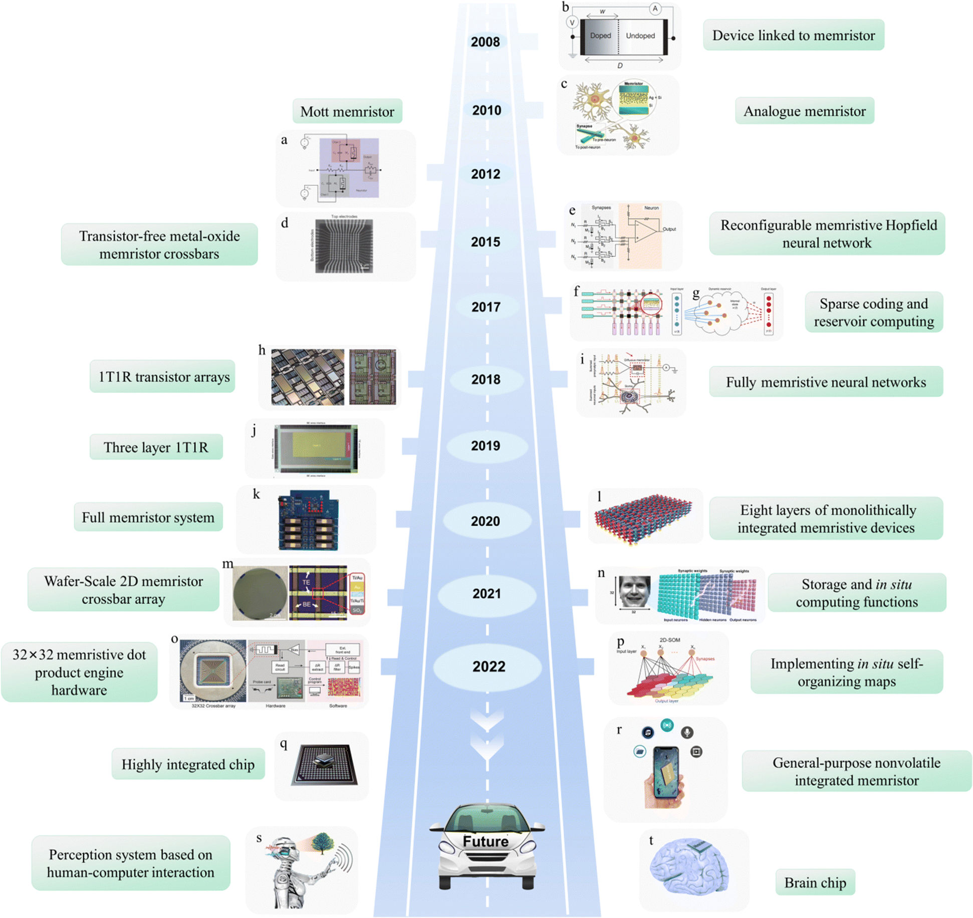 | ||
| Fig. 16 The development roadmap and future work trend for memristor-based neural networks for neuromorphic computing and artificial intelligence applications. (a) Mott memristor. Panel a is reproduced with permission.181 Copyright 2012, Nature Publishing Group. (b) A device linked to the memristor. Panel b is reproduced with permission.2 Copyright 2008, Nature Publishing Group. (c) An analogue memristor. Panel c is reproduced with permission.153 Copyright 2010, American Chemical Society. (d) An integrated 12 × 12 crossbar. Panel d is reproduced with permission.182 Copyright 2015, Nature Publishing Group. (e) A reconfigurable memristive Hopfield neural network. Panel e is reproduced with permission.183 Copyright 2015, Nature Publishing Group. (f) Sparse coding. Panel f is reproduced with permission.184 Copyright 2017, Nature Publishing Group. (g) Reservoir computing. Panel g is reproduced with permission.185 Copyright 2017, Nature Publishing Group. (h) A 1T1R transistor array. Panel h is reproduced with permission.186 Copyright 2018, Nature Publishing Group. (i) Fully memristive neural networks. Panel i is reproduced with permission.187 Copyright 2018, Nature publishing Group. (j) A three-layer 1T1R. Panel j is reproduced with permission.188 Copyright 2019, Nature Publishing Group. (k) A full memristor system. Panel k is reproduced with permission.85 Copyright 2020, Nature Publishing Group. (l) The eight layers of monolithically integrated memristive devices. Panel l is reproduced with permission.189 Copyright 2020, Nature Publishing Group. (m) A wafer-scale 2D memristor crossbar array. Panel m is reproduced with permission.114 Copyright 2022, Wiley-VCH. (n) Storage and in situ computing functions. Panel n is reproduced with permission.86 Copyright 2021, Elsevier. (o) A 32 × 32 crossbar array. Panel o is reproduced with permission.87 Copyright 2022, Wiley-VCH. (p) Implementing in situ self-organizing maps. Panel p is reproduced with permission.190 Copyright 2022, Nature Publishing Group. (q) A highly integrated chip. (r) A general-purpose nonvolatile integrated memristor. (s) A perception system based on human-computer interaction. (t) A brain chip. | ||
In summary, we have reviewed in detail the technologies relevant to the integration of neural networks based on memristors, from the materials used for preparing memristors and various advanced applications of neural networks to the future prospects of artificial intelligence. At the same time, the types of functional materials commonly used in memristors and their working mechanisms are analyzed comprehensively. In particular, the important characteristics of 2D materials and ferroelectric materials used to fabricate memristive devices and the mechanisms of the polymorphic memory phenomena in resistive-switching devices are summarized. In addition, this review also discusses the development status, basic operating principles and key challenges of the latest technology and the application of memristor-based neural networks in neuromorphic computing. Furthermore, some scalable applications based on memristive neural networks, including memory computing, logic computing and logic display, are also discussed. Therefore, this review systematically summarizes the extensive research on neural networks based on memristors to achieve the application of optimized memristors and more energy-efficient neuromorphic computing systems for advanced artificial intelligence.
Conflicts of interest
The authors declare no competing financial interest.Acknowledgements
The authors gratefully acknowledge financial support from the Fundamental Research Funds for the Central Universities (Grant No. 2682021CX076), the National Key R&D Program of China (No. 2017YFE0301401), and B. Sun is grateful to the Xi’an Jiaotong University for the financial support of the young talent project.References
- L. Chua, IEEE Trans. Circuit Theory, 1971, 18, 507–519 Search PubMed.
- D. B. Strukov, G. S. Snider, D. R. Stewart and R. S. Williams, Nature, 2008, 453, 80–83 CrossRef CAS PubMed.
- P. Hou, J. Wang, X. Zhong and Y. Wu, RSC Adv., 2016, 6, 54113–54118 RSC.
- H. Yildirim and R. Pachter, ACS Appl. Electron. Mater., 2019, 1, 467–477 CrossRef CAS.
- C. Hsu, Y. Wang, C. Wan, I. Wang, C. Chou, W. Lai, Y. Lee and T. Hou, Nat. Nanotechnol., 2014, 25, 165202 CrossRef PubMed.
- R. Waser and M. Aono, Nat. Mater., 2007, 6, 833–840 CrossRef CAS PubMed.
- M. K. Akbari and S. Zhuiykov, Nat. Commun., 2019, 10, 3873 CrossRef PubMed.
- M. Kumar, H. S. Kim and J. Kim, Adv. Mater., 2019, 31, 1900021 CrossRef PubMed.
- Y. Ren, L. Hu, J.-Y. Mao, J. Yuan, Y.-J. Zeng, S. Ruan, J.-Q. Yang, L. Zhou, Y. Zhou and S.-T. Han, J. Mater. Chem. C, 2018, 6, 9383–9393 RSC.
- L. Fan, Y. Chen, Q. Liu, S. Chen, L. Zhu, Q. Meng, B. Wang, Q. Zhang, H. Ren and C. Zou, ACS Appl. Mater. Interfaces, 2016, 8, 32971–32977 CrossRef CAS PubMed.
- K. Liu, L. Qin, X. Zhang, J. Zhu, X. Sun, K. Yang, Y. Cai, Y. Yang and R. Huang, Faraday Discuss., 2019, 213, 41–52 RSC.
- Y. Yang, X. Zhang, L. Qin, Q. Zeng., X. Qin and R. Huang, Nat. Commun., 2017, 8, 15173 CrossRef PubMed.
- Z. Shen, Y. Qi, I. Z. Mitrovic, C. Zhao, S. Hall, L. Yang, T. Luo, Y. Huang and C. Zhao, Micromachines, 2019, 10, 446 CrossRef PubMed.
- Y. Goh and S. Jeon, Nanotechnology, 2018, 29, 335201 CrossRef PubMed.
- Z. Xiao and J. Huang, Adv. Electron. Mater., 2016, 2, 1600100 CrossRef.
- N. Ilyas, J. Wang, C. Li, H. Fu, D. Li, X. Jiang, D. Gu, Y. Jiang and W. Li, J. Mater. Sci. Technol., 2022, 97, 254–263 CrossRef.
- C. Papakonstantinopoulos, P. Bousoulas, M. Tsigkourakos, D. Sakellaropoulos, L. Sygellou and D. Tsoukalas, ACS Appl. Nano Mater., 2021, 3, 2729–2737 CAS.
- P. Bousoulas, D. Sakellaropoulos and D. Tsoukalas, Appl. Phys. Lett., 2021, 118, 143502 CrossRef CAS.
- Y. X. Yu, L. Pan, M.-K. Son, M. L. Mayer, W.-D. Zhang, A. Hagfeldt, J. Luo and M. Grätzel, ACS Energy Lett., 2018, 3, 760–766 CrossRef CAS.
- J. Bera, A. Betal, A. Sharma, U. Shankar, A. K. Rath and S. Sahu, ACS Appl. Nano Mater., 2022, 5, 8502–8510 CrossRef CAS.
- X. Zhao, H. Xu, Z. Wang, Y. Li and Y. Liu, InfoMat, 2019, 1, 183–210 CrossRef CAS.
- M. K. Mojadidi, P. Kumar, A. N. Mahmoud, I. Y. Elgendy, H. Shapiro, B. West, A. C. Charles, H. P. Mattle, S. Sorensen, B. Meier, S. D. Silberstein and J. M. Tobis, J. Am. Coll. Cardiol., 2021, 77, 667–676 CrossRef PubMed.
- S. Ren, L. Tang, Q. Sun, Z. Li, H. Yang and W. Chen, J. Alloys Compd., 2018, 763, 638–642 CrossRef CAS.
- S. Anwarhussaini, H. Battula, P. K. R. Boppidi, S. Kundu, C. Chakraborty and S. Jayanty, Org. Electron., 2020, 76, 105457 CrossRef.
- C.-H. Hsu, J.-S. Lin, Y.-D. He, S.-F. Yang, P.-C. Yang and W. S. Chen, Thin Solid Films, 2011, 519, 5033–5037 CrossRef CAS.
- J. Xiao, W. L. Ong, Z. Guo, G. W. Ho and K. Zeng, ACS Appl. Mater. Interfaces, 2015, 7, 11412–11422 CrossRef CAS.
- C. Li, C. E. Graves, X. Sheng, D. Miller, M. Foltin, G. Pedretti and J. P. Strachan, Nat. Commun., 2020, 11, 1638 CrossRef.
- Q. Cao, W. Lü, X. R. Wang, X. Guan, L. Wang, X. Guan, L. Wang, S. Yan, T. Wu and X. Wang, ACS Appl. Mater. Interfaces, 2020, 12, 42449–42471 Search PubMed.
- L. Minati, L. V. Gambuzza, W. J. Thio, J. C. Sprott and M. Frasca, Chaos Soliton. Fract., 2020, 138, 109990 CrossRef.
- L. Sun, Z. Wang, J. Jiang, Y. Kim, B. Joo, S. Zheng, S. Lee, W. J. Yu, B. S. Kong and H. Yang, Sci. Adv., 2021, 7, eabg1455 CrossRef CAS PubMed.
- W. Yao, C. Wang, Y. Sun, C. Zhou and H. Lin, App. Math. Comput., 2020, 386, 125483 CrossRef.
- S. Pi, C. Li, H. Jiang, W. Xia, H. Xin, J. J. Yang and Q. Xia, Nat. Nanotechnol., 2019, 14, 35–39 CrossRef CAS PubMed.
- Z. Wang, M. Rao, R. Midya, S. Joshi, H. Jiang, P. Lin, W. Song, S. Asapu, Y. Zhuo, C. Li, H. Wu, Q. Xia and J. J. Yang, Adv. Funct. Mater., 2018, 28, 1704862 CrossRef.
- S. Yu, B. Gao, Z. Fang, H. Yu, J. Kang and H.-S. P. Wong, Adv.Mater., 2013, 25, 1774–1779 CrossRef CAS PubMed.
- L. Cheng, Y. Li, K.-S. Yin, S.-Y. Hu, Y.-T. Su, M.-M. Jin, Z.-R. Wang, T.-C. Chang and X.-S. Miao, Adv. Funct. Mater., 2019, 29, 1905660 CrossRef CAS.
- W. Zhang, B. Gao, J. Tang, P. Yao, S. Yu, M.-F. Chang, H.-J. Yoo, H. Qian and H. Wu, Nat. Electron., 2020, 3, 371–382 CrossRef.
- K. Wang, J. Chen and X. Yan, Nano Energy, 2021, 79, 105453 CrossRef CAS.
- M. Zhao, S. Wang, D. Li, R. Wang, F. Li, M. Wu, K. Liang, H. Ren, X. Zheng, C. Guo, X. Ma, B. Zhu, H. Wang and Y. Hao, Adv. Electron. Mater., 2022, 8, 2101139 CrossRef CAS.
- B. Sun, T. Guo, G. Zhou, J. Wu, Y. Chen, Y. N. Zhou and Y. A. Wu, ACS Appl. Bio. Mater., 2021, 4, 1976–1985 CrossRef CAS PubMed.
- D. Ielmini and G. Pedretti, Adv. Intell. Syst., 2020, 2, 2000040 CrossRef.
- S. Seo, J.-H. Lee, R.-G. Lee, T.-H. Kim, S. Park, S. Jung, H.-K. Lee, M. Andreev, K.-B. Lee, K.-S. Jung, S. Oh, H.-J. Lee, K. S. Kim, G. Y. Yeom, Y.-H. Kim and J.-H. Park, Adv. Mater., 2021, 33, e2102980 CrossRef PubMed.
- S. Oh, J.-H. Lee, S. Seo, H. Choo, D. Lee, J.-I. Cho and J.-H. Park, Adv. Sci., 2022, 9, e2103808 CrossRef PubMed.
- P. Pfeiffer, I. L. Egusquiza, M. D. Ventra, M. Sanz and E. Solano, Sci. Rep., 2016, 426, 29507 CrossRef PubMed.
- S. Mao, X. Zhang, G. Zhou, Y. Chen, C. Ke, W. Zhou, B. Sun and Y. Zhao, ACS Appl. Electron. Mater., 2021, 3, 5537–5547 CrossRef CAS.
- M. Spagnolo, J. Morris, S. Piacentini, M. Antesberger, F. Massa, A. Crespi, F. Ceccarelli, R. Osellame and P. Walther, Nat. Photonics, 2022, 16, 318–323 CrossRef CAS.
- S. Oh, H. Hwang and I. K. Yoo, APL Mater., 2019, 7, 091109 CrossRef.
- S. Yu, Proc. IEEE, 2018, 106, 260–285 CAS.
- D. Silver, A. Huang and C. J. Maddison, et al. , Nature, 2016, 529, 484–489 CrossRef CAS PubMed.
- D. S. Jeong, K. M. Kim, S. Kim, B. J. Choi and C. S. Hwang, Adv. Electron. Mater., 2016, 2, 1600090 CrossRef.
- B. J. Choi, A. C. Torrezan, J. P. Strachan, P. G. Kotula, A. J. Lohn, M. J. Marinella, Z. Li, R. S. Williams and J. J. Yang, Adv. Funct. Mater., 2016, 26, 5290 CrossRef CAS.
- Y. LeCun, Y. Bengio and G. Hinton, Nature, 2015, 521, 436–444 CrossRef CAS PubMed.
- J. Meng, T. Wang, H. Zhu, L. Ji, W. Bao, P. Zhou, L. Chen, Q.-Q. Sun and W. Zhang, Nano Lett., 2022, 22, 81–89 CrossRef CAS PubMed.
- H. Tan, Y. Zhou, Q. Tao, J. Rosen and S. V. Dijken, Nat. Commun., 2021, 12, 1120 CrossRef CAS PubMed.
- K. Roy, A. Jaiswal and P. Panda, Nature, 2019, 575, 607–617 CrossRef CAS PubMed.
- Q. Xia and J. J. Yang, Nat. Mater., 2019, 18, 309–323 CrossRef CAS PubMed.
- Y. Zhang, Z. R. Wang, J. D. Zhu, Y. C. Yang, M. Y. Rao, W. H. Song, Y. Zhuo, X. M. Zhang, M. L. Cui, L. L. Shen, R. Huang and J. J. Yang, Appl. Phys. Rev., 2020, 7, 011308 CAS.
- Y. Yang, B. Chen and W. D. Lu, Adv. Mater., 2015, 27, 7720–7727 CrossRef CAS PubMed.
- J.-L. Meng, T.-Y. Wang, Z.-Y. He, L. Chen, H. Zhu, L. Ji, Q.-Q. Sun, S.-J. Ding, W.-Z. Bao, P. Zhou and D. W. Zhang, Mater. Horiz., 2021, 8, 538–546 RSC.
- Y. Park and J.-S. Lee, ACS Appl. Mater. Interfaces, 2017, 9, 6207–6212 CrossRef CAS PubMed.
- B. Sun, G. Zhou, L. Sun, H. Zhao, Y. Chen, F. Yang, Y. Zhao and Q. Song, Nanoscale Horiz., 2021, 6, 939–970 RSC.
- G. Goh, N. Cammarata, C. Voss, S. Carter, M. Petrov, L. Schubert, A. Radford and C. Olah, Distill, 2021, 6, e30 Search PubMed.
- S. Mangini, F. Tacchino, D. Gerace, D. Bajoni and C. Macchiavello, Europhys. Lett., 2021, 134, 10002 CrossRef CAS.
- U. Hasson, S. A. Nastase and A. Goldstein, Neuron, 2020, 105, 416–434 CrossRef CAS PubMed.
- D. Beniaguev, I. Segev and M. London, Neuron, 2021, 109, 2727–2739 CrossRef CAS PubMed.
- S. Y. Chung and L. F. Abbott, Curr. Opin. Neurobiol., 2021, 70, 137–144 CrossRef CAS PubMed.
- F. Hu, Y. Zhu, J. Liu and L. Li, Appl. Soft Comput., 2020, 91, 106218 CrossRef.
- A. Xu, H. Chang, Y. Xu, R. Li, X. Li and Y. Zhao, Waste Manage., 2021, 124, 385–402 CrossRef PubMed.
- A. Krogh, Nat. Biotechnol., 2008, 26, 195–197 CrossRef CAS PubMed.
- G. R. Yang and X.-J. Wang, Neuron, 2020, 107, 1048–1070 CrossRef CAS PubMed.
- Q. Zhang, H. Yu, M. Barbiero, B. Wang and M. Gu, Light: Sci. Appl., 2019, 8, 1–14 CrossRef CAS PubMed.
- X. Li, J. Tang, Q. Zhang, B. Gao, J. J. Yang, S. Song, W. Wu, W. Zhang, P. Yao, N. Deng, L. Deng, Y. Xie, H. Qian and H. Wu, Nat. Nanotechnol., 2020, 15, 776–782 CrossRef CAS PubMed.
- T. Zhang, X. Cheng, S. Jia, M.-M. Poo, Y. Zeng and B. Xu, Sci. Adv., 2021, 7, eabh0146 CrossRef PubMed.
- W. Liu, Z. Wang, X. Liu, N. Zeng, Y. Liu and F. E. Alsasdi, Neurocomputing, 2017, 234, 11–26 CrossRef.
- N. Kriegeskorte and T. Golan, Curr. Biol., 2019, 29, R231–R236 CrossRef CAS PubMed.
- Q. Cheng, H. Li, Q. Wu and K. N. Ngan, Neurocomputing, 2020, 388, 78–89 CrossRef.
- A. Rahimian, M. R. Hosseini, I. Martek, A. Taroun, A. Alvanchi and I. Odeh, Automat. Constr., 2022, 139, 104268 CrossRef.
- Y. Lecun, L. Bottou, Y. Bengio and P. Haffner, Proc. IEEE, 1998, 86, 2278–2324 CrossRef.
- W. Poole, Nat. Mach. Intell., 2022, 4, 614–615 CrossRef.
- I. A. Mustafina, V. Ishmetov, N. Zagidullin and I. V. Buzaev, J. Am. Coll. Cardiol., 2022, 79, S34–S34 CrossRef.
- P. Thai, S. Alam, N. Lilith and B. T. Nguyen, Transport. Res. C-EMER, 2022, 137, 103590 CrossRef.
- L. Zhou and X. Gu, Neural Networks, 2020, 121, 308–318 CrossRef PubMed.
- J. Peng, X. Mei, W. Li, L. Hong, B. Sun and H. Li, Remote. Sens, 2021, 13, 742 CrossRef.
- M. Hu, C. E. Graves, C. Li, Y. Li, N. Ge, E. Montgomery, N. Davila, H. Jiang, R. S. Williams, J. J. Yang, Q. Xia and J. P. Strachan, Adv. Mater., 2018, 30, 1705914 CrossRef PubMed.
- Y. Lin, C. Wang, Y. Ren, Z. Wang, H. Xu, X. Zhao, J. Ma and Y. Liu, Small Methods, 2019, 3, 1900160 CrossRef CAS.
- P. Yao, H. Wu, B. Gao, J. Tang, Q. Zhang, W. Zhang, J. J. Yang and H. Qian, Nature, 2020, 577, 641–646 CrossRef CAS PubMed.
- T.-Y. Wang, J.-L. Meng, Q.-X. Li, Z.-Y. He, H. Zhu, L. Ji, Q.-Q. Sun, L. Chen and D. W. Zhang, Nano Energy, 2021, 89, 106291 CrossRef CAS.
- W. H. Cheong, J. B. Jeon, J. H. In, G. Kim, H. Song, J. An, J. Park, Y. S. Kim, C. S. Hwang and K. M. Kim, Adv. Funct. Mater., 2022, 32, 2200337 CrossRef CAS.
- C. Li, M. Hu, Y. Li, H. Jiang, N. Ge, E. Montgomery, J. Zhang, W. Song, N. Dávila, C. E. Graves, Z. Li, J. P. Strachan, P. Lin, Z. Wang, M. Barnell, Q. Wu, R. S. Williams, J. J. Yang and Q. Xia, Nat. Electron., 2018, 1, 52–59 CrossRef.
- K. Wang, Q. Hu, B. Gao, Q. Lin, F.-W. Zhuge, D.-Y. Zhang, L. Wang, Y.-H. He, R. H. Scheicher, H. Tong and X.-S. Miao, Mater. Horiz., 2021, 8, 619–629 RSC.
- J. M. Lopez, Q. Rafhay, M. Dampfhoffer, L. Reganaz, N. Castellani, V. Meli, S. Martin, L. Grenouillet, G. Navarro, T. Magis, C. Carabasse, T. Hirtzlin, E. Vianello, D. Deleruyelle, J. Portal, G. Molas and F. Andrieu, Adv. Electron. Mater., 2022, 8, 2200323 CrossRef.
- W. Huh, S. Jang, J. Y. Lee, D. Lee, J. M. Lee, H.-G. Park, J. C. Kim, H. Y. Jeong, G. Wang and C.-H. Lee, Adv. Mater., 2018, 30, 1801447 CrossRef PubMed.
- Y. Song, J. Liu, W. Li, L. Liu, L. Yang, S. Lei and W. Hu, Chem. Commun., 2020, 56, 6356–6359 RSC.
- J. Chai, S. Tong, C. Li, C. Manzano, B. Li, Y. Liu, M. Lin, L. Wong, J. Cheng, J. Wu, A. Lau, Q. Xie, S. J. Pennycook, H. Medina, M. Yang, S. Wang and D. Chi, Adv. Mater., 2020, 32, 2002704 CrossRef CAS PubMed.
- W. Li, J. Liu, Y. Yu, G. Feng, Y. Song, Q. Liang, L. Liu, S. Lei and W. Hu, Mater. Chem. Front., 2020, 4, 1268–1273 RSC.
- R. D. Nikam, K. G. Rajput and H. Hwang, Small, 2021, 17, 2006760 CrossRef CAS PubMed.
- G. Rachmuth, H. Z. Shouval, M. F. Bear and C.-S. Poon, Proc. Natl. Acad. Sci. U. S. A., 2011, 108, E1266–E1274 CrossRef CAS PubMed.
- T. Ohno, T. Hasegawa, T. Tsuruoka, K. Terabe, J. K. Gimzewski and M. Aono, Nat. Mater., 2011, 10, 591–595 CrossRef CAS PubMed.
- Y. Zeng, X. Du, Y. Li, Y. Guo, Y. Xie, J. Huang, G. Rao, Y. Liu, T. Lei, C. Gong, X. Wang and B. Sun, J. Alloys Compd., 2021, 869, 159335 CrossRef CAS.
- M. Zhang, Q. Qin, X. Chen, R. Tang, A. Han, S. Yao, R. Dan, Q. Wang, Y. Wang, H. Gu, H. Zhang, E. Hu, L. Wang, J. Xu and Y. Tong, Ceram. Int., 2022, 48, 16263–16272 CrossRef CAS.
- A. Sokolov, M. Ali, H. Li, Y.-R. Jeon, M. J. Ko and C. Choi, Adv. Electron. Mater., 2021, 7, 2000866 CrossRef CAS.
- Y. Wang, Y. Gong, L. Yang, Z. Xiong, Z. Lv, X. Xing, Y. Zhou, B. Zhang, C. Su, Q. Liao and S.-T. Han, Adv. Funct. Mater., 2021, 31, 2100144 CrossRef CAS.
- X. Zhang, S. Wu., R. Yu, E. Li, D. Liu, C. Gao, Y. Hu, T. Guo and H. Chen, Matter, 2022, 5, 3023–3040 CrossRef CAS.
- F. Wan, Q. Wang, T. Harumoto, T. Gao, K. Ando, Y. Nakamura and J. Shi, Adv. Funct. Mater., 2020, 30, 2007101 CrossRef CAS.
- A. K. Jena, M. C. Sahu, K. U. Mohanan, S. K. Mallik, S. Sahoo, G. K. Pradhan and S. Sahoo, ACS Appl. Mater. Interfaces, 2023, 15, 3573–3585 CrossRef PubMed.
- Q. Gao, A. Huang, J. Zhang, Y. Ji, J. Zhang, X. Chen, X. Geng, Q. Hu, M. Wang, Z. Xiao and P. K. Chu, NPG Asia Mater., 2021, 13, 1–10 Search PubMed.
- A. K. Parit, M. S. Yadav, A. K. Gupta, A. Mikhaylov and B. Rawat, Chaos, Solitons Fractals, 2021, 145, 110818 CrossRef.
- F. Zeng, Y. Guo, W. Hu, Y. Tan, Z. Zhang, J. Feng and X. Tang, ACS Appl. Mater. Interfaces, 2020, 12, 23094–23101 CrossRef CAS PubMed.
- R. A. John, N. Shah, S. K. Vishwanath, S. E. Ng, B. Febriansyah, M. Jagadeeswararao, C.-H. Chang, A. Basu and N. Mathews, Nat. Commun., 2021, 12, 1–11 CrossRef PubMed.
- R. Xu, H. Jang, M.-H. Lee, D. Amanov, Y. Cho, H. Kim, S. Park, H.-J. Shin and D. Ham, Nano Lett., 2019, 19, 2411–2417 CrossRef CAS PubMed.
- L. Yin, R. Cheng, Y. Wen, B. Zhai, J. Jiang, H. Wang, C. Liu and J. He, Adv. Mater., 2022, 34, 2108313 CrossRef CAS PubMed.
- A. Bala, B. So, P. Pujar, C. Moon and S. Kim, ACS Nano, 2023, 17, 4296–4305 CrossRef CAS PubMed.
- X. F. Liu, Y. Zhang, N. Wang, S. Luo, K. Peng, L. Wang, H. Chen, W. Gao, X. H. Chen, Y. Bao, G. Liang and K. P. Loh, Nano Lett., 2021, 21, 8800–8807 CrossRef PubMed.
- L. Liu, Y. Li, X. Huang, J. Chen, Z. Yang, K.-H. Xue, M. Xu, H. Chen, P. Zhou and X. Miao, Adv. Sci., 2021, 8, 2005038 CrossRef CAS PubMed.
- S. Li, M.-E. Pam, Y. Li, L. Chen, Y.-C. Chien, X. Fong, D. Chi and K.-W. Ang, Adv. Mater., 2022, 34, 2103376 CrossRef CAS PubMed.
- Y. Li, L. Loh, S. Li, L. Chen, B. Li, M. Bosman and K.-W. Ang, Nat. Electron., 2021, 4, 348–356 CrossRef CAS.
- S. Chen, M. R. Mahmoodi, Y. Shi, C. Mahata, B. Yuan, X. Liang, C. Wen, F. Hui, D. Akinwande, D. B. Strukov and M. Lanza, Nat. Electron., 2020, 3, 638–645 CrossRef CAS.
- P. Kumar, C. S. Thakur, K. Zhu, X. Gao, S.-D. Wang and M. Lanza, Npj 2D Mater. Appl., 2022, 6, 1–10 CrossRef.
- J.-Y. Mao, S. Wu, G. Ding, Z.-P. Wang, F.-S. Qian, J.-Q. Yang, Y. Zhou and S.-T. Han, Small, 2022, 18, 2106253 CrossRef CAS PubMed.
- S. J. Yang, M. M. Dahan, O. Levit, F. Makal, P. Peterson, J. Alikpala, S. T. Nibhanupudi, C. J. Luth, S. K. Banerjee, M. Kim, A. Roessler, E. Yalon and D. Akinwande, Nano Lett., 2023, 23, 1152–1158 CAS.
- J. Y. Park, D.-H. Choe, D. H. Lee, G. T. Yu, K. Yang, S. H. Kim, G. H. Park, S.-G. Nam, H. J. Lee, S. Jo, B. J. Kuh, D. Ha, Y. Kim, J. Heo and M. H. Park, Adv. Mater., 2023, 2204904, DOI:10.1002/adma.202204904.
- S. Baek, H. H. Yoo, J. H. Ju, P. Sriboriboon, P. Singh, J. Niu, J.-H. Park, C. Shin, Y. Kim and S. Lee, Adv. Sci., 2022, 9, 2200566 CrossRef CAS PubMed.
- X. Niu, B. Tian, Q. Zhu, B. Dkhil and C. Duan, Appl. Phys. Rev., 2022, 9, 021309 CAS.
- A. R. Jayakrishnan, A. Kumar, S. Druvakumar, R. John, M. Sudeesh, V. S. Puli, J. P. B. Silva, M. J. M. Gomesfg and K. C. Sekhar, J. Mater. Chem. C, 2023, 11, 827–858 RSC.
- Y.-Y. Tang, J.-C. Liu, Y.-L. Zeng, H. Peng, X.-Q. Huang, M.-J. Yang and R.-G. Xiong, J. Am. Chem. Soc., 2021, 143, 13816–13823 CrossRef CAS PubMed.
- W.-Q. Liao, B.-B. Deng, Z.-X. Wang, T.-T. Cheng, Y.-T. Hu, S.-P. Cheng and R.-G. Xiong, Adv. Sci., 2021, 8, 2102614 CrossRef CAS PubMed.
- M. Gabel and Y. Gu, Adv. Funct. Mater., 2021, 31, 2009999 CrossRef CAS.
- F. Xue, X. He, Z. Wang, J. R. D. Retamal, Z. Chai, L. Jing, C. Zhang, H. Fang, Y. Chai, T. Jiang, W. Zhang, H. N. Alshareef, Z. Ji, L.-J. Li, J.-H. He and X. Zhang, Adv. Mater., 2021, 33, 2008709 CrossRef CAS PubMed.
- F. Xue, X. He, Y. Ma, D. Zheng, C. Zhang, L.-J. Li, J.-H. He, B. Yu and X. Zhang, Nat. Commun., 2021, 12, 1–8 CrossRef PubMed.
- X. Yan, H. He, G. Liu, Z. Zhao, Y. Pei, P. Liu, J. Zhao, Z. Zhou and K. Wang, Adv. Mater., 2022, 18, 2110343 CrossRef PubMed.
- W.-M. Zhong, X.-G. Tang, Q.-X. Liu and Y.-P. Jiang, Mater. Des., 2022, 222, 111046 CrossRef CAS.
- Z. Luo, Z. Wang, Z. Guan, C. Ma, L. Zhao, C. Liu, H. Sun, H. Wang, Y. Lin and X. Jin, Nat. Commun., 2022, 13, 1–11 Search PubMed.
- Z. Gao, Y. Wang, Z. Lv, P. Xie, Z.-X. Xu, M. Luo, Y. Zhang, S. Huang, K. Zhou, G. Zhang, G. Duan, Y. Zhou and S.-T. Han, Appl. Phys. Rev., 2022, 9, 021417 CAS.
- Y. Cai, J. Zhang, M. Yan, Y. Jiang, H. Jawad, B. Tian, W. Wang, Y. Zhan, Y. Qin, S. Xiong, C. Cong, Z.-J. Qiu, C. Duan, R. Liu and L. Hu, Npj Flexible Electron., 2022, 6, 1–9 CrossRef.
- J. Wang, B. Sun, G. Zhou, S. Zhu, C. Yang, C. Ke, Y. Zhao and H. Wang, J. Alloys Compd., 2023, 939, 168761 CrossRef CAS.
- Z. Liu, H. Wang, M. Li, L. Tao, T. R. Paudel, H. Yu, Y. Wang, S. Hong, M. Zhang, Z. Ren, Y. Xie, E. Y. Tsymbal, J. Chen, Z. Zhang and H. Tian, Nature, 2023, 613, 656–661 CrossRef CAS PubMed.
- H. Li, S. Geng, T. Liu, M. Cao and J. Su, ACS Appl. Mater., 2023, 15, 5456–5465 CrossRef CAS PubMed.
- R. S. Potember, T. O. Poehler and D. O. Cowan, Appl. Phys. Lett., 1979, 34, 405–407 CrossRef CAS.
- T. Fu, X. Liu, H. Gao, J. E. Ward, X. Liu, B. Yin, Z. Wang, Y. Zhuo, D. J. F. Walker, J. J. Yang, J. Chen, D. R. Lovley and J. Yao, Nat. Commun., 2020, 11, 1–10 CrossRef PubMed.
- K. Chang, A. Dong, X. Yu, B. Liu, X. Zhao, R. Wang, Z. Gan, K. Jiang, Y. Niu, X. Dong, D. Zheng, Y. Li, P. Bao, Z. Zhao and H. Wang, Adv. Electron. Mater., 2022, 8, 2100843 CrossRef CAS.
- T. Hussain, H. Abbas, C. Youn, H. Lee, T. Boynazarov, B. Ku, Y.-R. Jeon, H. Han, J. H. Lee, C. Choi and T. Choi, Adv. Mater. Technol., 2022, 7, 2100744 CrossRef CAS.
- S.-Y. Min and W.-J. Cho, Int. J. Mol. Sci., 2021, 22, 773 CrossRef CAS PubMed.
- X. Zhao, J. Xu, D. Xie, Z. Wang, H. Xu, Y. Lin, J. Hu and Y. Liu, Adv. Mater., 2021, 33, 2104023 CrossRef CAS PubMed.
- B. Zhao, X. Zhao, Q. Li, X. Xun, T. Ouyang, Z. Zhang, Z. Kang, Q. Liao and Y. Zhang, InfoMat, 2022, 18, e12350 Search PubMed.
- J. Zhou, W. Li, Y. Chen, Y.-H. Lin, M. Yi, J. Li, Y. Qian, Y. Guo, K. Cao, L. Xie, H. Ling, Z. Ren, J. Xu, J. Zhu, S. Yan and W. Huang, Adv. Mater., 2021, 33, 2006201 CrossRef CAS PubMed.
- D. Yang, H. Yang, X. Guo, H. Zhang, C. Jiao, W. Xiao, P. Guo, Q. Wang and D. He, Adv. Funct. Mater., 2020, 30, 2004514 CrossRef CAS.
- M.-H. Kim, H.-L. Park, M.-H. Kim, J. Jang, J.-H. Bae, I. M. Kang and S.-H. Lee, npj Flexible Electron., 2021, 5, 1–8 CrossRef.
- B. Sun, J. H. L. Ngai, G. Zhou, Y. Zhou and Y. Li, ACS Appl. Mater. Interfaces, 2022, 14, 41304–41315 CrossRef CAS PubMed.
- K. Zhang, Q. Xue, C. Zhou, W. Mo, C.-C. Chen, M. Li and T. Hang, Nanoscale, 2022, 14, 12898–12908 RSC.
- T. Xiong, C. Li, X. He, B. Xie, J. Zong, Y. Jiang, W. Ma, F. Wu, J. Fei and L. Mao, Science, 2023, 379, 156–161 CrossRef CAS PubMed.
- M. D. Marco, M. Forti and L. Pancioni, IEEE. Trans. Neur. Net. Lear., 2017, 29, 1822–1834 Search PubMed.
- J. J. Yang, D. B. Strukov and D. R. Stewart, Nat. Nanotechnol., 2013, 8, 13–24 CrossRef CAS PubMed.
- Z. Q. Wang, H. Y. Xu and X. H. Li, Adv. Funct. Mater., 2012, 22, 2759–2765 CrossRef CAS.
- S. H. Jo, T. Chang, I. Ebong, B. B. Bhadviya, P. Mazumder and W. Lu, Nano Lett., 2010, 10, 1297–1301 CrossRef CAS PubMed.
- S. Kim, C. Du, P. Sheridan, W. Ma, S. Choi and W. D. Lu, Nano Lett., 2015, 15, 2203–2211 CrossRef CAS PubMed.
- C. Du, W. Ma, T. Chang, P. Sheridan and W. D. Lu, Adv. Funct. Mater., 2015, 25, 4290–4299 CrossRef CAS.
- Z. Wang, S. Joshi and S. E. Savel’ev, Nat. Mater., 2017, 16, 101–108 CrossRef CAS PubMed.
- L. Gao, Q. Ren, J. Sun, S.-T. Han and Y. Zhou, J. Mater. Chem. C, 2021, 9, 16859–16884 RSC.
- J.-U. Woo, H.-G. Hwang, S.-M. Park, T.-G. Lee and S. Nahm, Appl. Mater. Today, 2020, 19, 100582 CrossRef.
- X. Yan, J. Zhao, S. Liu, Z. Zhou, Q. Liu, J. Chen and X. Y. Liu, Adv. Funct. Mater., 2018, 28, 1705320 CrossRef.
- J. H. Sung, J. H. Park, D. S. Jeon, D. Kim, M. J. Yu, A. C. Khot, D. T. Dongale and T. G. Kim, Mater. Des, 2021, 207, 109845 CrossRef CAS.
- J. Liu, F. Yang, L. Cao, B. Li, K. Yuan, S. Lei and W. Hu, Adv. Mater., 2019, 31, 1902264 CrossRef PubMed.
- C. Yin, C. Gong, S. Tian, Y. Cui, X. Wang, Y. Wang, Z. Hu, J. Huang, C. Wu, B. Chen, X. Wang and C. Li, Adv. Funct. Mater., 2022, 32, 2108455 CrossRef CAS.
- G. Kim, S. Son, H. Song, J. B. Jeon, J. Lee, W. H. Cheong, S. Choi and K. M. Kim, Adv. Sci., 2023, 10, 2205654 CrossRef CAS PubMed.
- T.-K. Su, W.-K. Cheng, C.-Y. Chen, W.-C. Wang, Y.-T. Chuang, G.-H. Tan, H.-C. Lin, C.-H. Hou, C.-M. Liu, Y.-C. Chang, J.-J. Shyue, K.-C. Wu and H.-W. Lin, ACS Nano, 2022, 16, 12979–12990 CrossRef CAS PubMed.
- B. Tang, H. Veluri, Y. Li, Z. G. Yu, M. Waqar, J. F. Leong, M. Sivan, E. Zamburg, Y.-W. Zhang, J. Wang and A. V.-Y. Thean, Nat. Commun., 2022, 13, 3037 CrossRef CAS PubMed.
- J. Yu, Y. Wang, S. Qin, G. Gao, C. Xu, Z. L. Wang and Q. Sun, Mater. Today, 2022, 60, 158–182 CrossRef CAS.
- R. A. John, Y. Demirağ, Y. Shynkarenko, Y. Berezovska, N. Ohannessian, M. Payvand, P. Zeng, M. I. Bodnarchuk, F. Krumeich, G. Kara, I. Shorubalko, M. V. Nair, G. A. Cooke, T. Lippert, G. Indiveri and M. V. Kovalenko, Nat. Commun., 2022, 13, 1–10 Search PubMed.
- Y. Wang, G. Zhou, B. Sun, W. Wang, J. Li, S. Duan and Q. Song, J. Phys. Chem. Lett., 2022, 13, 8019–8025 CrossRef CAS PubMed.
- T. Guo, K. Pan, Y. Jiao, B. Sun, C. Du, J. P. Mills, Z. Chen, X. Zhao, L. Wei, Y. N. Zhou and Y. A. Wu, Nanoscale Horiz., 2022, 7, 299–310 RSC.
- Y. Zhu, J. Liang, X. Shi and Z. Zang, ACS Appl. Mater. Interfaces, 2022, 14, 43482–43489 CrossRef CAS PubMed.
- H. Li, T. Liu, Y. Wang, S. Geng, T. Xu, M. Cao, S. Fan, T. Liu and J. Su, Ceram. Int., 2022, 48, 13754–13760 CrossRef CAS.
- M. Ismail, H. Abbas, A. Sokolov, C. Mahata, C. Choi and S. Kim, Ceram. Int., 2021, 47, 30764–30776 CrossRef CAS.
- Z. Zhang, Y. Nie, W. Hua, J. Xu, C. Ban, F. Xiu and J. Liu, RSC Adv., 2020, 10, 20900–20904 RSC.
- Y. Yin, Z. Zhou, X. Wang, H. Mao, C. Ban, Y. Chen, J. Liu, Z. Liu and W. Huang, ACS Appl. Mater. Interfaces, 2019, 12, 1103–1109 CrossRef PubMed.
- S. Mao, B. Sun, G. Zhou, T. Guo, J. Wang and Y. Zhao, Nanoscale Horiz., 2022, 7, 822–848 RSC.
- S. Zhu, B. Sun, G. Zhou, T. Guo, C. Ke, Y. Chen, F. Yang, Y. Zhang, J. Shao and Y. Zhao, ACS Appl. Mater. Interfaces, 2023, 15, 5420–5431 CrossRef CAS PubMed.
- R. Gou, Z. Ouyang, C. Xu, S. He, S. Cheng, C. Shi, J. Zhao, Y. Xiao, S. Lei and B. Cheng, Nanoscale Horiz., 2022, 7, 1095–1108 RSC.
- S. W. Cho, C. Jo, Y.-H. Kim and S. K. Park, Nano-Micro Lett., 2022, 14, 203 CrossRef CAS PubMed.
- G. Zhou, X. Ji, J. Li, F. Zhou, Z. Dong, B. Yan, B. Sun, W. Wang, X. Hu, Q. Song, L. Wang and S. Duan, iScience, 2022, 25, 105240 CrossRef CAS PubMed.
- B. Sun, T. Guo, G. Zhou, S. Ranjan, Y. Jiao, L. Wei, Y. N. Zhou and Y. A. Wu, Mater. Today Phys., 2021, 18, 100393 CrossRef CAS.
- M. D. Pickett, G. M. Ribeiro and R. S. Williams, Nat. Mater., 2013, 12, 114–117 CrossRef CAS PubMed.
- M. Prezioso, F.-M. Bayat, B. D. Hoskins, G. C. Adam, K. K. Likharev and D. B. Strukov, Nature, 2015, 521, 61–64 CrossRef CAS PubMed.
- S. G. Hu, Y. Liu, Z. Liu, T. P. Chen, J. J. Wang, Q. Yu, L. J. Deng, Y. Yin and S. Hosaka, Nat. Commun., 2015, 6, 1–8 Search PubMed.
- P. M. Sheridan, F. Cai, C. Du, W. Ma, Z. Zhang and W. D. Lu, Nat. Nanotechnol., 2017, 12, 784–789 CrossRef CAS PubMed.
- C. Du, F. Cai, M. A. Zidan, W. Ma, S. H. Lee and W. D. Lu, Nat. Commun., 2017, 8, 1–10 CrossRef CAS PubMed.
- C. Li, D. Belkin, Y. Li, P. Yan, M. Hu, N. Ge, H. Jiang, E. Montgomery, P. Lin, Z. Wang, W. Song, J. P. Strachan, M. Barnell, Q. Wu, R. S. Williams, J. J. Yang and Q. Xia, Nature, 2018, 9, 1–8 Search PubMed.
- Z. Wang, S. Joshi, S. Savelev, W. Song, R. Midya, Y. Li, M. Rao, P. Yan, S. Asapu, Y. Zhuo, H. Jiang, P. Lin, C. Li, J. H. Yoon, N. K. Upadhyay, J. Zhang, M. Hu, J. P. Strachan, M. Barnell, Q. Wu, H. Wu, R. S. Williams, Q. Xia and J. J. Yang, Nat. Electron., 2018, 1, 137–145 CrossRef.
- Z. Wang, C. Li, W. Song, M. Rao, D. Belkin, Y. Li, P. Yan, H. Jiang, P. Lin, M. Hu, J. P. Stachan, N. Ge, M. Barnell, Q. Wu, A. G. Barto, Q. Qiu, R. S. Williams, Q. Xia and J. J. Yang, Nat. Electron., 2019, 2, 115–124 CrossRef.
- P. Lin, C. Li, Z. Wang, Y. Li, H. Jiang, W. Song, M. Rao, Y. Zhuo, N. K. Upadhyay, M. Barnell, Q. Wu, J. J. Yang and Q. Xia, Nat. Electron., 2020, 3, 225–232 CrossRef.
- R. Wang, T. Shi, X. Zhang, J. Wei, J. Lu, J. Zhu, Z. Wu, Q. Liu and M. Liu, Nat. Commun., 2022, 13, 1–10 Search PubMed.
| This journal is © The Royal Society of Chemistry 2023 |