
 Open Access Article
 This Open Access Article is licensed under a
 Creative Commons Attribution 3.0 Unported Licence
In situ observations of size effects in GaAs nanowire growth†
Mikelis
Marnauza
 *ab,
Marcus
Tornberg
ab,
Erik K.
Mårtensson
bc,
Daniel
Jacobsson
abd and
Kimberly A.
Dick
ab
*ab,
Marcus
Tornberg
ab,
Erik K.
Mårtensson
bc,
Daniel
Jacobsson
abd and
Kimberly A.
Dick
ab
aCentre for Analysis and Synthesis, Lund University, Lund 22100, Sweden. E-mail: mikelis.marnauza@chem.lu.se
bNanoLund, Lund University, Lund 22100, Sweden
cDivision of Solid State Physics, Lund University, Lund 22100, Sweden
dNational Centre for High Resolution Electron Microscopy, Lund University, Lund 22100, Sweden
First published on 23rd December 2022
Abstract
Lateral dimensions of III–V nanowires are known to affect the growth dynamics and crystal structure. Investigations into size effects have in the past relied on theoretical models and post growth observations, which only give a limited insight into the growth dynamics. Here we show the first experimental investigation into how nanowire diameter affects the growth dynamics by growing Au-seeded GaAs nanowires in an environmental transmission electron microscope. This was done by recording videos of nanowires during growth and analysing the Ga-limited incubation time and As-limited step-flow time. Our data show that the incubation time is stable across the investigated diameter range aside from a sharp increase for the smallest diameter, whereas the step-flow time is observed to steadily increase across the diameter range. We show using a simple model that this can be explained by the increasing vapour pressure in the droplet. In addition to the existing understanding of nanowire growth at small dimensions being limited by nucleation this work provides experimental evidence that growth is also limited by the inability to finish the step-flow process.
New conceptsThis study outlines first experimental observations into how size effects affect the Ga-dependent incubation and As-dependent step-flow processes of Au-seeded GaAs nanowires, therefore decoupling the normally examined growth rate into material specific processes. We track the timescales of both processes as a function of nanowire diameter to identify how these processes affect the growth and show that the growth is primarily limited by the step-flow time. Additionally we provide a simple model showing that the increase in step-flow time with reduced nanowire dimensions is in accordance with the Kelvin effect. Therefore, we demonstrate that reduced nanowire dimensions affect the step-flow time at larger dimensions than it does the incubation process. This provides new insights to the current understanding of size effects which are mostly thought to affect the nanowire growth by limiting nucleation instead of the step-flow process. In addition to the existing understanding of nanowire growth at small dimensions being limited by nucleation this work provides experimental evidence that growth is also limited by the inability to finish the step-flow process. |
Atomic-scale control of nanomaterial properties such as morphology, composition and crystal structure has become essential to enable controlled and reproducible fabrication of complex structures and devices. III–V semiconductor nanowires are one of the most researched nanomaterials for use in applications such as quantum computing, optoelectronics and sensing.1 Several III–V nanowire properties, such as crystal structure and axial growth rate, have been shown to be connected with the diameter of the catalyst particle.2–4 However, the mechanisms by which the nanowire diameter affects these properties remain somewhat unclear.
Investigations of how nanowire dimensions affect nanowire growth rate and crystal phase selection have in the recent years been conducted as a combination of theoretical and post growth studies of ex situ grown nanowires.2–7 The experimental works typically have used nanowire length and overall morphology obtained via electron microscopy investigations post growth. Therefore, most of the experimental studies thus far have only been able to offer limited insight into the impact of size effects on growth dynamics. With the ever growing need to fabricate smaller and more compact nanowire devices, investigations into fundamental growth dynamics especially for nanowires in the <30 nm diameter range has become particularly important. At these dimensions the impacts of size effects in nanowire growth, such as the Gibbs–Thomson (GT) effect, are predicted to significantly affect the growth proccess. In III–V materials, such as GaAs, the GT effect introduces a correction to the effective supersaturation between liquid and solid phase which effectively reduces the thermodynamic driving force for layer-by-layer growth.3,8,9 The contribution of GT effect scales inversely with nanowire diameter, therefore making an especially large contribution to the growth process at smaller diameter ranges. However, the GT effect in GaAs nanowires has been demonstrated, both theoretically and experimentally, to also affect the nanowire growth process for nanowire diameters larger than 100 nm.3,6,9
In situ studies of nanowires using specialized environmental transmission electron microcoscopes (eTEMs) offer the ability to explore dynamic processes in real time.10–16 In III–V nanowires such studies have allowed to obtain real time information of nanowire nucleation,17 droplet and nanowire composition,18,19 contact angle20 and structural changes.18,21 Furthermore, in situ growth of III–V nanowires has allowed researchers to confirm that the nanowire growth proceeds via the layer-by-layer growth process.21 This has enabled improvement of theoretical models and contributed to increased understanding of existing experimental work. Additionally, several in situ studies have focused further on investigating the layer-by-layer growth itself, demonstrating that it consists of two well defined processes, namely, step-flow and incubation (also sometimes referred to as layer propagation and waiting time, respectively).22–24 In III–Vs, an atomic layer advances across the liquid–solid (LS) interface during the step-flow process, after which there is a distinct waiting time known as incubation time. Furthermore, it has been shown that these processes can be independently controlled by changing the precursor pressures and can exhibit similar time scales which can vary widely depending on the used growth conditions.23 This means that by examining these dynamic processes we can obtain information about material balance in the system. In the context of size effects this means that by looking at step-flow and incubation for different diameter nanowires it is possible to examine how diameter change affects the material flow across the vapour–liquid interface for group V and group III elements separately.
In this work, we have studied the effect of nanowire diameter towards incubation and step-flow processes, which comprise the layer-by-layer growth, by recording videos of GaAs nanowire growth in situ. This provides the first experimental observations into how nanowire dimensions affect the Ga-limited incubation and As-limited step-flow processes. By examining the Ga-limited incubation time we found there to be no significant dependence on nanowire diameter, except for a sharp increase in incubation time for the smallest examined diameter (11.5 nm) indicative of approaching the Gibbs–Thomson nucleation limit. Investigation into the As dependent step-flow time revealed an increase in step-flow time with reducing diameter. We have shown that this is in accordance with the Kelvin effect, which describes the change of vapour pressure for curved surfaces, by modelling the step-flow process to include nanowire diameter-dependent vapour pressure. Size effects influence different dynamic processes in different ways, which in turn results in different relationships between size, accessible growth parameters and nanowire properties. In particular, this illustrates the importance of considering both the group III and group V species in understanding the role of size effects on nanowire growth.
To investigate size dependency in situ, Au-seeded GaAs nanowires were grown in a Hitachi HF-3300S environmental TEM on SiNx micro electromechanical system (MEMS) chips made by Norcada Inc. at a temperature of 420 °C. In this study we used trimethylgallium (TMGa) and arsine (AsH3) as precursors to facilitate GaAs nanowire growth. The partial pressure of TMGa during growth was set to 7.83 × 10⁻⁴ Pa while it was 1.20 Pa for AsH3 with the total pressure in microscope being 1.51 Pa; H2 was used as a carrier gas. The AsH3 partial pressure is in the same order as typical ex situ MOCVD nanowire growth, whereas the TMGa partial pressure is 1 order of magnitude lower.25 The investigated nanowires were grown at growth conditions facilitating wurtzite crystal phase as seen in Video S2 (ESI†). More detailed description about the experimental system can be found in ref. 25 and 26. To analyze the step-flow and incubation processes in the GaAs nanowires videos of nanowire growth were obtained using a Gatan OneView IS camera. The obtained videos were acquired both at ‘birdseye’ view as in Video S1 and on axis as shown in Videos S2–S4 (ESI†). Videos were recorded at a framerate between 50 to 200 FPS and for analysis frame averaging was used to improve the signal to noise ratio. Therefore, the temporal resolution was 0.015 seconds or better after averaging frames. Video treatment procedure of Videos S1–S4 was different and is described in SI-4 (ESI†).
Each layer nucleation event in nanowire growth is preceded by a certain waiting or incubation time, which is primarily dependent on TMGa pressure as shown by Maliakkal et al.,23 in which the droplet increases its supersaturation until the nucleation barrier can be exceeded. Eventually a new island is formed on top of the previously flat liquid–solid (LS) interface, thus concluding the incubation process and starting the step-flow process. The start and end of an incubation process for one of the GaAs nanowires investigated in this study is shown in Fig. 1a and b using high-resolution TEM (HRTEM) images and schematics. It is worth noting that the newly observed island, which concludes the incubation time, should not be understood to be critical nucleus that initiates the step-flow of a layer. Theoretical calculations estimate the size of the critical nucleus to be only several III–V atom pairs,27,28 which is too small to be observed using our experimental setup. The critical nucleus here we use to describe the smallest size nucleus which can allow nucleation of a thermodynamically stable island. When this island size is reached there is a thermodynamic driving force for atoms from the liquid phase to attach to it rapidly forming a nanoscale island as shown in Fig. 1b. Additionally, the newly formed islands were always observed to form at the triple phase line (TPL) and anchored to at least two edges (see Video S1, ESI†). We did not observe a preference for the island to nucleate at any specific sides of the nanowire; however, we could promote a more consistent nucleation on a specific side of the nanowire by converging the electron beam on it, therefore locally increasing the electron dose. The observation of islands forming at the TPL is in line with previous experimental observations and theoretical predictions. Nucleation at the TPL has been shown to be more energy efficient than nucleating an island away from the TPL.29
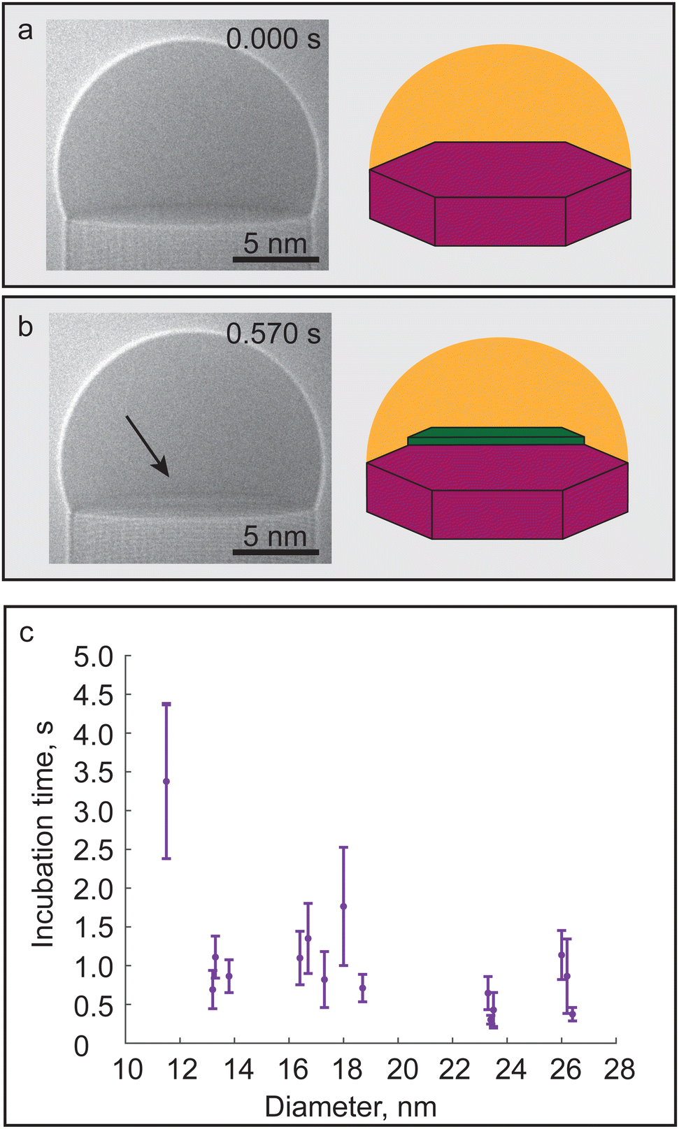 | ||
| Fig. 1 Incubation in GaAs nanowires. (a and b) HRTEM images and schematics showing the incubation process between two step-flow events. Time in the upper right corner of the HRTEM images corresponds to time after a previous GaAs layer was completed i.e. incubation process has started. Incubation process is concluded when a new layer is nucleated indicated by the black arrow in the HRTEM image and the green island in the schematic. In the schematics the liquid Au–Ga–As alloy is shown in yellow, solid GaAs crystal in red and the newly nucleated layer in green. (c) Incubation time as a function of GaAs nanowire diameter shown in purple with error bars representing standard deviations. Each data point corresponds to a nanowire for which 20 events were recorded. | ||
Before discussing the incubation and step-flow process it is worth noting that no change in crystal structure from the original WZ phase was observed as a function of nanowire diameter; therefore it will not be discussed further. To examine the effect of diameter on incubation time, videos of the growth process for nanowires with diameters in the range between 11.5 and 26.5 nm were acquired. The recorded data is shown in Fig. 1c with the purple circles depicting the average calculated incubation time for a nanowire with error bars showing the standard deviations measured across 20 events. The incubation time does not exhibit a size dependency within the 13 to 26.5 nm diameter range. The stability of incubation time suggests that diameter change does not significantly change the net Ga flux to the interface. For the nanowire with 11.5 nm diameter a sharp increase in incubation time was observed. Since this increase was only observed for a single nanowire it is not possible to reach any definite conclusions; however, it could be interpreted as an indication of the dimensions approaching the Gibbs–Thomson radius. As discussed previously in III–V nanowires such as GaAs the GT effect decreases the supersaturation between liquid and solid phase by introducing a correction factor which scales with nanowire diameter. This means that below the critical Gibbs–Thomson radius the overall supersaturation is reduced so much that the nucleation probability of new islands on the LS interface is suppressed, thus stopping the layer-by-layer growth process.28
After a new island is nucleated on the LS interface at the end of the incubation process, the step-flow process begins. Step-flow time here is interpreted as the time between the observation of a newly nucleated island on top of LS interface, as seen in Fig. 2a, until it has covered the whole LS interface again forming a flat LS interface, as depicted in Fig. 2c. The time evolution of one such step-flow event after the initial island nucleation is depicted in Fig. 2a and c using HRTEM images, extracted from videos recorded during growth, and schematics. In order to evaluate the effect of diameter on the step-flow process 21 events were recorded in each of the 15 nanowires investigated covering a span of 11.5 nm to 26.5 nm. In Fig. 2d each of the investigated nanowires is represented by an orange circle where the error bars represent standard deviation observed within the 21 step-flow events recorded.
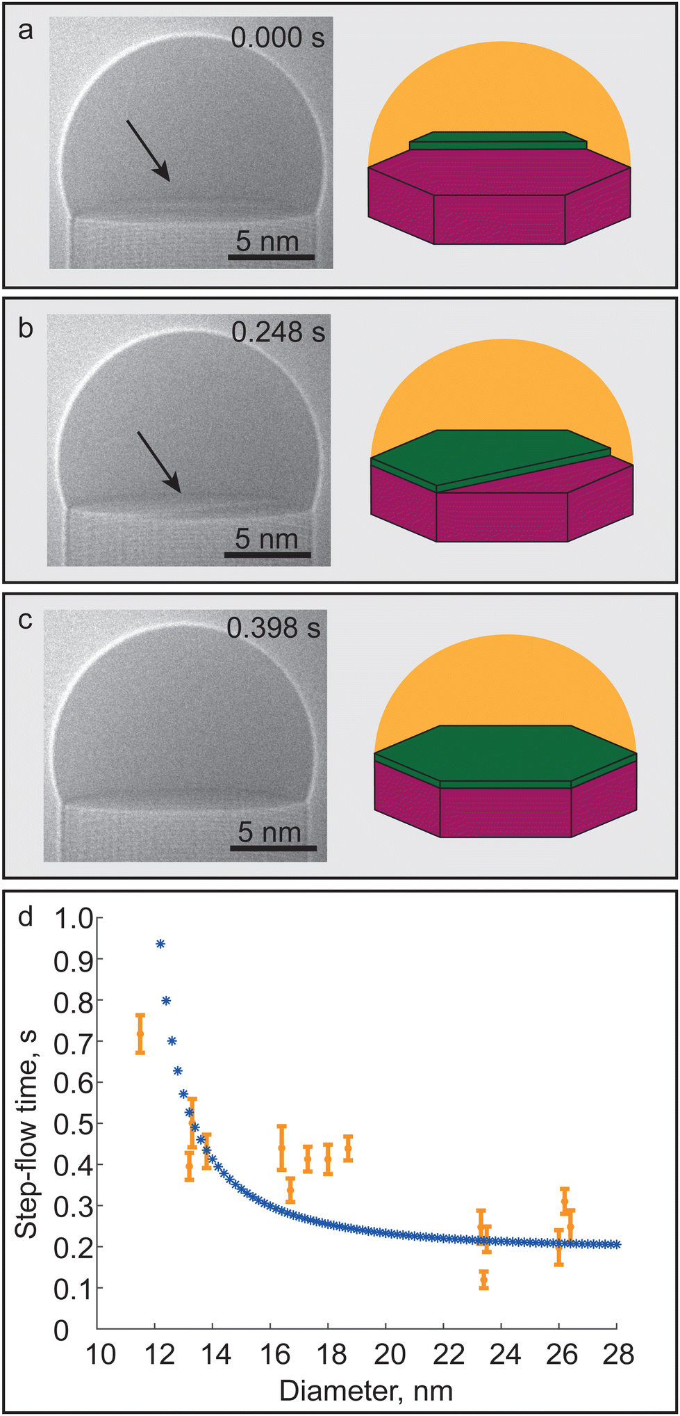 | ||
| Fig. 2 Step-flow in GaAs nanowires. (a–c) HRTEM images and schematics showing the GaAs bilayer step-flow process. Time in the upper right corner of the HRTEM images corresponds to time after a newly formed island was first observed. Black arrow in the HRTEM images points towards the step between covered and uncovered areas of the liquid–solid interface. In the schematics the liquid Au–Ga–As alloy is shown in yellow, solid GaAs crystal in red and the growing bilayer across the liquid–solid interface in green. (d) Step-flow time as a function of GaAs nanowire diameter shown in orange with error bars representing standard deviations. Each data point corresponds to a nanowire for which 21 events were recorded. Blue stars depict the modelled step-flow time curve. | ||
The dynamics of the step-flow remained similar between the different diameter nanowires with the GaAs islands observed at the beginning of the process always being anchored to the TPL for all investigated nanowires. During the step-flow process the layer advanced across the LS interface by incrementally filling large sections of the LS interface switching between convex, concave and straight edged configurations (see Video S1, ESI†). This should not be viewed as a lack of temporal resolution of our system, since this type of step-flow behaviour is consistent with previous in situ studies of nanowire growth.22–24 Images and 2D schematic contours of the faceting of the bilayer for a nanowire not included in the main dataset are shown in SI-3 (ESI†). The video showcases the initial fast growth followed by the slower incremental step-flow advancement across the LS interface. This behaviour has been attributed to the low amount of As atoms in the droplet which is smaller than the amount of As atoms required to cover the whole LS interface.18 In modelling this phenomenon has been termed the stopping effect, where it was shown that the amount of initial LS interface coverage was strongly dependent on the As flow.24,30,31 Contrary to incubation time, our data shows that the step-flow time increases for decreasing nanowire diameter across the examined diameter range, as seen in Fig. 2d.
The step-flow time is known to primarily depend on the AsH3 pressure in the gas phase with the TMGa having an impact only at the extremely low flow range.23 As discussed previously the incremental advancement of step-flow across the LS interface is also shown theoretically to be strongly dependent on the As abundance in the droplet. In the investigated diameter range we observed an increase of step-flow time when approaching smaller diameters which we attribute to a reduced availability of As atoms in the droplet. This observation could be caused by an increased group V material desorption in the droplet due to curvature effects; this is more commonly known as the Kelvin effect.28 In order to explain the observed trend in step-flow time a simplistic model was made; the full details of the model are discussed in SI-1 (ESI†) and in the following, we will discuss only key components of the model.
The model relies on the assumption that step-flow is sensitive only to the changes in the AsH3 supply in the droplet as experimentally demonstrated by Maliakkal et al.,23 This allows us to relate the step-flow time of the As atom flux across the liquid–vapour (LV) interface by using the Hertz–Knudsen equation. The impingement rate (per area) was constant for all nanowires; therefore, an increase in step-flow time is expected to arise because of increase in As vapour pressure surrounding the droplet which in our model is incorporated using the Kelvin equation. The Kelvin effect can be treated as a more specific case of the GT effect with the main difference being that chemical potentials are generally used to describe the state of the system in GT effect, while when using vapour pressures the effect is commonly referred to as the Kelvin effect. The increase in As vapour pressure surrounding the droplet would result in an increased evaporation rate from droplet thus resulting in a reduction of the net impingement rate. According to our model the equation that describes the relationship between step-flow and nanowire diameter is as follows:
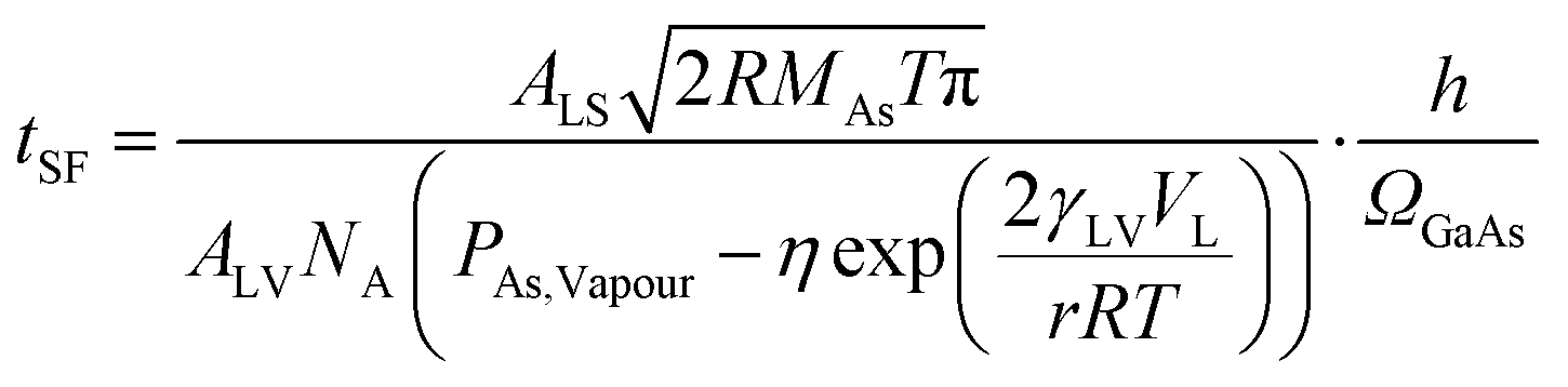
The described model fit is shown in Fig. 2d as the blue curve and can be seen to fit well to the experimental data incorporating both the stable large diameter range and the sharp rise in step-flow time observed for the smallest diameter nanowires. The observed deviations between experimental data and the fitted curve are expected to arise primarily because of the estimated liquid vapour surface energy used in the fitting; more details are provided in SI-1 (ESI†). Therefore, this model demonstrates that the increasing vapour pressure in the droplet can potentially explain the increase in step-flow time. In Fig. 2d we have only chosen to show the model for the diameter range where experimental data was obtained. Further reduction in nanowire diameter, according to our model, would result in the desorption to eventually surpass the material influx to the catalyst droplet resulting in the inability to complete the step-flow process.
The incubation time was not observed to be significantly affected in the investigated diameter range except for the smallest nanowire diameter. The overall robustness and insensitivity observed in incubation time across the majority of investigated diameters indicates that diameter change is not significantly affecting the net Ga flux. A significant increase in incubation time was only observed for one nanowire which could mean that the Ga size effects become significant at smaller diameters than compared to As for the growth conditions used here. It is also possible that a very subtle trend is obscured by the standard deviation of the data which arises due to the probabilistic nature of nucleation.23
The step-flow time was observed to steadily increase across the examined diameter range with a similarly sharp increase in time for the smallest diameter nanowire. This indicates that the change in nanowire diameter primarily affects net impingement of As atoms across the vapour–liquid interface via increasing vapour pressure as shown by our model. The difference in how nanowire diameter acts upon the two processes is likely caused by the inherent differences of elemental As and Ga. In general the concentration of As atoms in the seed particle is assumed to be <1%. This is a direct consequence of the properties of elemental As, such as high vapour pressure and low solubility in Au. In contrast to the volatile As atoms, the Ga atoms readily alloy with Au and typically have a concentration of 20–50% in the droplet.18,21
Based on the model used to fit the step-flow time we speculate that for smaller diameters the net flux across the liquid–vapour (LV) interface is decreased i.e. As atom desorption from the droplet is increased. This would effectively reduce the total amount of As atoms available for growth, therefore, resulting in an increased step-flow time. It has previously been demonstrated by theoretical works that a decrease in As concentration in the droplet can diminish the nucleation of new layers, even completely suppressing it.31–33 This reduction in the driving force for nucleation could be a potential explanation to the presence of the sharp increase in incubation time. Our experimental work has expanded on these theoretical works by showing that the layer-by-layer growth process in GaAs nanowires could be limited by the inability to finish the step-flow process instead of nucleation. Furthermore, an increased desorption of As atoms from the droplet could push the growth into a more As-limited regime, which in extreme cases is predicted to result in particle swelling, since the As supply is not sufficient to reach steady state growth.21,23 However, no swelling of the droplet was observed in our experiments. This was further confirmed by examining the droplet contact angle at the LS interface; we did not find any correlation between contact angle, diameter and the step-flow, incubation process times (see SI-2, ESI†).
Recent investigations into nanowire solid phase stability have also demonstrated the importance of As. In a study by Oliveira et al.,33 using molecular dynamics simulations they showed that As atoms are crucial to prevent dissolution of the solid phase by forming a thin layer on the Au–Ga droplet and being in constant exchange with As atoms at the TPL. They demonstrated that if the number of As atoms in the droplet is insufficient this could lead to the dissolution of the solid phase. In the context of our work this could happen by further reducing the nanowire dimensions under a constant As flux due to increasing desorption rate of As atoms as described by the Kelvin effect. Dissolution of nanowire solid phase or etching has been shown by in situ studies to be connected to amount of Ga atoms in the droplet;34 however, it has not yet been related to the As content in the droplet.
These observations are expected to translate to ex situ nanowire growth. The overall pressure in conventional MOCVD systems is significantly higher (104–105 Pa), however, it is mostly H2. The partial pressures, however, of the precursors are quite similar – the AsH3 partial pressures used here are on the same order as those of conventional MOCVD growths with TMGa flows being slightly lower.25 Increased partial pressures in conventional systems would be expected to increase the rates i.e. decrease the times of the incubation and step-flow processes. Since the main finding in this study involves the As-limited step-flow process, and AsH3 pressures are similar to ex situ partial pressures, we expect this finding to apply also to conventional systems. For molecular beam epitaxy (MBE) nanowire growth rates are generally slower than MOCVD and therefore slightly closer to in situ growth rates; however since the precursors used are different it is difficult to compare the incubation and step-flow processes specifically.
Conclusions
In conclusion, we have investigated how nanowire diameter affects the Ga-limited incubation and As-limited step-flow processes for Au-seeded GaAs nanowires grown in situ. Our results have shown that the incubation time does not change significantly with nanowire diameter except for a sharp increase at the smallest investigated nanowire diameter. This indicates that the Ga net flux remains insensitive to diameter across most of the investigated diameter range. The step-flow time, on the other hand, was observed to gradually increase with decreasing nanowire diameter. This observation indicates that the net impingement of As atoms is reduced, which may be a consequence of the increasing As vapour pressure surrounding the droplet as shown by our model. The observation of the As-limited step-flow time increasing for decreasing diameter is especially important as it provides first experimental evidence suggesting that As net flux is affected by diameter change. This highlights the importance of including both Ga and As flux into further efforts describing the nanowire layer-by-layer growth process.Author contributions
M. M. took part in conceptualization, methodology, validation, formal analysis, investigation, data curation, visualization, project administration, writing – original draft and writing – review & editing. M. T. took part in conceptualization, methodology, investigation and writing – review & editing. E. K. M. took part in methodology, software, validation, formal analysis and writing – review & editing. D. J. took part in validation, investigation, resources, data curation and writing – review & editing. K. A. D. took part in conceptualization, funding acquisition, project administration and writing – review & editing.Conflicts of interest
There are no conflicts to declare.Acknowledgements
The authors acknowledge the Knut & Alice Wallenberg foundation for financial support. The authors would like to thank Sebastian Lehmann for performing the aerosol nanoparticle deposition and Robin Sjökvist for valuable discussions.Notes and references
- E. Barrigón, M. Heurlin, Z. Bi, B. Monemar and L. Samuelson, Chem. Rev., 2019, 119, 9170–9220 CrossRef.
- V. G. Dubrovskii and N. V. Sibirev, J. Cryst. Growth, 2007, 304, 504–513 CrossRef CAS.
- E. K. Mårtensson, S. Lehmann, K. A. Dick and J. Johansson, Cryst. Growth Des., 2020, 20(8), 5373–5379 CrossRef.
- L. E. Fröberg, W. Seifert and J. Johansson, Phys. Rev. B: Condens. Matter Mater. Phys., 2007, 76, 1–4 CrossRef.
- W. Seifert, M. Borgström, K. Deppert, K. A. Dick, J. Johansson, M. W. Larsson, T. Mårtensson, N. Skold, C. P. T. Svensson, B. A. Wacaser, L. R. Wallenberg and L. Samuelson, J. Cryst. Growth, 2004, 272, 211–220 CrossRef CAS.
- V. G. Dubrovskii, N. V. Sibirev, G. E. Cirlin, I. P. Soshnikov, W. H. Chen, R. Larde, E. Cadel, P. Pareige, T. Xu, B. Grandidier, J. P. Nys, D. Stievenard, M. Moewe, L. C. Chuang and C. Chang-Hasnain, Phys. Rev. B: Condens. Matter Mater. Phys., 2009, 79, 1–7 CrossRef.
- C. Soci, X. Bao, D. P. R. Aplin and D. Wang, Nano Lett., 2008, 8(12), 4275–4282 CrossRef CAS.
- E. I. Givargizov, J. Cryst. Growth, 1973, 20, 217–226 CrossRef.
- V. G. Dubrovskii and N. V. Sibirev, Phys. Rev. E: Stat. Phys., Plasmas, Fluids, Relat. Interdiscip. Top., 2004, 70, 7 CrossRef.
- E. Bellet-Amalric, F. Panciera, G. Patriarche, L. Travers, M. Den Hertog, J. C. Harmand, F. Glas and J. Cibert, ACS Nano, 2022, 16, 4397–4407 CrossRef PubMed.
- C. Y. Wen, J. Tersoff, K. Hillerich, M. C. Reuter, J. H. Park, S. Kodambaka, E. A. Stach and F. M. Ross, Phys. Rev. Lett., 2011, 107, 1–4 CrossRef.
- J. B. Hannon, S. Kodambaka, F. M. Ross and R. M. Tromp, Nature, 2006, 440, 69–71 CrossRef PubMed.
- A. D. Gamalski, C. Ducati and S. Hofmann, J. Phys. Chem. C, 2011, 115, 4413–4417 CrossRef.
- F. M. Ross, J. Tersoff and M. C. Reuter, Phys. Rev. Lett., 2005, 95, 1–4 Search PubMed.
- C. Y. Wen, J. Tersoff, M. C. Reuter, E. A. Stach and F. M. Ross, Phys. Rev. Lett., 2010, 105, 1–4 CrossRef.
- S. Kodambaka, J. Tersoff, M. C. Reuter and F. M. Ross, Phys. Rev. Lett., 2006, 96, 1–4 CrossRef PubMed.
- C. B. Maliakkal, D. Jacobsson, M. Tornberg and K. A. Dick, Nanotechnology, 2022, 33(10), 105607 CrossRef CAS.
- C. B. Maliakkal, E. K. Mårtensson, M. U. Tornberg, D. Jacobsson, A. R. Persson, J. Johansson, L. R. Wallenberg and K. A. Dick, ACS Nano, 2020, 14(4), 3868–3875 CrossRef CAS.
- R. Sjökvist, D. Jacobsson, M. Tornberg, R. Wallenberg, E. D. Leshchenko, J. Johansson and K. A. Dick, J. Phys. Chem. Lett., 2021, 12, 7590–7595 CrossRef PubMed.
- M. Tornberg, C. B. Maliakkal, D. Jacobsson, K. A. Dick and J. Johansson, J. Phys. Chem. Lett, 2020, 11(8), 2949–2954 CrossRef CAS.
- D. Jacobsson, F. Panciera, J. Tersoff, M. C. Reuter, S. Lehmann, S. Hofmann, K. A. Dick and F. M. Ross, Nature, 2016, 531, 317–322 CrossRef CAS PubMed.
- J. Harmand, G. Patriarche, F. Glas, F. Panciera, I. Florea, J. Maurice, L. Travers and Y. Ollivier, Phys. Rev. Lett., 2018, 121, 166101 CrossRef CAS PubMed.
- C. B. Maliakkal, E. K. Mårtensson, M. U. Tornberg, D. Jacobsson, A. R. Persson, J. Johansson, L. R. Wallenberg and K. A. Dick, ACS Nano, 2020, 14(4), 3868–3875 CrossRef CAS.
- F. Glas, F. Panciera and J.-C. Harmand, Phys. Status Solidi RRL, 2022, 2100647 CrossRef CAS.
- C. Hetherington, D. Jacobsson, K. A. Dick and L. R. Wallenberg, Semicond. Sci. Technol., 2020, 35 DOI:10.1088/1361-6641/ab6bfd.
- M. Tornberg, C. B. Maliakkal, D. Jacobsson, R. Wallenberg and K. A. Dick, Microsc. Microanal., 2022, 1–9 CrossRef PubMed.
- E. Gil, V. G. Dubrovskii, G. Avit, Y. André, C. Leroux, K. Lekhal, J. Grecenkov, A. Trassoudaine, D. Castelluci, G. Monier, R. M. Ramdani, C. Robert-Goumet, L. Bideux, J. C. Harmand and F. Glas, Nano Lett., 2014, 14, 3938–3944 CrossRef CAS PubMed.
- F. Glas, M. R. Ramdani, G. Patriarche and J. Harmand, Phys. Rev. B: Condens. Matter Mater. Phys., 2013, 195304 CrossRef.
- F. Glas, J. Harmand and G. Patriarche, Phys. Rev. Lett., 2007, 146101 CrossRef PubMed.
- D. P. Wilson, F. Glas, R. R. Lapierre and V. G. Dubrovskii, Proc. Int. Conf. Laser Opt. 2020, ICLO 2020, 2020, vol. 121, p. 197101.
- V. G. Dubrovskii, Cryst. Growth Des., 2017, 17, 2589–2593 CrossRef CAS.
- F. Glas, J. Appl. Phys., 2010, 108, 073506 CrossRef.
- D. S. Oliveira, ACS Appl. Nano Mater., 2021, 4(3), 2903–2909 CrossRef CAS.
- M. Tornberg, D. Jacobsson, A. R. Persson, R. Wallenberg, K. A. Dick and S. Kodambaka, Nano Lett., 2019, 19(6), 3498–3504 CrossRef.
Footnote |
| † Electronic supplementary information (ESI) available. See DOI: https://doi.org/10.1039/d2nh00432a |
| This journal is © The Royal Society of Chemistry 2023 |