DOI:
10.1039/D2NH00384H
(Communication)
Nanoscale Horiz., 2023,
8, 245-255
Temperature-affected nano-deformation behavior of nanometals in ultrahigh-strain-rate formation processes†
Received
15th August 2022
, Accepted 8th December 2022
First published on 9th December 2022
Abstract
As metal forming processes move toward high speed, high throughput, high precision and small scale with temperature dependence, clarifying the fundamental nano-deformation behavior of metals is critical for the optimization of manufacturing processes, and the control of nano-optical, electrical, mechanical or surface properties. Unfortunately, limited by the time scale and sample size, the effect of temperature on the deformation behavior of nano-metals during the ultrahigh-strain-rate forming process remains largely unexplored. This study demonstrates the nonlinear effect of temperature on the formability of nano-metals for the first time. Temperatures below 673 K facilitated the formability of nano-metals benefiting from the temperature-promoted dislocation proliferation process, whereas temperatures above 673 K weakened the plasticity of the nano-metal due to the activation of phase transformation. Frequent phase transition activation and accelerated dislocation annihilation at high temperatures reduced interstitial transport channels and delayed atomic transfer. Based on the temperature response of nano-metals in deformation mechanisms, defect evolution behavior and formability, the constitutive model and nano-deformation mechanism map of nano-metals in ultrahigh-strain-rate forming processes are proposed. The objective of this work is to provide basic support for the reasonable matching of nano-forming technology and processing temperature, and the determination of the optimal process window through fundamental nano-deformation behavior exploration.
New concepts
In this study, we demonstrate a nonlinear effect of temperature on the formability of nano-metals in ultrahigh-strain-rate forming processes for the first time. Unlike the temperature-promoted thermoplastic behavior at low strain rates or quasi-strain rates, high temperatures (<673 K) inhibit the plastic flow behavior of nanometals during ultrahigh-strain-rate shaping processes. The hidden mechanisms of high-temperature-induced phase transformation and high-speed dislocation annihilation processes hindering atomic transport behavior are revealed. A temperature-coupled model based on interstitial diffusion is proposed to describe the anomalous nanomechanical behavior of nanometals under extreme conditions that cannot be described by conventional constitutive models. The main contribution of this study lies in the discovery of the unusual mechanical behavior of nanomaterials at high temperatures and ultrahigh strain rates, and the revealing of the special atomic mechanism behind them, which provides supplements and guidance for material science understanding, shaping precision control and process parameter selection of nano-metals under extreme conditions.
|
Introduction
Metallic nanostructures are gaining augmenting research interest, appreciated by the unusual physical properties, and have been widely used in surface modification,1 surface-enhanced Raman scattering,2 biological/chemical sensing,3 and catalysis4 fields, driving the development of metal nanomaterials towards high speed, high throughput, high precision and small scale with temperature dependence.5,6 It is indispensable to understand the nano-deformation behavior of metals for the optimization of nano-manufacturing process, and the control of nano-optical, electrical, mechanical or surface properties.5
The study of plastic mechanisms at the atomic level is useful for developing new materials with controllable stability and novel manufacturing process matching the material characteristics.7,8 Numerous studies on the nano-deformation behavior of metals at nano-scale such as nanoparticles,9 nanowires,10 nanosheets7 and nanocrystals11 have been carried out at quasi-static or low-strain-rate loadings. The unexpected contribution of the creep mechanism induced by free surfaces,12 lattice diffusion,13 or grain boundary rotation14 to the plasticity of nanomaterials during low-speed deformation processes has been widely reported. For example, Ag nanocrystals with diameters in the range of 15–80 nm exhibited ∼200% uniform elongation under a low strain rate (∼10−3 s−1), benefiting from the surface-diffusion-induced creep mechanism.12,15 With a strain rate of 5 × 10⁻² s−1, the Al9(CoCrFeMnNi)91 high-entropy alloy with multiphase ultrafine grains showed an elongation of 2000% at 1073 K.16 The ultra-high elongation was revealed to be caused by the high grain boundary migration efficiency enhanced by nanocrystals. The fundamental deformation behavior of nano-metals at low strain rates, that is, creep-type deformation, provided a powerful guidance for the understanding and control of the superplastic forming of metallic nanowires using thermomechanical nanomolding.13,17
The laser shock forming, based on a thermal-mechanical conversion process, have been demonstrated to be a high-throughput and flexible technique for nanostructure fabrication.18–20 This non-contact and ultrahigh-strain-rate forming technology provides a promising production route for the direct and controllable formation of nanostructures.5,21 Due to the combined performance of complex factors including ultrahigh strain rates, ultra-short time scale, size effect, and dynamic stress transfer, the high-speed forming process of nano-metals tends to generate different plastic mechanisms, mechanical responses and defect evolution behaviors compared to their bulk counterparts.22,23 Unlike plastic that behaves under a quasi-static state, the ultra-high strain rate deformation process induced by pulsed lasers was divided into dynamic creation and subsequent static evolution of extreme gradient nanocrystals at room temperature.24 The high elastic strain energy stored in the material can sustain the recrystallization process for several weeks. In a typical macroscopic forming process, it is generally accepted that temperature can significantly improve the formability of metals due to the rational combination of hardening behavior and thermoplasticity.25 However, this law may no longer hold for nano-metals owing to the peculiar mechanical behavior caused by size effects and the plastic mechanism activated under extreme conditions. Previous studies have demonstrated the interstitial-mediated superplastic behavior of plasmonic metals during nanoforming processes under ultrahigh strain rates,26 which is significantly different from the conventional mechanical behavior of their bulk counterparts. To the best of our knowledge, the temperature dependence of the nanodeformation behavior of nano-metals during laser shock forming processes is completely unknown, limited by the time scale and sample size, which hinders the understanding of the high-speed forming process of nanostructures.
Although in situ observations of the nanoforming behavior of nano-metals at ultrahigh strain rates are difficult, molecular dynamics (MD) simulation provides a powerful tool for mechanical behavior and plasticity mechanism investigation at short time scales and extreme strain rates.27–30 Herein, we demonstrate the nonlinear effect of temperature on the formability of nano-metals based on MD studies. Temperature-affected nano-deformation behaviors and plastic mechanisms of plasmonic metals in ultrahigh-strain-rate forming processes were studied in this work. The relationship between thermal-induced plastic mechanism transformation, defect evolution, material transfer and formability was revealed. Based on the response of deformation mechanism, defect evolution behavior and formability to the processing temperature, the constitutive relation and nano-deformation mechanism map of metals in ultrahigh-strain-rate forming processes were established. This study explored the thermally affected nano-deformation behavior of nano-metals at ultra-high strain rates, which deviates from the conventional temperature-promoted forming law and provides supplements and guidance for material science understanding, achieving precise control and process parameter selection of nano-metals under extreme conditions.
Result and discussion
Thermal-affected forming behaviors
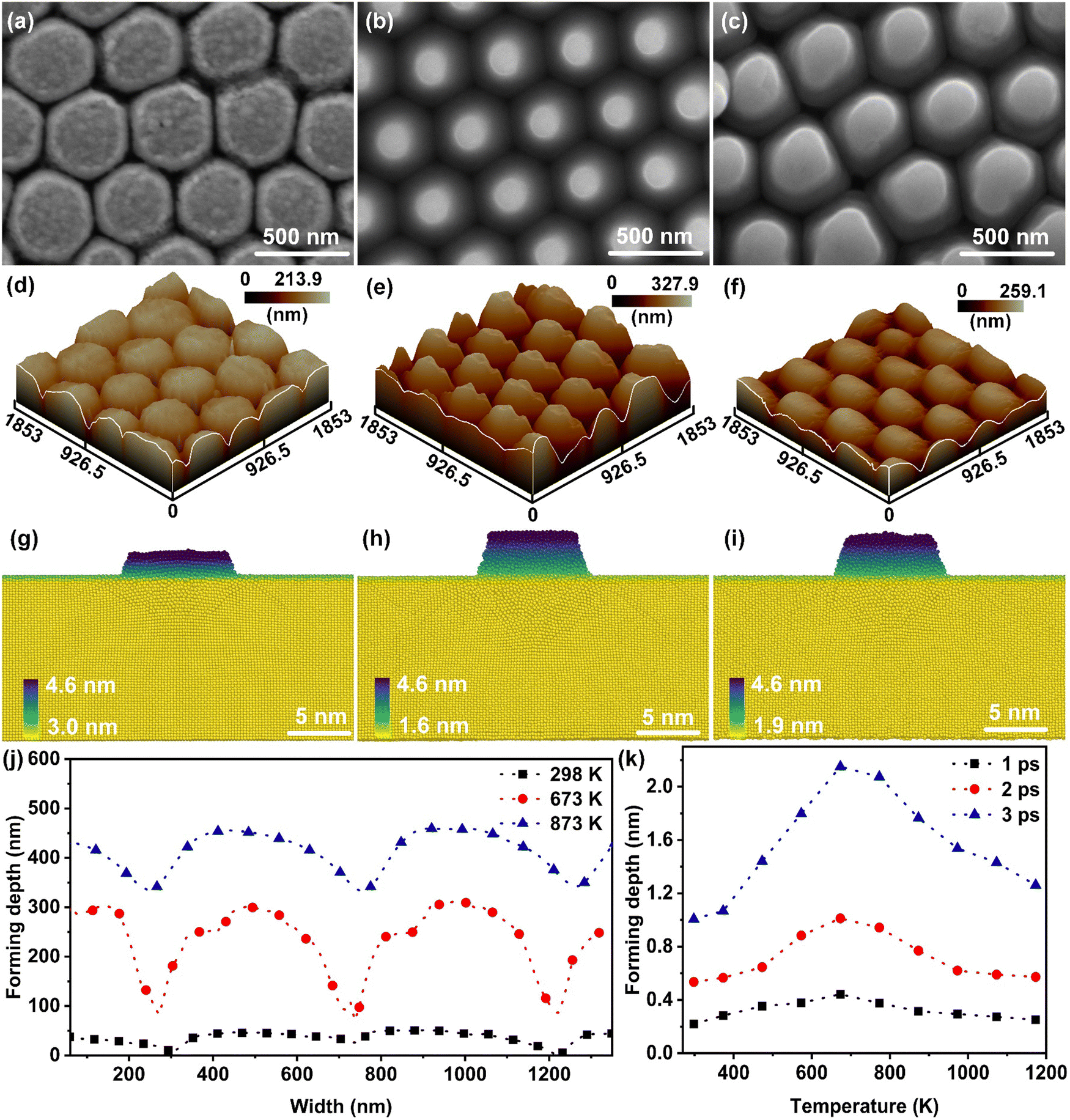
The thermal-affected forming behaviors of nano-metals including Au, Al and Ag were explored via a laser shock imprinting process that provided an ultrahigh-strain-rate (above 106 s−1) plastic deformation scenario.31Fig. 1(a–c) present the SEM images of the Au nanostructures formed at 298 K, 673 K, and 873 K, respectively. Deviating from the empirical law of thermo-promoted forming, the Au nano-sheet exhibited the best forming effect at 673 K. This result was further verified by atomic force microscopic (AFM) tests, as shown in Fig. 1(d–f); the forming depths of the nanostructures were determined to be about 36.1 nm, 219.4 nm, and 118.2 nm, respectively. While the maximum aspect ratio of the Au nanostructure was obtained at 673 K, the Au nanostructures showed a smoother surface and a sharper edge (Fig. 1(j)). Moreover, similar phenomena were observed in Al and Ag nano-sheets (Fig. S1, ESI†).
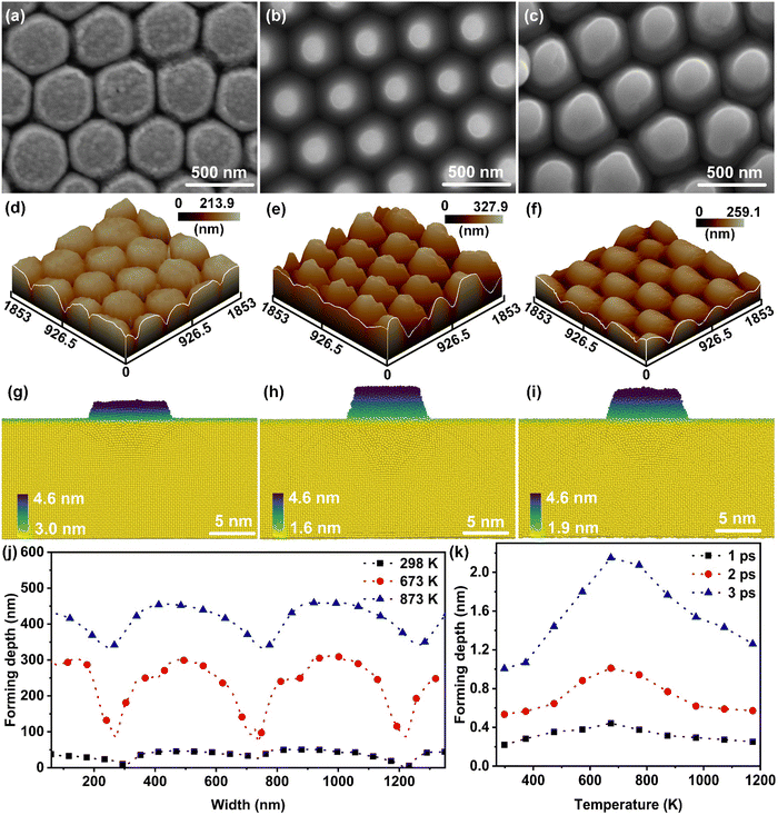 |
| | Fig. 1 Thermal-affected laser shock forming behaviors of Au films. (a–c) SEM images of the Au nanostructures formed at 298 K, 673 K, and 873 K, respectively. (d–f) Three-dimensional morphologies of the Au nanostructures corresponding to figures a–c. (g–i) Snapshots of the Au nanostructures (4 ps) at 298 K, 673 K, and 873 K, respectively. (j) Two-dimensional profiles of the Au nanostructures corresponding to figures a–c. (k) Forming depth versus processing temperature curves. | |
The effect of temperature on the forming behavior of nanometals was verified by MD simulations; the consistency between the experimental and simulated results can be demonstrated by the snapshots of the Au nanostructures (Fig. 1(g–i)) simulated at 298 K, 673 K, and 873 K, respectively, where the atoms were colored according to the coordinates of the atoms in the z-axis direction. The MD results indicated that the forming depth of the Au nanostructures at 298 K, 673 K, and 873 K was 1.6 nm, 3 nm and 2.7 nm, respectively, which was consistent with the evolution trend of the forming depth in the experiments (Fig. 1(a–c)). From the curves of forming depth versus processing temperature (Fig. 1(k)), it can be found that the temperature exhibited a nonlinear effect on the formability of nano-metals under ultrahigh strain rates; similar phenomena were also observed in the simulation results of Ag and Al nano-sheets (Fig. S2(a) and (b), ESI†). Additionally, the correlation between the dynamic deformation behavior of nano-metals at ultra-high strain rates and shock wave transmission is discussed in the ESI† (Supplementary notes and Fig. S3). Based on the above-mentioned experimental and simulation results, we considered that there was a critical temperature range (around 673 K) for the thermal-promoted formability of nano-metals. For the sake of description, we defined the case where the processing temperature is lower than the critical temperature as the thermal-promoted formability stage, and the case above the critical temperature as the thermal-weakened formability stage.
Deformation mechanism in thermal-promoted formability stage
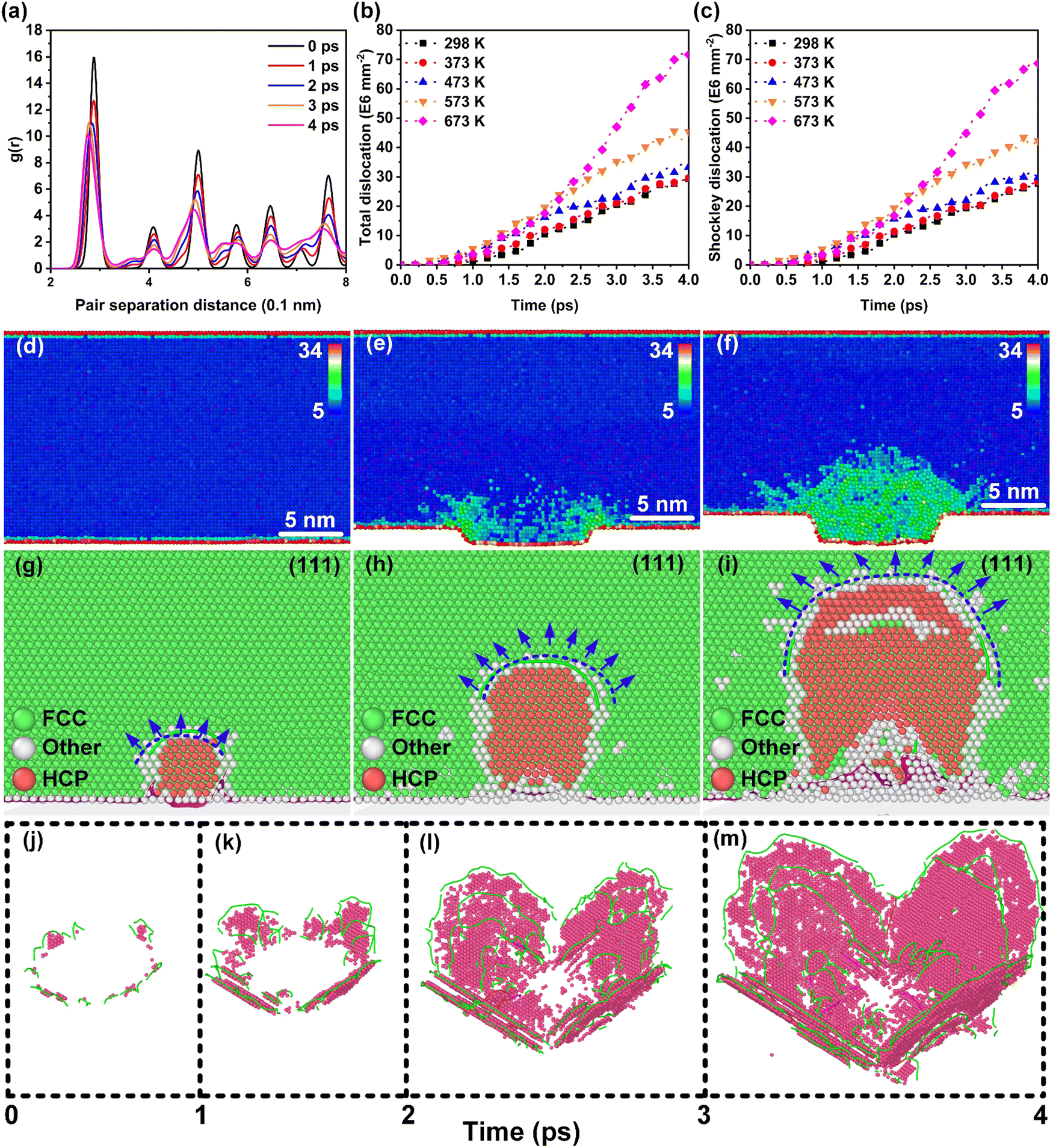
Considering the correlation between the plastic behavior and lattice defects of nano-metals, the evolution behavior of defects was emphatically explored. The radial distribution function (RDF) was used to analyze the lattice structure transformation during the dynamic deformation process, as shown in Fig. 2(a). The RDF curve at 0 ps showed an initial FCC lattice. Further, the RDF curves indicated that Au retained the characteristics of the FCC lattice as the deformation proceeds (1–4 ps), implying the stability of the lattice during deformation at ultra-high strain rates in the thermal-promoted formability stage. The centro-symmetry parameter (CSP) results displayed in Fig. 2(d–f) demonstrate that the low strain area located at the root of the Au nanostructure was the core area where the lattice defects existed, except for the severe plastic deformation area inside the nanostructures.
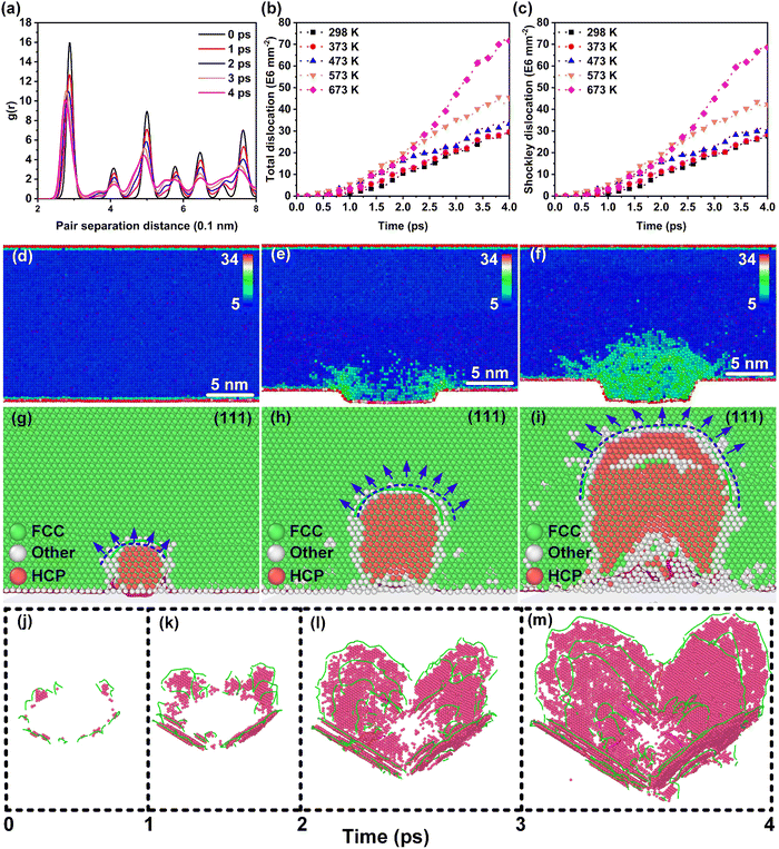 |
| | Fig. 2 Radial distribution function curves and defect evolution behavior. (a) Radial distribution function evolution of the Au nanostructures at different time-steps (573 K). (b) Evolution of the total dislocation density in the thermal-promoted formability stage. (c) Evolution of the Shockley dislocation density in the thermal-promoted formability stage. (d–f) Evolution of CPS at 0 ps, 1 ps and 2 ps, respectively. (g–i) Shockley dislocation proliferation process. (j–m) Dynamic multiplication process of the lattice defects in the ultrahigh-strain-rate forming process at 0.8 ps, 1.8 ps, 2.7 ps, and 3.4 ps, respectively. | |
The dynamic dislocation density evolution curves in the thermal-promoted formability stage are shown in Fig. 2(b). At this stage, the introduction of a temperature field greatly augmented the dislocation density by enhancing the dislocation germination and proliferation processes. Unlike the dislocation mechanism of bulk materials, the size effect results in higher flow stress during the plastic deformation of nanomaterials, which promotes the advanced activation of partial dislocations. Temperature-accelerated Shockley dislocation (1/6 〈112〉) proliferation processes were the primary reason for the rise in the dislocation density of nano-metals, as shown in Fig. 2(c). Hence the dominant mechanism for the plastic deformation of nano-metals was partial dislocation nucleation during the thermal-promoted formability stage. Additionally, the proliferation process of Shockley dislocations along {111} is presented in Fig. 2(g–i). The proliferation mechanism of Shockley dislocations in nano-metals during the ultrahigh-strain-rate forming process conformed to the Frank-Read law,32 with the loading of laser-induced shock waves. The dislocation evolution behaviors of Ag and Al were consistent with those of Au proven by the dislocation density curves in Fig. S4 (ESI†).
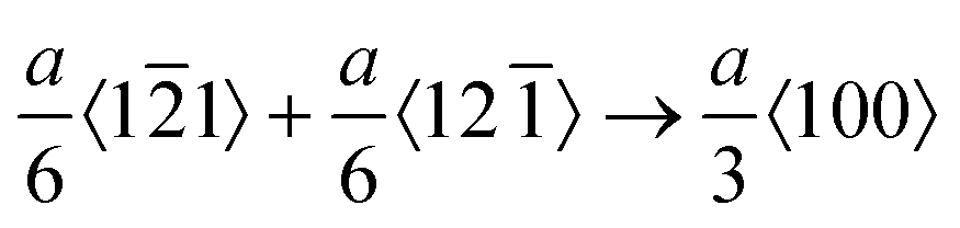
We additionally consider the feasibility of the hardening behavior caused by the dislocation reaction, when the dislocation density substantially increases. The snapshots of the dynamic defect multiplication process of Au at 573 K are present in Fig. 2(j–m). The primary defects that dominate plastic deformation, including dislocations and intrinsic stacking faults, were symmetrically distributed within the Au nanostructure. As the shock wave propagates, the evolution mechanism for lattice defects in the metal target is proven to be the proliferation of Shockley dislocations and the continuous growth of intrinsic stacking faults. The dislocation reactions including the Lomer–Cottrell and Hirth locks that may cause strain hardening behavior are shown in Fig. S5 (ESI†). In the case of the Lomer–Cottrell lock (Fig. S5(a), ESI†), the dislocation interaction can be expressed as follows:
| | 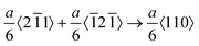 | (1) |
where
a is the lattice parameter. The Hirth lock, whose slip direction deviated from the close-packed direction [110] of the FCC lattice, was also observed in Fig. S5(b) (ESI
†); and the Hirth interaction can be expressed as follows:
| |  | (2) |
Although the above-mentioned dislocation interactions and reactions are common factors in the hardening of FCC-type pure metals,33 Au exhibited a very-sparse dislocation lock-density (<1.1%) during the ultrahigh-strain-rate forming process, as shown in Fig. S6 (ESI†). The dislocation reaction frequency shows low sensitivity to the increase in dislocation density caused by rising forming temperatures. Unlike the strain hardening beyond the yield stress at low strain rates, the hardening behavior of nanomaterials is weakened at ultra-high strain rates.
Deformation mechanism in thermal-weakened formability stage
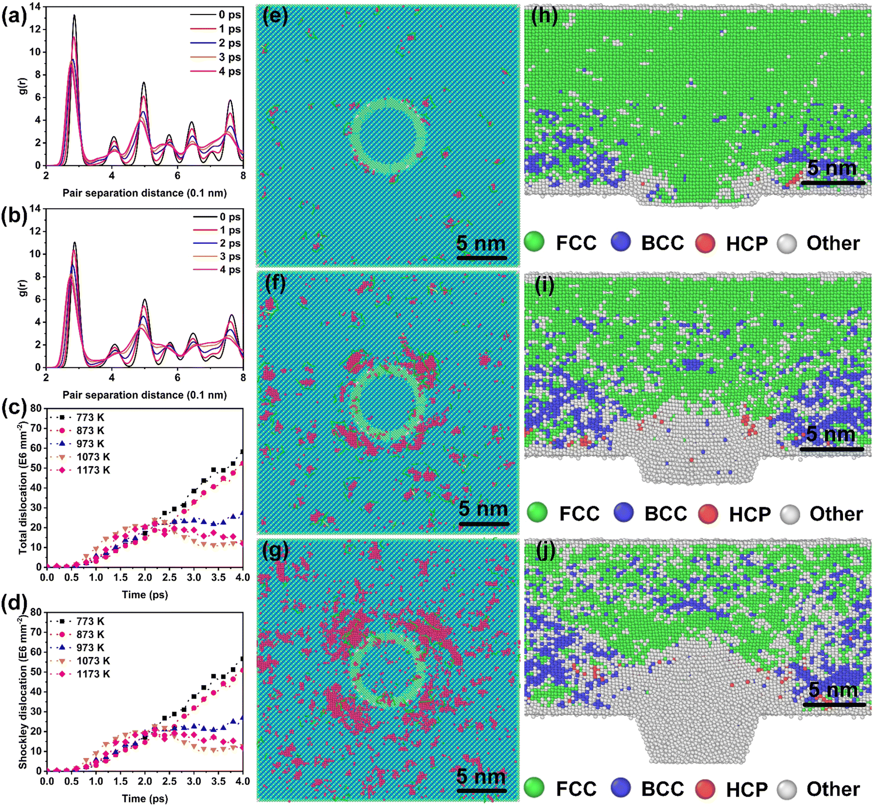
Fig. 3(a) and (b) provide the dynamic RDF curves of Au at 773 K and 973 K, respectively. At 773 K, the evolution behavior of the nearest neighbor peak was similar to the thermal-promoted formability stage. By contrast, the peak intensity was significantly reduced at 973 K, while the nearest neighbor peak was lost at 4 ps (Fig. 3(b)). This indicated that the FCC lattice was severely destabilized during the ultrahigh-strain-rate forming process of the thermal-weakened formability stage. Dynamic dislocation evolution characteristics were extracted in the thermal-weakened formability stage, as shown in Fig. 3(c) and (d). It can be found that the high temperature had a negative effect on the multiplication of dislocations, and the dislocation density exhibited a decreasing trend in this stage. In particular, there was an obvious dislocation annihilation behavior when the temperature exceeded 973 K. The dislocation evolution behavior of Ag nanostructures (Fig. S7, ESI†) also verified the universality of the dislocation annihilation behavior at high temperatures.
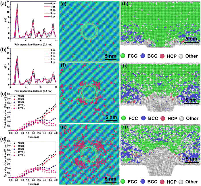 |
| | Fig. 3 Defect evolution in the thermal-weakening formability stage: (a) radial distribution function curves of the Au nanostructure at 773 K. (b) Radial distribution function evolution curves of the Au nanostructure at 973 K. (c) Evolution of the total dislocation density. (d) Evolution of the Shockley dislocation density. (e–g) Snapshots of DXA results (1073 K) at 1 ps, 2 ps and 3 ps, respectively. (h–j) Snapshots of common neighbor analysis results (1073 K) at 1 ps, 2 ps and 3 ps, respectively. | |
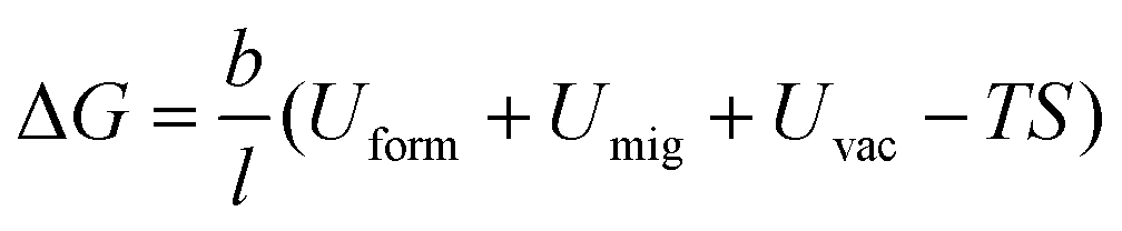
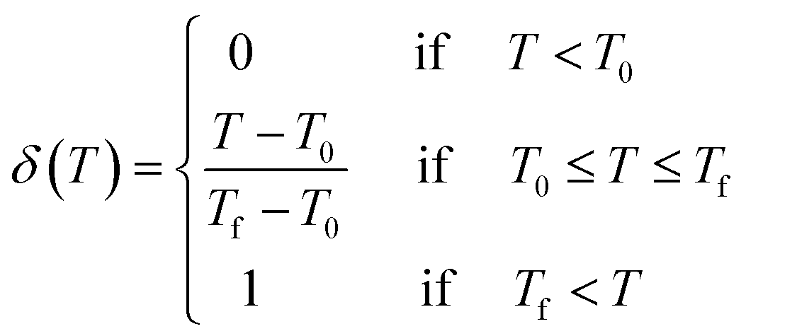
Different from the cross-slip annihilation governing mechanism driven by thermal-activated slip in the thermal-promoted formability stage, the frequent interaction of dislocations with vacancies is considered to be the key factor in dislocation annihilation and reduction of dislocation density when the critical temperature is exceeded. The disparity in dislocation density caused by the annihilation mechanism can be expressed by the energy barrier for dislocation annihilation (ΔG) in eqn (3):34
| | 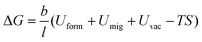 | (3) |
where
b represents the magnitude of the Burgers vector and
l the average length of dislocation annihilation.
G consists of four parts: dislocation formation energy term (
Uform), migration energy term (
Umig), energy contribution of vacancies (
Uvac), and statistical entropy contribution (
TS), respectively. In particular,
Uvac is related to the chemical work (
Wv) induced on the dislocation segment, and a piecewise function (
δ(
T)) is introduced to incorporate and distinguish the changes in the dislocation annihilation mechanism at different temperature stages, which can be expressed as follows:
35| | 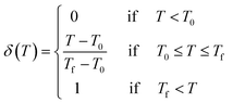 | (5) |
In this study, T is the processing temperature, T0 the critical temperature, and Tf a constant of 873 K. By combining eqn (4) and (5), it can be found that further increases in temperature significantly reduce the dislocation annihilation energy during in the thermal-weakened formability stage. Furthermore, defect visualization results (Fig. 3(e–g)) indicated that the dislocations and stacking faults were distributed in fragments that were significantly different from the concentrated and continuous distribution characteristics of defects in the thermal-promoted formability stage. The thermal-induced FCC to BCC phase transformation can be observed from the snapshots of common neighbor analysis presented in Fig. 3(h–j). The BCC lattice appeared in the high-stress area along with the transmission of the stress waves.
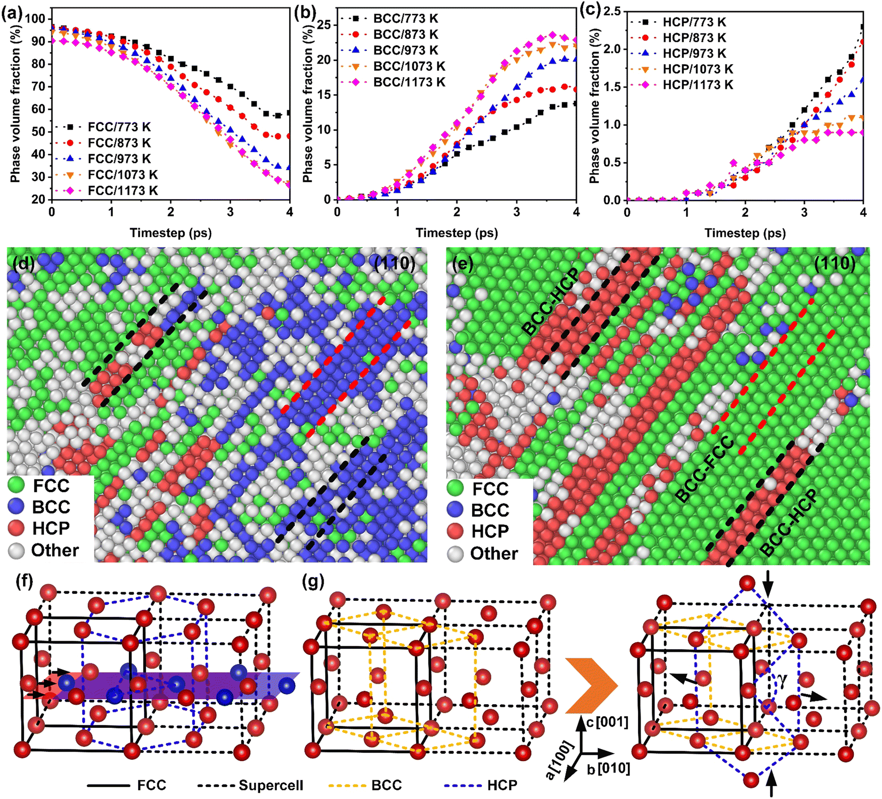
The phase transformation behavior at high temperatures and ultrahigh strain rates was comprehensively studied, as shown in Fig. 4 and Fig. S8 (ESI†). Except for the FCC–HCP lattice transformation guided by the Shockley dislocations (Fig. 4(f)), a high-volume fraction transformation of FCC–BCC phase occurred. Accompanying the decrease (>50%) in the volume fraction of the FCC lattice (Fig. 4(a)), the metastable BCC phase (Fig. 4(b)) was significantly increased (>20%). When the stress wave rebounds were activated (>3.8 ps), the metastable BCC phase transformed into FCC and HCP phases, evidenced by the recovery of the FCC phase and a continuous increase in the HCP phase (Fig. 4(d) and (e)). Hence, the phase transformation behaviors during the thermal-weakened formability stage were summarized into three categories: FCC–HCP, FCC–BCC–HCP and FCC–BCC–FCC, respectively. The phase transformation pathway can be described by the Bain model,36–38 as shown in Fig. 4(g). The direction of the compressive stress was along the [00![[1 with combining macron]](https://www.rsc.org/images/entities/char_0031_0304.gif) ] crystal direction; lattice distortion was manifested as the stretching of the basis vectors a and b, and the compression of c, which transformed the FCC lattice into a metastable BCC structure. The orientation relations between the origin FCC and metastable BCC lattices were [100]FCC//[110]BCC and (111)FCC//(110)BCC. Subsequently, the deformation of the crystallographic plane (110)BCC changed the angle γ (Fig. 4(g)) from 70.53° to 60° between two (110)BCC diagonals, causing the phase transformation from BCC to HCP. Combining the dislocation evolution and phase transformation results, it can be concluded that the dislocation-mediated plastic deformation mechanism was ineffective, when the temperature exceeds 973 K. This was attributed to the thermal-induced phase transformation and the accelerated annihilation of dislocations. In contrast, the primary plastic mechanism was replaced by phase transformation in the thermal-weakened formability stage.
] crystal direction; lattice distortion was manifested as the stretching of the basis vectors a and b, and the compression of c, which transformed the FCC lattice into a metastable BCC structure. The orientation relations between the origin FCC and metastable BCC lattices were [100]FCC//[110]BCC and (111)FCC//(110)BCC. Subsequently, the deformation of the crystallographic plane (110)BCC changed the angle γ (Fig. 4(g)) from 70.53° to 60° between two (110)BCC diagonals, causing the phase transformation from BCC to HCP. Combining the dislocation evolution and phase transformation results, it can be concluded that the dislocation-mediated plastic deformation mechanism was ineffective, when the temperature exceeds 973 K. This was attributed to the thermal-induced phase transformation and the accelerated annihilation of dislocations. In contrast, the primary plastic mechanism was replaced by phase transformation in the thermal-weakened formability stage.
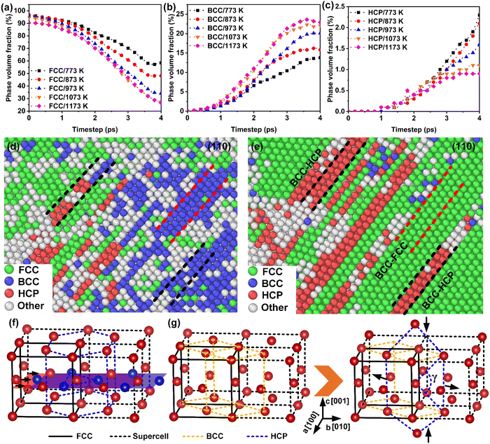 |
| | Fig. 4 Dynamic phase transformation process of Au in the thermal-weakened formability stage. (a) Phase volume fraction of the FCC lattice. (b) Phase volume fraction of the BCC lattice. (c) Phase volume fraction of the HCP lattice. (d) and (e) Snapshots of the common neighbor analysis results at 4 ps and 7.8 ps, respectively. (f) Schematic diagram of the FCC–HCP phase transformation. (g) Schematic diagram of the FCC–BCC–HCP phase transformation. | |
Deformation mechanism-affected material transfer process
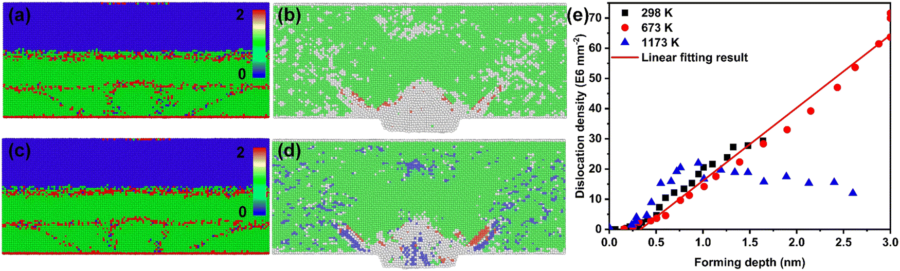
The previous sections discussed the effect of temperature on the formability and the plasticity mechanism of nano-metals in ultrahigh-strain-rate forming processes. This section focuses on the analysis of the relationship between temperature-induced changes in the plasticity mechanism and formability. The forming process can be simply described as a material transfer process, that is, the transfer of material from the target material to the mold. At ultra-high strain rates, the orderly movement of interstitials along with the propagation of the shock waves can be observed in the Wigner-Seitz defect analysis results shown in Fig. 5(a) and (c), which is consistent with our previous research results.26 In Fig. 5(a) and (c), the occupancy of 0 indicates a vacancy, the occupancy of 1 represents a normal position atom, and the occupancy of 2 is an interstitial. Unlike the macroscopic forming process that is directly guided by the plasticity mechanism of the target, the material transfer process of nano-metals is mediated by interstitials in the ultrahigh-strain-rate forming process. In addition, the distribution of interstitials coincided with the stacking faults and partial dislocations, implying that these are the transport channels of the interstitials (Fig. 5(b) and (d)). The dislocation is a favorable channel for interstitial transport, corresponding to the deformation-assisted diffusion mechanism.39
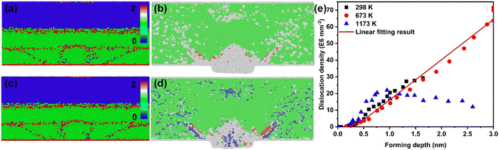 |
| | Fig. 5 Material transfer mechanism in the laser shock forming process. (a) Snapshot of the atomic distribution colored by occupancy at 298 K. (b) Snapshot of the common neighbor analysis result at 298 K. (c) Snapshot of the atomic distribution colored by occupancy at 1173 K. (d) Snapshot of the common neighbor analysis result at 1173 K. (e) Dislocation density versus forming depth curves at different temperatures. | |
In the thermal-promoted formability stage, the plastic behavior of nano-metals is mediated by dislocations, and the increase in temperature accelerates the nucleation and proliferation processes, which provide sufficient channels for the movement of the interstitials and facilitate the improvement of formability. There is an approximate linear relationship between the forming depth and the dislocation density (Fig. 5(e)). However, this linear relationship is deviated at the thermal-weakened formability stage, which means that the hidden mechanism for the weakened formability is the annihilation of dislocations at high temperatures. The reduced atomic transport channels result in a slower material transfer process and weakened formability.
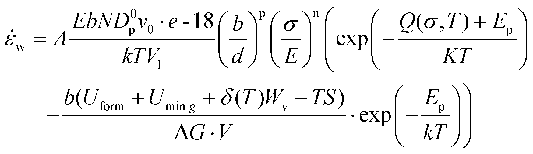
Constitutive model and deformation mechanism map
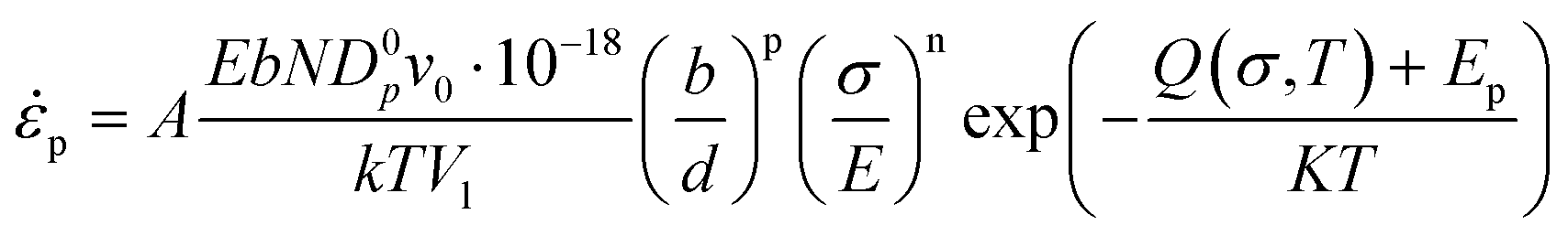
The mechanical behavior of nano-metals at ultrahigh strain rates is difficult to describe using ordinary constitutive models due to the activation of special plasticity mechanisms, abnormal softening behavior, and nonlinear influence of temperature under size-effects and extreme deformation conditions. The deformation of polycrystalline metals with diffusion-type plastic mechanism is usually described by the following constitutive relationship:40| |  | (6) |
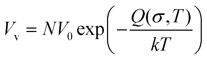
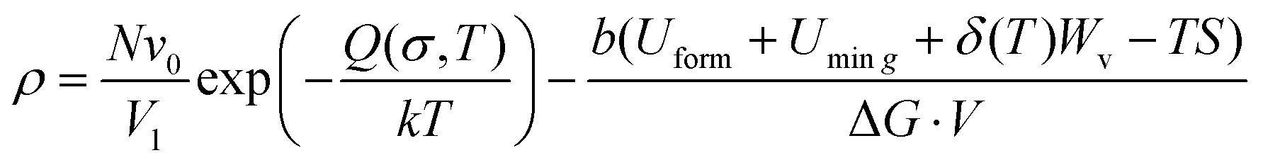
where E is Young's modulus, σ the applied stress, b the Burgers vector, d the grain size, T the processing temperature, and k the Boltzmann constant. The above-mentioned parameters for superior plasmonic nano-metals mentioned in this study are listed in Table S1 (ESI†). In addition, D is the diffusion coefficient of atoms, and can be calculated as follows:41where g is the atomic diffusion component related to the dislocation density (g ≈ ρ·10−18)41 and Dp and Dl the dislocation pipe diffusion coefficient and lattice diffusion coefficient, respectively. According to the analysis results of temperature-affected dislocation density and formability in this work, the movement of interstitials followed the law of dislocation pipe diffusion. Therefore, the lattice diffusion component was ignored, and the diffusion coefficient (D ≈ Dinter) of the interstitials at ultrahigh strain rates is expressed as follows:41where ρ represents the dislocation density. Eqn (8) indicates that the diffusion behavior of interstitials is positively correlated with the dislocation density, which is consistent with our research results. In addition, the dislocation density of metals is significantly reduced when the processing temperature exceeds the critical temperature, due to the activation of the phase transition mechanism and the occurrence of the accelerated dislocation annihilation behavior. We approximate the actual dislocation density ρ above the critical temperature (thermal-weakened formability stage) as follows:where ρp and ρa are the dislocation proliferation density and dislocation annihilation density, respectively. At the thermal-promoted formability stage, the dislocation annihilation behavior was ignored (ρ ≈ ρp) since the dislocation density maintains an approximately linear growth trend. The ρp is given by Vv/Vl, where Vv is the nucleation rate of dislocations per unit volume, and Vl is the nucleation rate within the unit dislocation line. According to the transition state theory, Vv can be calculated as follows:42| |  | (10) |
Combining eqn (4), (5), (9) and (10), the actual dislocation density ρ above the critical temperature can be expressed as follows:| |  | (11) |
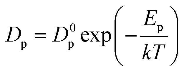
where V is the volume of sample. However, the correlation between Dp and the processing temperature can be further established by the Arrhenius law as follows:43| |  | (12) |
where Ep is the activation energy of dislocation pipe diffusion and D0p the pre-exponential. Hence, combining eqn (6), (8), (11) and (12), it can be concluded that the constitutive relationship of interstitials-mediated nano-deformation in the thermal-promoted formability stage can be expressed as follows:| |  | (13) |
while the constitutive relationship of interstitials-mediated nano-deformation in the thermal-weakened formability stage can be expressed as follows:| |  | (14) |
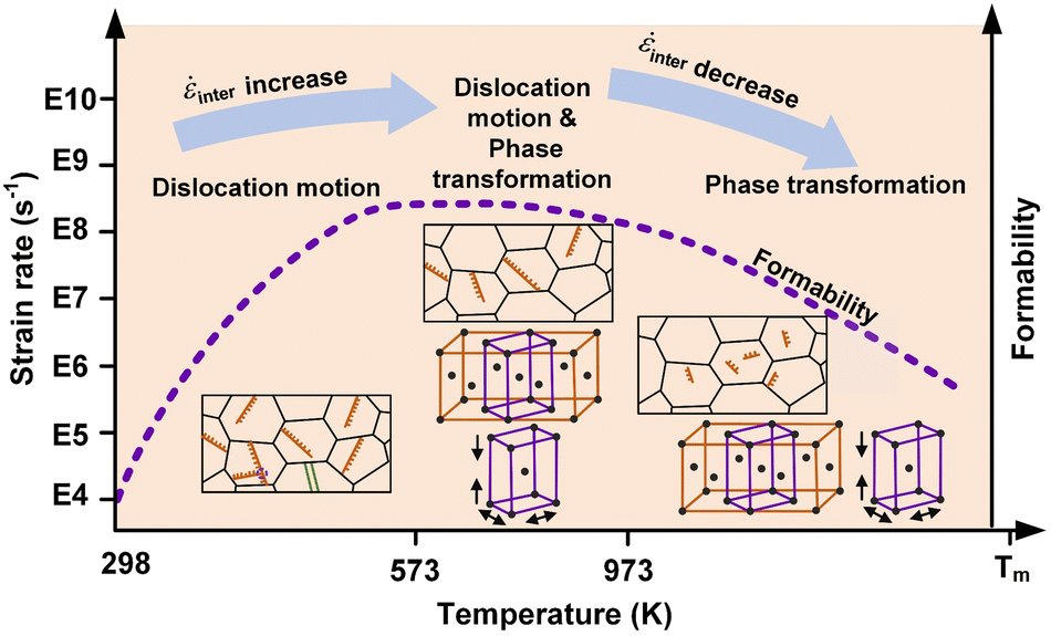
Relying on the special forming behavior of nano-metals under ultrahigh strain rates, the macro-forming mechanism map under quasi-static or low strain rates cannot accurately describe the material responses in the laser shock forming process.44,45 We re-summarized the deformation mechanism map of nano-metals in the ultrahigh-strain-rate forming process, as shown in Fig. 6. Since the strain rate variation is primarily effected by the diffusion behavior of interstitials controlled by the plastic mechanism transformation and defects evolution behaviors at elevated temperatures, the aforementioned ![[small epsi, Greek, dot above]](https://www.rsc.org/images/entities/i_char_e0a1.gif) p and w will be denoted by inter hereafter, which qualitatively expresses the influence of the plastic mechanism transformation on the formability of nano-metals in ultrahigh-strain-rate forming processes. Unlike the traditional forming process, the transformation of the plasticity mechanism of nano-metals at ultrahigh strain rates is directly related to the Kelvin temperature.
p and w will be denoted by inter hereafter, which qualitatively expresses the influence of the plastic mechanism transformation on the formability of nano-metals in ultrahigh-strain-rate forming processes. Unlike the traditional forming process, the transformation of the plasticity mechanism of nano-metals at ultrahigh strain rates is directly related to the Kelvin temperature.
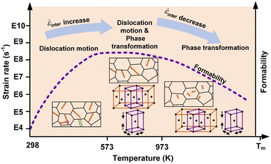 |
| | Fig. 6 Nano-deformation mechanisms of nano-metals classified by temperatures. | |
When the processing temperature is below 573 K, the strain of nano-metals was accommodated by the partial dislocation, and the rise in temperature accelerated the proliferation process, which was conducive to the movement of interstitials and led to an increase in inter. There was a transition stage of the deformation mechanism between 573 K and 973 K, where the dislocation annihilation process caused by the interaction of dislocations and vacancies was greatly accelerated, and the thermal-induced phase transformation was gradually established as the dominant deformation mechanism. At high temperatures (above 973 K), the strain of nano-metals was mediated by a reversible phase transition mechanism, and the dislocation density was significantly reduced accompanied by the fragmentized distribution characteristics. The reduction of the atomic transport channel slowed down the transfer process of the interstitials, resulting in a decrease in inter.
Conclusion
In this work, we studied the temperature-affected nano-deformation behaviors of nano-metals in ultrahigh-strain-rate forming processes. The plasticity mechanisms at different temperatures were determined, and the correlation between defect evolution behavior and material transfer was comprehensively revealed. The constitutive relations and nano-deformation mechanism map of nano-metals in the ultrahigh-strain-rate forming process were proposed. Some important conclusions are listed below:
(1) Deviating from the conventional temperature-promoted forming law, the processing temperature has a nonlinear effect on the formability of nano-metals at ultra-high strain rates.
(2) The deformation mechanism of nano-metals in the thermal-promoted formability stage was partial dislocation motion, and the strain in the thermal-weakened formability stage was mediated by reversible phase transformation.
(3) Temperature promoted the proliferation of dislocations in the thermal-promoted formability stage; a further rise in temperature resulted in a high-speed dislocation annihilation process in the thermal-weakened formability stage, caused by the interaction of dislocations and vacancies.
(4) The hidden reason for the weakening of the formability at high temperatures was that the transformation of the plastic mechanism and the accelerated dislocation annihilation process delayed the movement of interstitials.
Simulation and experimental methods
MD simulations
To reveal the universality of the dynamic plastic deformation behavior of nano-metals in laser shock forming processes, we performed MD simulations on superior plasmonic materials including Al, Au and Ag. MD simulations were executed using the large-scale atomic/molecular massively parallel simulator (LAMMPS).46 As shown in Fig. S9(a) (ESI†), the MD model consisted of a target layer and a mold layer (Si). The lengths of the target layer in x, y, and z directions were set to 70a, 70a, and 30a (a is the lattice parameter of the target material), respectively. The global length (Fig. S9(b), ESI†) of the mold layer in x, y, and z directions was 28.6 nm, 28.6 nm, and 4 nm, respectively. The mold layer was structured by deleting atoms in a cone; the central axis of the cone was z; the radius at lo and hi was 3 nm and 4 nm; and the bounds for diameter were from 1 nm to 4 nm. The interval between the mold layer and the target layer along the z-axis direction was set at 4 nm.
The interaction between pure metal atoms was described by the embedded atom model (EAM) potential,47 and the Tersoff potential was selected to describe the interaction of Si atoms in the mold.48 The interactions between the metal atoms and Si atoms were represented by the Lennard-Jones (L-J) potential with a global cutoff of 4.397 Å. The detailed L-J parameters between the metal atoms and Si atoms are listed in Table S2 (ESI†). The model was first optimized using the conjugate gradient (CG) algorithm, and then the Nose–Hoover thermostat and Nose/Hoover pressure barostat were used for heating and relaxation in a NPT ensemble. The heating rate was set to 10 K ps−1, and the heated model was kept at a target temperature for relaxation. During the relaxation process, the pressures in x, y, and z directions were set to zero with a duration of 60 ps. In this work, the mold layer was simplified to a rigid body, and the laser shock forming processes were simulated in temperatures ranging from room temperature (298 K) to near melting point. Before the forming process was performed, an initial velocity of 1 Km s−1 was given to the target layer. The laser shock forming process was assumed to be carried out at constant temperature to investigate the impact of temperature on the forming process. The shock process was thus performed in the NVT ensemble with a Nose–Hoover thermostat, and the excellent temperature control effects can be observed in Fig. S9(c) (ESI†). The atom visualization, phase transition and defect analysis were executed using an open visualization tool (OVITO), common neighbor analysis and dislocation extraction algorithm (DXA), respectively.49
Laser shock forming experiments
The laser shock forming of the metallic nano-arrays was implemented to verify the correctness of the simulation results. A thermostatic platform with a temperature setting of 298 K, 673 K, and 873 K was used as the heat supply equipment. The laser shock forming experiments were performed using a nanosecond laser, and the laser pulse with a frequency of 1 Hz was offered by a pulsed solid-state laser (Nimma-900). Laser parameters are as follows: the laser energy was 600 mJ; the pulse duration was 7 ns; the wavelength was 1064 nm, and the focused spot radius was 2.5 mm. The target materials were prepared by magnetron sputtering (DM200), and the target materials were composed of a substrate, a connecting layer and a deposited layer (Fig. S9(d), ESI†). An Al foil with a thickness of 3 μm was selected as the substrate, and a pure Ti film with a thickness of 10 nm was sputtered on the surface of the substrate as the connecting layer. The deposited layer with a thickness of 100 nm, including pure Al, Ag and Au, was eventually sputtered on the surface of the connecting layer. The porous anodized aluminium oxide (AAO) molds were used for nanoforming (Fig. S9(e) and (f), ESI†). The geometrical parameters of the mold are as follows: the center spacing of the holes was ∼450 nm, the diameter of the holes was ∼200 nm, and the thickness of the mold was ∼220 nm. Graphite was selected as the absorber layer to induce high-quality plasma, and the Al foil with a thickness of 4 μm was used as the sacrificial layer to prevent the ablation of the target layer. The morphology and forming depth of the nanostructures were analyzed by scanning electron microscopy (SEM, TESCAN, MIRA3) and atomic force microscopy (AFM, MicroNano, D-5A), respectively.
Conflicts of interest
There are no conflicts to declare.
Acknowledgements
This work was supported by the National Natural Science Foundation of China (Grant No. 51901162). The authors thank the support of the National Talent Program of China.
References
- Y. Yoon, D. Kim and J. B. Lee, Micro Nano Syst. Lett., 2014, 2, 1–18 CrossRef.
- Y. Yang, C. Gu and J. Li, Small, 2019, 15, 1–26 Search PubMed.
- B. Ibarlucea, T. F. Akbar, K. Kim, T. Rim, C. K. Baek, A. Ascoli, R. Tetzlaff, L. Baraban and G. Cuniberti, Nano Res., 2018, 11, 1057–1068 CrossRef CAS.
- U. Aslam, V. G. Rao, S. Chavez and S. Linic, Nat. Catal., 2018, 1, 656–665 CrossRef.
- H. Gao, Y. Hu, Y. Xuan, J. Li, Y. Yang, R. V. Martinez, C. Li, J. Luo, M. Qi and G. J. Cheng, Science, 2014, 346, 1352–1356 CrossRef CAS PubMed.
- Z. Liu, Nat. Commun., 2017, 8, 1–7 CrossRef PubMed.
- S. H. Oh, M. Legros, D. Kiener, P. Gruber and G. Dehm, Acta Mater., 2007, 55, 5558–5571 CrossRef CAS.
- A. Sedlmayr, E. Bitzek, D. S. Gianola, G. Richter, R. Mönig and O. Kraft, Acta Mater., 2012, 60, 3985–3993 CrossRef CAS.
- J. Sun, L. He, Y.-C. Lo, T. Xu, H. Bi, L. Sun, Z. Zhang, S. X. Mao and J. Li, Nat. Mater., 2014, 13, 1007–1012 CrossRef CAS PubMed.
- Z. Cao, R. Wang, T. He, F. Xu and J. Sun, ACS Appl. Mater. Interfaces, 2018, 10, 14087–14096 CrossRef CAS PubMed.
- J. Schiøtz, F. D. Di Tolla and K. W. Jacobsen, Nature, 1998, 391, 561–563 CrossRef.
- X. Wang, S. Zheng, S. Shinzato, Z. Fang, Y. He, L. Zhong, C. Wang, S. Ogata and S. X. Mao, Nat. Commun., 2021, 12, 1–9 CrossRef PubMed.
- Z. Liu, G. Han, S. Sohn, N. Liu and J. Schroers, Phys. Rev. Lett., 2019, 122, 36101 CrossRef CAS PubMed.
- L. Lu, M. L. Sui and K. Lu, Science, 2000, 287, 1463–1466 CrossRef CAS PubMed.
- L. Zhong, F. Sansoz, Y. He, C. Wang, Z. Zhang and S. X. Mao, Nat. Mater., 2017, 16, 439–446 CrossRef CAS PubMed.
- N. T. C. Nguyen, P. Asghari-Rad, P. Sathiyamoorthi, A. Zargaran, C. S. Lee and H. S. Kim, Nat. Commun., 2020, 11, 1–7 CrossRef PubMed.
- N. Liu, Y. Xie, G. Liu, S. Sohn, A. Raj, G. Han, B. Wu, J. J. Cha, Z. Liu and J. Schroers, Phys. Rev. Lett., 2020, 124, 36102 CrossRef CAS PubMed.
- Z. Shen, J. Zhang, H. Liu, X. Wang and Y. Ma, Int. J. Mach. Tools Manuf., 2019, 141, 1–18 CrossRef.
- C. J. Yocom, X. Zhang and Y. Liao, Opt. Laser Technol., 2018, 108, 32–45 CrossRef CAS.
- M. Safari, R. A. de Sousa and J. Joudaki, Metals, 2020, 10, 1–19 Search PubMed.
- J. Li, Y. Liao, S. Suslov and G. J. Cheng, Nano Lett., 2012, 12, 3224–3230 CrossRef CAS PubMed.
- J. Liu, X. Zhang, Y. He, Z. Zhao, M. Xia and Y. Hu, Int. J. Mach. Tools Manuf., 2022, 179, 1–20 CrossRef.
- B. Zhang, H. Yang, H. Liu, J. Hao and X. Liu, Appl. Surf. Sci., 2022, 573, 151557 CrossRef CAS.
- Y. H. Liu, G. Wang, R. J. Wang, D. Q. Zhao, M. X. Pan and W. H. Wang, Science, 2007, 315, 1385–1388 CrossRef CAS PubMed.
- K. Zheng, J. H. Zheng, Z. He, G. Liu, D. J. Politis and L. Wang, Int. J. Light. Mater. Manuf., 2020, 3, 1–19 CAS.
- J. Liu, Y. He, M. Xia and Y. Hu, Mater. Des., 2022, 221, 110910 CrossRef CAS.
- Q. Zhu, H. Zhou, Y. Chen, G. Cao, C. Deng, Z. Zhang and J. Wang, J. Mater. Sci. Technol., 2022, 125, 182–191 CrossRef.
- S. Zhao, Y. Zhang, J. Yang and S. Kitipornchai, J. Mater. Sci. Technol., 2022, 120, 196–204 CrossRef.
- Y. Ma, M. Yang, F. Yuan and X. Wu, J. Mater. Sci. Technol., 2021, 82, 122–134 CrossRef.
- Y. Oh, W. S. Ko, N. Kwak, J. il Jang, T. Ohmura and H. N. Han, J. Mater. Sci. Technol., 2022, 105, 242–258 CrossRef.
- D. Goswami, J. C. Munera, A. Pal, B. Sadri, C. L. P. G. Scarpetti, R. V. Martinez and R. V. Martinez, Nano Lett., 2018, 18, 3616–3622 CrossRef CAS PubMed.
- V. V. Bulatov, L. L. Hsiung, M. Tang, A. Arsenlis, M. C. Bartelt, W. Cai, J. N. Florando, M. Hiratani, M. Rhee, G. Hommes, T. G. Pierce and T. D. De La Rubia, Nature, 2006, 440, 1174–1178 CrossRef CAS PubMed.
- A. Kardani and A. Montazeri, Comput. Mater. Sci., 2018, 152, 381–392 CrossRef CAS.
- E. I. Galindo-Nava, J. Sietsma and P. E. J. Rivera-Díaz-Del-Castillo, Acta Mater., 2012, 60, 2615–2624 CrossRef CAS.
- E. I. Galindo-Nava and P. E. J. Rivera-Díaz-del-Castillo, Mater. Sci. Eng., A, 2012, 543, 110–116 CrossRef CAS.
- L. Sandoval and H. M. Urbassek, Appl. Phys. Lett., 2009, 95, 1–3 CrossRef.
- H. Xie, F. Yin, T. Yu, G. Lu and Y. Zhang, Acta Mater., 2015, 85, 191–198 CrossRef CAS.
- Q. Wang, J. Wang, J. Li, Z. Zhang and S. X. Mao, Sci. Adv., 2018, 4, 1–8 CAS.
- L. Zhao, N. Park, Y. Tian, A. Shibata and N. Tsuji, Mater. Res. Lett., 2018, 6, 641–647 CrossRef CAS.
- M. Jiménez-Melendo, A. Domínguez-Rodríguez and A. Bravo-Leon, J. Am. Ceram. Soc., 1998, 81, 2761–2776 CrossRef.
- I. Dutta and D. L. Bourell, Acta Metall. Mater., 1990, 38, 2041–2049 CrossRef CAS.
- T. Zhu, J. Li, A. Samanta, A. Leach and K. Gall, Phys. Rev. Lett., 2008, 100, 025502, DOI:10.1103/PhysRevLett.100.025502.
- G. P. Purja Pun and Y. Mishin, Acta Mater., 2009, 57, 5531–5542 CrossRef.
- W. Zhou, J. Lin, D. S. Balint and T. A. Dean, Int. J. Mach. Tools Manuf., 2021, 171, 103815 CrossRef.
- S. Yuan, Engineering, 2021, 7, 358–366 CrossRef.
- S. Plimpton, J. Comput. Phys., 1997, 117, 1–42 CrossRef.
- K. W. Jacobsen, J. K. Norskov and M. J. Puska, Phys. Rev. B: Condens. Matter Mater. Phys., 1987, 35, 7423–7442 CrossRef CAS PubMed.
- J. Tersoff, Phys. Rev. B: Condens. Matter Mater. Phys., 1988, 38, 9902–9905 CrossRef CAS PubMed.
- A. Stukowski, Modell. Simul. Mater. Sci. Eng., 2012, 20, 045021, DOI:10.1088/0965-0393/20/4/045021.
|
| This journal is © The Royal Society of Chemistry 2023 |
Click here to see how this site uses Cookies. View our privacy policy here. 
 *ab
*ab