
 Open Access Article
 This Open Access Article is licensed under a Creative Commons Attribution-Non Commercial 3.0 Unported Licence
Raman spectroscopy of a few layers of bismuth telluride nanoplatelets†
Victor
Carozo
 *a,
Bruno R.
Carvalho
b,
Syed Hamza
Safeer
c,
Leandro
Seixas
d,
Pedro
Venezuela
e and
Mauricio
Terrones
f
*a,
Bruno R.
Carvalho
b,
Syed Hamza
Safeer
c,
Leandro
Seixas
d,
Pedro
Venezuela
e and
Mauricio
Terrones
f
aDepartment of Physics, Pontifical Catholic University of Rio de Janeiro, Rio de Janeiro, RJ 22451900, Brazil. E-mail: vcarozo@puc-rio.br
bDepartamento de Física, Universidade Federal do Rio Grande do Norte, Natal, Rio Grande do Norte RN 59078-970, Brazil
cDepartment of Physics, Materials Science Lab, Quaid-i-Azam University, Islamabad, 45320, Pakistan
dSchool of Engineering, Mackenzie Presbyterian University, Rua da Consolação, 930, São Paulo, SP 01302-907, Brazil
eInstitute of Physics, Fluminence Federal University, Niteroi, RJ, 24210-346, Brazil
fDepartment of Physics and Department of Materials Science and Engineering, The Pennsylvania State University, University Park, PA 16802, USA
First published on 22nd August 2023
Abstract
We can shape the electronic and phonon properties of Bi2Te3 crystals via the variation of the number of layers. Here, we report a Raman study with the aid of first-principles calculations on few-layered Bi2Te3 systems ranging from 5 to 24 nm layer thickness using 1.92, 2.41 and 2.54 eV excitation energies. We examine how the frequency position, intensity and lineshape of the main Raman modes (A11g, E2g, and A21g) behave by the variation of the layer thickness and excitation energy. We observed a frequency dispersion on the number of layers of the main modes, indicating changes in the inter- and intra-layers interaction. A resonant Raman condition is reached for all modes for samples with 11 and 18 nm thickness because of van Hove singularities at the electronic density of states. Also, the Breit–Wigner–Fano line shape of the A21g mode shows an increase of electron–phonon coupling for thick layers. These results suggest a relevant influence of numbers of layers on the Raman scattering mechanics in Bi2Te3 systems.
Introduction
Three-dimensional topological insulator (TI) bismuth telluride (Bi2Te3) exhibits an insulating gap in its bulk form. However, it becomes gapless at the edges where a Dirac cone is formed.1 Moreover, it presents opposite spin states at the edges that propagate in opposite directions.2–4 Intriguing new physics phenomena emerge from this new quantum matter state, such as Majorana fermions,5 quantum spin Hall,6 and fractional charged and quantized current.1,7 Besides, the metallic character of the edge states unlocks possible spintronics and quantum computation applications.4 Experimentally, it is common to find a conductive bulk instead of edges dominating the electronic transport because of defects.8,9 Added to defects, the number of layers also plays an essential role in reaching the non-trivial topological states.10 It has been reported that few-layered Bi2Te3 presents a parabolic electronic band crossing at the Fermi level and depicts a trivial topological state.10–12 When the Bi2Te3 crystal has five or more layers, one observes a M-like shape valence band and Dirac surface states in the conduction band at the Γ point, which represents the non-trivial topological state.13–15 Furthermore, the non-trivial topological insulating phase can be induced by the electron–phonon coupling in TI materials with narrow bandgaps,16,17 becoming fundamental to their investigation.In this context, finding means to probe the changes in the properties of a few layers in this system is fundamental. Raman spectroscopy is a simple, fast, and non-invasive technique widely used to probe phonons and their interactions with electrons in layered materials.18 Conventionally, the Raman scattering involves phonons with momentum q = 0 at the center of the Brillouin zone (BZ), i.e., the Γ point. This process is known as the first-order process since only one phonon is involved in the scattering. However, when excitation laser energy matches the energy bandgap of van Hove singularities (vHs), the scattering event's probability increases, reaching a resonance scattering condition and, observed by one enchantment of Raman counts.19 Besides, one can relax the selection rules20 (q = 0) by different means such as doping, isotope modulation, disorder, and thickness variation.3,21–25 As a result, we could note a shift in the Raman frequencies. In particular, the asymmetric Breit–Wigner–Fano (BWF) line shape can probe the phonon coupling to a continuum of collective excitations of the electrons. It can be used to estimate the electron–phonon coupling strength.20,26,27 Despite the versatility of Raman spectroscopy, a study involving thickness variation, resonance Raman scattering, and estimation of electron–phonon coupling in a continuum of Bi2Te3 multiple layers has not been determined.
In the present study, we synthesized multiple layered Bi2Te3 and probed the phonon properties and their interactions with electrons via Raman spectroscopy with the aid of density functional theory (DFT) calculations. We observed three main Raman modes: A11g, E2g and A21g for layers with thickness between 5 to 24 nm, and their frequency variation with the crystal's number of layers indicates phonon confinement. We noticed that for Bi2Se3 crystal with thickness of 11–18 nm, the Raman spectrum shows a resonant Raman condition when excited with a laser energy of 1.92 eV for all Raman modes. The BWF line shapes show that the electron–phonon coupling becomes prominent as the number of layer increases due to the interference effect between the phonon spectra and the electron–hole pair excitation spectra at a vHs in the density of states. Our findings indicate the impact of the number of layers on the phonon and electronic properties of Bi2Te3.
Materials and methods
The layered Bi2Te3 were grown at low-atmospheric pressure by vapor phase deposition (LPVPD) onto silicon wafers of 300 nm SiO2 layer thickness, as reported elsewhere.28–31 An alumina boat containing 10 mg of Bi2Te3 (Alfa Aesar, 99.5%) was located at the center of the furnace, and a SiO2/Si substrate was placed 18 cm from the boat upstream. The furnace was heated up to 480 °C for 30 min, and the temperature of the substrate was held at around 200 °C. Then, the system was kept at a dwell time of 30 min. A 10 sccm of Argon flux was used during the synthesis process, and the pressure was set to 100 mTorr (see ESI Fig. S1† for optical images of the as-grown crystals). The number of layers was characterized by atomic force microscopy (AFM) using NanoMagnetics Instruments at ambient conditions operated in tapping mode. The step heights were measured through line scans to determine the thickness.The Raman measurements were conducted in a Renishaw inVia microscope with a Coherent Innova 70C Argon–Krypton laser with excitation energies of 2.54 eV (488 nm), 2.41 eV (514 nm), and 1.92 eV (647 nm). All spectra were collected in the back-scattering geometry using an 1800 lines per mm grating and an Olympus 100 × (0.95 NA) objective lens. The laser power density was measured with Thorlabs optical power meter and kept below 50 μW to avoid sample damage.
The density-functional calculations (DFT) were performed with the Quantum ESPRESSO code (QE)32 using the projector augmented plane wave (PAW) method33 and the Perdew–Zunger34 and Perdew–Burke–Ernzerhof35 exchange–correlation functionals within the local density (LDA) and generalized gradient approximations (GGA), respectively.
Results and discussion
A layered Bi2Te3 exhibits a rhombohedral lattice structure belonging to the D53d point group (R![[3 with combining macron]](https://www.rsc.org/images/entities/char_0033_0304.gif) m space group).36,37 Its atomic arrangement can be seen as the stacking of five monoatomic layers covalently bonded to one another with a Bi-Te-Bi-Te-Bi sequence along the c-axis, as shown in Fig. 1a. This five-monoatomic arrangement is referred to as quintuple layers (QLs) and has 0.96 nm of thickness. Each QL is bonded together by van der Waals interactions, and inside a QL, the Bi–Te bond is the strongest, while the Te–Te bond is the weakest. Therefore, the coupling between two atomic layers inside a QL is more robust than those outside of a QL.8,38–40 The as-grow Bi2Te3 QLs are isolated crystals covering the substrate with variate geometries, such as triangular, hexagonal, and truncated triangles (see ESI Fig. S1†), known as nanoplatelets. Fig. 1b shows an AFM image of a hexagonal-shaped nanoplatelet with a thickness of about 5 nm, which is equivalent to 5 QLs measured by the line profile (see bottom panel). Additional AFM images are shown in ESI Fig. S1.†
m space group).36,37 Its atomic arrangement can be seen as the stacking of five monoatomic layers covalently bonded to one another with a Bi-Te-Bi-Te-Bi sequence along the c-axis, as shown in Fig. 1a. This five-monoatomic arrangement is referred to as quintuple layers (QLs) and has 0.96 nm of thickness. Each QL is bonded together by van der Waals interactions, and inside a QL, the Bi–Te bond is the strongest, while the Te–Te bond is the weakest. Therefore, the coupling between two atomic layers inside a QL is more robust than those outside of a QL.8,38–40 The as-grow Bi2Te3 QLs are isolated crystals covering the substrate with variate geometries, such as triangular, hexagonal, and truncated triangles (see ESI Fig. S1†), known as nanoplatelets. Fig. 1b shows an AFM image of a hexagonal-shaped nanoplatelet with a thickness of about 5 nm, which is equivalent to 5 QLs measured by the line profile (see bottom panel). Additional AFM images are shown in ESI Fig. S1.†
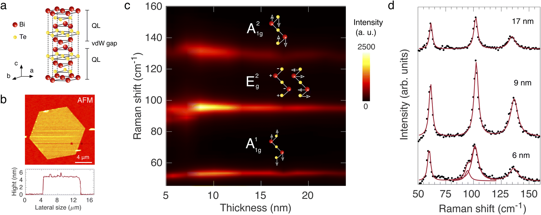 | ||
| Fig. 1 (a) Crystalline structure of Bi2Te3, 1 QL = 0.96 nm. (b) (Top) AFM topography image of hexagonal nanoplatelet with 5 nm QL thickness. Bottom: Line cross-section showing the step height. (c) Intensity map of Raman spectra for a few QLs using excitation laser energy of 1.92 eV, the orange and yellow regions indicate the position of A21g, E2g, and A11g modes. (d) Raman spectra for 6, 9, and 17 nm of crystal thickness withdrawn from (a), the lines are the adjusted curves. | ||
The primitive cell of a QL Bi2Te3 has 5 atoms. Thus group theory predicts three acoustic and 12 optical branches at the center of BZ, Γ (q = 0), and its irreducible representation is Γ = 2Eg ⊕ 2A1g ⊕ 2Eu ⊕ 2A1u, where Eg and Eu modes are twofold degenerates. Only the 2Eg ⊕ 2A1g are Raman active.38,39 To investigate the influence of the number of layers in the vibrational properties of Bi2Te3, we collected the Raman spectrum for samples with thicknesses from 5 up to 24 nm with excitation energy of 1.92 eV. Fig. 1c shows the intensity map of the Raman spectra as a function of thickness, where the colors represent the intensity, yellow for the highest. One can notice three first-order Raman modes located at around 50 cm−1, 100 cm−1 and 135 cm−1 assigned, respectively, as A11g, E2g, and A21g. The A11g and A21g modes correspond to out-of-plane vibrations, while the E2g doubly degenerated mode corresponds to in-plane vibrations (see inset in Fig. 1c). In the A11g mode symmetry, the atoms move in phase while the atoms pairs move in opposite phase for the E22g and A21g modes. We comment that due to the notch filter limit used in our experiment, it was not possible to investigate the Raman modes below 50 cm−1, where the E1g mode (35 cm−1)29 is located. We notice a deviation in these modes' frequency as the layer is reduced. In addition, one can observe an emerged Raman peak of the lower wavenumber shoulder of the E2g mode, as shown in Fig. 1d for a sample with 6 nm QL thickness. This Raman peak is located at around 95 cm−1 and only appears for layers lower than 9 nm. The break of double degenerescence of E2g modes could be associated with increased strain as the number of layers decreases. It is worth of note that all modes present a high intensity for samples of around 10 nm QL thickness. In Fig. 1d, one also observes an asymmetry in the line shape of the A21g mode.
Fig. 2a–c show the Raman frequency position of the A11g, E2g, and A21g modes as a function of the number of layers for the three excitation energies 1.92 eV, 2.41 eV, and 2.54 eV. The frequency position of each mode was extracted from fitting the Raman spectra using the Lorentzian function (see ESI Figures S2–S4†). We can observe that the frequency position of the A21g mode downshifts when increases the number of layers and exhibits a linear behavior for all excitation energies. This dispersion was fitted by straight lines, and the slopes of the number of layers dependence for the A21g modes are −0.21, −0.16 and −0.06 cm−1/L (nm) for, respectively, the 1.92, 2.41 and 2.54 eV laser excitation energies. Here, L (nm) corresponds to the QL thickness. Note that the slope decreases as the excitation energy increases. Intriguingly, the frequency position of the A11g and E2g modes upshift as the number of layers increases, and they become almost constant for thickness above 9 nm; here the lines in these modes are a guide to the eye. The open circles in Fig. 2a are the position of the second peak near E2g due to split. The A11g mode is absent for 2.54 eV excitation laser energy.
 | ||
| Fig. 2 (a–c) The frequency position of A21g, E2g, and A11g modes as a function of QL thickness for excitation laser energies of 1.92, 2.41 and 2.54 eV, respectively. The lines in A11g and E2g modes are a guide to the eye. (d) DFPT calculation of phonons dispersion a long of Γ–Z direction employing the LDA and GGA approximations. | ||
Raman modes are expected to stiffen as an outcome of the confined phonon by the reduction of the number of layers. In this case, the interlayer van der Waals interactions increase the influential restoring forces acting on out-of-plane atoms, thus affecting the frequency of A11g and A21g modes. The shift of in-plane E2g mode may be attributable to long-range Coulomb interlayer interactions.20,41 This finding suggests that the QL stacking also affects the intralayer bonding. To verify this, we performed phonon dispersion calculations based on density functional perturbation theory (DFPT)42 implemented in Quantum Espresso. We examined the phonon dispersion branch of the A11g, E2g, and A21g modes along the Γ–Z direction using the LDA and GGA methods as shown in Fig. 2d. Note that the LDA phonon frequencies are overestimated, while the GGA is underestimated. We observe that the A11g mode redshifts along the Γ–Z direction in agreement with the experimental result, while the A21g mode exhibits an opposite behavior. The reason may be related to the restoring forces as the number of layers decreases. However, further theoretical aid would be required to fully understand this behavior. We also comment that the calculation uncertainty is less than 5 cm−1. The E2g mode does not show dispersion because the calculation was taken only along the out-of-plane direction, thus not enabling us to observe variation for the in-plane mode.
We now examine the intensity enhancement effects of A21g, E2g, and A11g modes for, respectively, 1.92, 2.41, and 2.54 eV laser energies for crystals with 5 to 24 nm QL thickness. Fig. 3a–c show the normalized intensity of the first-order modes, A21g, E2g, and A11g modes, as a function of the crystal's thickness. Two maxima at around 11–12 nm and 18 nm QL thickness are observed for the A21g mode at the 1.92 eV laser energy. These two maxima also appear at the 2.41 and 2.54 eV laser energies, respectively. However, their intensity enhancement is much lower than the 1.92 eV. These two maxima enhancements are also observed for the E2g and A11g modes. Note that for the E2g mode, there is a considerable enhancement for the 2.54 eV, but the A11g mode only exhibits strong enhancement for the 1.92 eV. Besides, notice that the A11g mode is absent for 2.54 eV due to the resonance conditions related to the fact that its electron–phonon matrix elements are small, see Fig. S4.†
 | ||
| Fig. 3 (a–c) Intensity normalized by silicon peak of A21g, E2g, and A11g modes as a function of QL thickness for excitation laser energies of 1.92 eV, 2.41 eV, and 2.54 eV, respectively. (d) The energy difference calculated between van Hove singularities (vHs) from 1 to 12 QLs. | ||
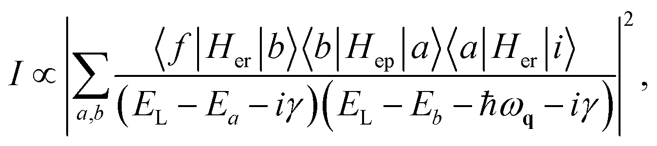
These results are evidence of a resonant Raman scattering being achieved for the Bi2Te3, especially at 1.92 eV laser energy. The mechanism can be described by third-order time-dependent perturbation theory.18,43 The main contribution for the intensity comes from resonance matching between excitation laser energy EL and the separation of vHs in the density of states of the electronic dispersion, i.e., EL = EvHs. Usually, the EL dependence of the Raman intensity of the first-order mode is analyzed. However, in this work, the EL is fixed, and the tuning of the electronic band structure is given by changing the EvHs energy upon the variation in the number of layers. The Raman intensity resonance profile can be expressed by:19
 | (1) |
Therefore, the enhancement observed for 11–12 nm QLs thickness using the excitation laser of 1.92 eV could be due to the matching of EL = EvHs. The electronic states are sensitive to the thickness in the Bi2Te3 system. To verify this, we calculated the density of states of multiple QLs thicknesses. The calculated density of states has van Hove singularities close to the top of the valence band and close to the bottom of the conduction band (see ESI Figures S5 and S6†). Fig. 3d shows the energy differences of the vHs as a function of the QL thickness. One can observe that the gap decreases by the increasing of the number of layers, and it presents a EvHs = 2 eV for 10–12 nm QL thickness, indicating a quasi-matching to EL = 1.92 eV. Therefore, explaining the observed enhancement of all modes.
By inspection of Fig. 1d, one observes that the A21g mode exhibits an asymmetric shape for varying QL thickness at 1.92 eV. To investigate this, we employed the BWF resonance line shape to fit the A21g mode and gain insights into the electron–phonon coupling strength. In short, the BWF resonance describes interactions between the one-phonon scattering process and one-electron excitation from filled to empty valence bands. This results in an asymmetrical line shape produced by the interference between the discrete and continuum scattering mechanisms.20,26,27Fig. 4a shows that the A21g mode has an asymmetric broadening in the line shape when the number of layers increases for the 1.92 eV. The A21g broadening line shape was fitted considering the following expression,
 | (2) |
 | ||
| Fig. 4 (a) BWF line shape fitting and the experimental spectra of A21g mode for 7, 10, 13 nm QL thickness. (b) Fano parameter 1/q dependence on the QL thickness, the line is a guide. | ||
Summary
To summarize, we have investigated a quasi-continuum range of a few quintuple layers of Bi2Te3 synthesized by LPVPD method using AFM and Raman spectroscopy with the aid of DFT calculations. Atomic force microscopy images were used to identify the crystal's thickness. The analyses of the Raman spectra revealed how the main modes (A11g, E2g, and A21g) in Bi2Te3 system behave by the variation of the number of layers and excitation energies. The frequency position of all main modes varies depending on the number of layers. The E2g and A11g mode upshift upon the increasing of the number of layers. On the hand, the A21g mode frequency downshift by the increasing of the number of layers, and with dispersive rates of −0.21, −0.16 and −0.06 cm−1/L (nm) for 1.92, 2.41 and 2.54 eV excitation energies, respectively. The frequency variation of all main modes can be useful to identify the number of Bi2Te3 QL thickness, especially for QL thickness below 9 nm. In addition, we observed a degeneracy break of the E2g modes below 9 nm QL thickness, which might be related to an increase of strain. We observed a resonant Raman condition at 1.92 eV laser energy, where two maxima are observed at about 11 and 18 nm QL thickness. The intensity of all main modes considerably enhances due to matching the excitation energy and a van Hove singularity in the density of states. Furthermore, the electron–phonon coupling strength of the A21g mode was investigated by the BWF resonance line shape. The Fano parameter (1/q) increases from 5 to 24 QLs thickness, indicating that the electron–phonon coupling is robust for the thick layers. This electron–phonon coupling enhancement also contributes to the resonance Raman scattering. These results are a complete picture of the electron and phonon properties and their dependency on the numbers of layers of the Bi2Te3 systems.Author contributions
V. C., B. R. C., and M. T. conceived the idea and wrote the manuscript with inputs from all authors. V. C. carried out the sample synthesis and characterization. S. H. S worked on the data analysis. L. S. and P. M. V. did the first principle calculations. Finally, all the authors discussed the results and commented on and revised the manuscript.Conflicts of interest
The authors declare no competing financial interest.Acknowledgements
V. C. acknowledges the CNPq and FAPERJ grants numbers 429773/2018-8, 304144/2018-5 end E-26/010.000980/2019. B. R. C., L. S., P. V. acknowledges the financial support from the Brazilian agencies CAPES and CNPq. M. T. acknowledges the Air Force Office of Scientific Research grant number 158198. We acknowledge Simin Feng for the aid in the AFM measurements.Notes and references
- C. Chen, Z. Xie, Y. Feng, H. Yi, A. Liang, S. He, D. Mou, J. He, Y. Peng, X. Liu, Y. Liu, L. Zhao, G. Liu, X. Dong, J. Zhang, L. Yu, X. Wang, Q. Peng, Z. Wang, S. Zhang, F. Yang, C. Chen, Z. Xu and X. J. Zhou, Sci. Rep., 2013, 3, 2411 CrossRef PubMed.
- H. Zhang, C.-X. Liu, X.-L. Qi, X. Dai, Z. Fang and S.-C. Zhang, Nat. Phys., 2009, 5, 438–442 Search PubMed.
- M. Z. Hasan and C. L. Kane, Rev. Mod. Phys., 2010, 82, 3045–3067 CrossRef CAS.
- M. S. Bahramy, P. D. C. King, a. de la Torre, J. Chang, M. Shi, L. Patthey, G. Balakrishnan, P. Hofmann, R. Arita, N. Nagaosa and F. Baumberger, Nat. Commun., 2012, 3, 1157–1159 CrossRef PubMed.
- L. Fu and C. L. Kane, Phys. Rev. Lett., 2008, 100, 096407 CrossRef PubMed.
- Y. Xu, I. Miotkowski, C. Liu, J. Tian, H. Nam, N. Alidoust, J. Hu, C.-K. Shih, M. Z. Hasan and Y. P. Chen, Nat. Phys., 2014, 10, 956–963 Search PubMed.
- Y. L. Chen, J. G. Analytis, J.-H. Chu, Z. K. Liu, S.-K. Mo, X. L. Qi, H. J. Zhang, D. H. Lu, X. Dai, Z. Fang, S. C. Zhang, I. R. Fisher, Z. Hussain and Z.-X. Shen, Science, 2009, 325, 178–181 CrossRef CAS PubMed.
- D. Teweldebrhan, V. Goyal and A. a. Balandin, Nano Lett., 2010, 10, 1209–1218 CrossRef CAS PubMed.
- G. Wang, X. G. Zhu, Y. Y. Sun, Y. Y. Li, T. Zhang, J. Wen, X. Chen, K. He, L. L. Wang, X. C. Ma, J. F. Jia, S. B. Zhang and Q. K. Xue, Adv. Mater., 2011, 23, 2929–2932 CrossRef CAS PubMed.
- Y.-Y. Li, G. Wang, X.-G. Zhu, M.-H. Liu, C. Ye, X. Chen, Y.-Y. Wang, K. He, L.-L. Wang, X.-C. Ma, H.-J. Zhang, X. Dai, Z. Fang, X.-C. Xie, Y. Liu, X.-L. Qi, J.-F. Jia, S.-C. Zhang and Q.-K. Xue, Adv. Mater., 2010, 22, 4002–4007 CrossRef CAS PubMed.
- G. Zhang, H. Qin, J. Teng, J. Guo, Q. Guo, X. Dai, Z. Fang and K. Wu, Appl. Phys. Lett., 2009, 95, 53114 CrossRef.
- C. X. Liu, H. Zhang, B. Yan, X. L. Qi, T. Frauenheim, X. Dai, Z. Fang and S. C. Zhang, Phys. Rev. B, 2010, 81, 2–5 Search PubMed.
- K. Hoefer, C. Becker, D. Rata, J. Swanson, P. Thalmeier and L. H. Tjeng, Proc. Natl. Acad. Sci. U. S. A., 2014, 111, 14979–14984 CrossRef CAS PubMed.
- C. Li, T. Winzer, A. Walsh, B. Yan, C. Stampfl and A. Soon, Phys. Rev. B, 2014, 90, 1–7 Search PubMed.
- L. Seixas, L. B. Abdalla, T. M. Schmidt, A. Fazzio and R. H. Miwa, J. Appl. Phys., 2013, 113, 2011–2015 CrossRef.
- I. Garate, Phys. Rev. Lett., 2013, 110, 046402 CrossRef PubMed.
- K. Saha and I. Garate, Phys. Rev. B: Condens. Matter Mater. Phys., 2014, 89, 205103 CrossRef.
- A. Jorio, R. Saito, G. Dresselhaus and M. S. Dresselhaus, Raman Spectroscopy in Graphene Related Systems, Wiley-VCH, Berlin, 2011 Search PubMed.
- V. Carozo, C. M. Almeida, B. Fragneaud, P. M. Bedê, M. V. O. Moutinho, J. Ribeiro-Soares, N. F. Andrade, A. G. Souza Filho, M. J. S. Matos, B. Wang, M. Terrones, R. B. Capaz, A. Jorio, C. A. Achete and L. G. Cançado, Phys. Rev. B: Condens. Matter Mater. Phys., 2013, 88, 085401 CrossRef.
- J. Zhang, Z. Peng, A. Soni, Y. Zhao, Y. Xiong, B. Peng, J. Wang, M. S. Dresselhaus and Q. Xiong, Nano Lett., 2011, 11, 2407–2414 CrossRef CAS PubMed.
- X.-L. Qi and S.-C. Zhang, Rev. Mod. Phys., 2011, 83, 1057–1110 CrossRef CAS.
- Y. Xia, D. Qian, D. Hsieh, L. Wray, A. Pal, H. Lin, A. Bansil, D. Grauer, Y. S. Hor, R. J. Cava and M. Z. Hasan, Nat. Phys., 2009, 5, 18 Search PubMed.
- K. He, Y. Zhang, K. He, C.-Z. Chang, C.-L. Song, L.-L. Wang, X. Chen, J.-F. Jia, Z. Fang, X. Dai, W.-Y. Shan, S.-Q. Shen, Q. Niu, X.-L. Qi, S.-C. Zhang, X.-C. Ma and Q.-K. Xue, Nat. Phys., 2010, 6, 584–588 Search PubMed.
- G. Hao, X. Qi, Y. Liu, Z. Huang, H. Li, K. Huang, J. Li, L. Yang and J. Zhong, J. Appl. Phys., 2012, 111, 1–6 Search PubMed.
- D. Kong, W. Dang, J. J. Cha, H. Li, S. Meister, H. Peng, Z. Liu and Y. Cui, Nano Lett., 2010, 10, 2245–2250 CrossRef CAS PubMed.
- U. Fano, Phys. Rev., 1961, 124, 1866–1878 CrossRef CAS.
- S. D. Brown, A. Jorio, P. Corio, M. S. Dresselhaus, G. Dresselhaus, R. Saito and K. Kneipp, Phys. Rev. B: Condens. Matter Mater. Phys., 2001, 63, 1–8 Search PubMed.
- R. He, Z. Wang, R. L. J. Qiu, C. Delaney, B. Beck, T. E. Kidd, C. C. Chancey and X. P. a. Gao, Nanotechnology, 2012, 23, 455703 CrossRef PubMed.
- Y. Zhao, X. Luo, J. Zhang, J. Wu, X. Bai, M. Wang, J. Jia, H. Peng, Z. Liu, S. Y. Quek and Q. Xiong, Phys. Rev. B: Condens. Matter Mater. Phys., 2014, 90, 245428 CrossRef.
- S. Xu, Y. Han, X. Chen, Z. Wu, L. Wang, T. Han, W. Ye, H. Lu, G. Long, Y. Wu, J. Lin, Y. Cai, K. M. Ho, Y. He and N. Wang, Nano Lett., 2015, 15, 2645 CrossRef CAS PubMed.
- Y. Jiang, X. Zhang, Y. Wang, N. Wang, D. West, S. Zhang and Z. Zhang, Nano Lett., 2015, 15, 3147–3152 CrossRef CAS PubMed.
- P. Giannozzi, O. Andreussi, T. Brumme, O. Bunau, M. B. Nardelli, M. Calandra, R. Car, C. Cavazzoni, D. Ceresoli, M. Cococcioni, N. Colonna, I. Carnimeo, A. D. Corso, S. de Gironcoli, P. Delugas, R. A. DiStasio, A. Ferretti, A. Floris, G. Fratesi, G. Fugallo, R. Gebauer, U. Gerstmann, F. Giustino, T. Gorni, J. Jia, M. Kawamura, H.-Y. Ko, A. Kokalj, E. Küçükbenli, M. Lazzeri, M. Marsili, N. Marzari, F. Mauri, N. L. Nguyen, H.-V. Nguyen, A. Otero-de-la Roza, L. Paulatto, S. Poncé, D. Rocca, R. Sabatini, B. Santra, M. Schlipf, A. P. Seitsonen, A. Smogunov, I. Timrov, T. Thonhauser, P. Umari, N. Vast, X. Wu and S. Baroni, J. Phys.: Condens. Matter, 2017, 29, 465901 CrossRef CAS PubMed.
- P. E. Blöchl, Phys. Rev. B: Condens. Matter Mater. Phys., 1994, 50, 17953–17979 CrossRef PubMed.
- J. P. Perdew and A. Zunger, Phys. Rev. B: Condens. Matter Mater. Phys., 1981, 23, 5048–5079 CrossRef CAS.
- J. P. Perdew, K. Burke and M. Ernzerhof, Phys. Rev. Lett., 1996, 77, 3865–3868 CrossRef CAS PubMed.
- L. Fu and C. L. Kane, Phys. Rev. B: Condens. Matter Mater. Phys., 2007, 76, 045302 CrossRef.
- Y.-x. Yuan, L. Ling, X.-y. Wang, M. Wang, R.-a. Gu and J.-l. Yao, J. Raman Spectrosc., 2007, 38, 1280–1287 CrossRef CAS.
- W. Richter, H. Köhler and C. R. Becker, Phys. Status Solidi B, 1977, 84, 619–628 CrossRef CAS.
- J. O. Jenkins, J. A. Rayne and R. W. Ure, Phys. Rev. B: Condens. Matter Mater. Phys., 1972, 6, 1609 CrossRef.
- B. Y. Yavorsky, N. F. Hinsche, I. Mertig and P. Zahn, Phys. Rev. B: Condens. Matter Mater. Phys., 2011, 84, 165208 CrossRef.
- C. Lee, H. Yan, L. E. Brus, T. F. Heinz, J. Hone and S. Ryu, ACS Nano, 2010, 4, 2695–2700 CrossRef CAS PubMed.
- S. Baroni, S. de Gironcoli, A. Dal Corso and P. Giannozzi, Rev. Mod. Phys., 2001, 73, 515–562 CrossRef CAS.
- R. Saito, M. Hofmann, G. Dresselhaus, A. Jorio and M. S. Dresselhaus, Adv. Phys., 2011, 60, 413–550 CrossRef CAS.
- R. Gupta, Q. Xiong, C. K. Adu, U. J. Kim and P. C. Eklund, Nano Lett., 2003, 3, 627–631 CrossRef CAS.
- C. Attaccalite, L. Wirtz, M. Lazzeri, F. Mauri and A. Rubio, Nano Lett., 2010, 10, 1172–1176 CrossRef CAS PubMed.
Footnote |
| † Electronic supplementary information (ESI) available. See DOI: https://doi.org/10.1039/d3na00585b |
| This journal is © The Royal Society of Chemistry 2023 |