DOI:
10.1039/D3NA00565H
(Paper)
Nanoscale Adv., 2023,
5, 6858-6869
Ultra-broadband near-perfect metamaterial absorber for photovoltaic applications†
Received
27th July 2023
, Accepted 15th October 2023
First published on 16th October 2023
Abstract
An ingenious double-grating metamaterial-based ultrathin-broadband absorber consisting of AlGaAs–Ge–GaAs on a titanium film operating in the visible to infrared wavelength was designed in this work. This structure is capable of overcoming the Shockley–Queisser (SQ) limit and the tunneling junction effect of tandem solar cells. Our comprehensive study revealed the structure's absorption mechanism using the finite-difference time-domain (FDTD) technique, which exhibited excellent short-circuit current density and high absorption. Our proposed ultrathin structure of 410 nm thickness provided a high average absorption of 82.2% and 99.7% under unpolarized and TM-polarized light for a wavelength range of 450–2000 nm, respectively. Additionally, we observed high incidence angle tolerability under the plane wave and thermal stability over time for our proposed grating structure. The performance analysis of our proposed structure as an absorber layer of a solar cell revealed its high power conversion efficiency (PCE) of 31.7% with an excellent short-circuit current density of 47.1 mA cm−2 for AM 1.5 G solar irradiance. The double-grating metamaterial absorber structure has enormous potential for diverse applications such as solar harvesting, thermoelectric generation, and photodetection.
1 Introduction
Due to limited fossil fuels in recent years, humans are currently experiencing an energy crisis. One of the most promising candidates to alleviate this energy shortage is renewable energy, specifically solar energy. Absorbers absorb incident light and convert it to electrical energy. Broadband and narrowband light absorbers are the two ramifications based on the spectral bandwidth of light. Narrowband absorbers can be applicable for sensors, resonators, and modulators in the range of both visible and infrared regions.1–6 However, broadband absorbers are essential for photovoltaic cells,7,8 photodetectors,9 and thermal emitters.10,11 Over the years, broadband photon absorbers with various structures such as nanowires,12 nanopillars,13 triangular and pyramid gratings,14 nanocones,15 plasmonic nanostructures,16 and nanoholes17 have been reported theoretically and experimentally for harvesting solar energy. Most of the reported research studies mainly focused on absorbing the visible light spectrum; however, approximately half of the sunlight that reaches the surface of the Earth contains infrared radiation. Moreover, the light of longer wavelengths must be trapped so that we can enhance the efficiency of the solar cell device. Though numerous tandem solar cells have been reported by utilizing various bands of the electromagnetic (EM) spectrum, they are typically expensive and complex to manufacture. Therefore, there is scope for research to design an absorber structure that can utilize a wide range of absorption from visible to infrared regions.
Since the discovery of metamaterials in 1967 by V. G. Veselago, a huge research interest has developed in controlling and manipulating EM waves using artificially designed subwavelength structures.18 Over the last few decades, metamaterial-based devices have been getting considerable attention because of their numerous applications, including antenna systems,19 ultra-sensitive sensing,20 EM cloaking,21 refractive index engineering,22 and optoelectronic devices.23,24 Due to the high demand for highly sensitive image sensors and energy harvesting, researchers are relentlessly searching for perfect light-trapping metamaterial structures. Various simple and complex nanostructures, such as metamaterials, tandem solar cells, nanowires, incorporating plasmonic nanoparticles, gratings, resonators, and metal–insulator–metal (MIM), absorbers with good absorbance capacities have been reported to harvest solar energy. For instance, silicon (Si) solar cells cover ∼80% market of total solar cells due to their matured fabrication technology; however, the PCE is poor. Incorporating TiN, an alternative plasmonic material, nanoparticles in the absorber increased the absorption power from ∼19% to ∼75%.25 However, the absorbed power can be improved, and that structure operated in the 400–1000 nm wavelength range only. Nanowire structures can trap photons;26 however, the obtained PCE was only ∼8%. Wang et al. reported an ultra-broadband nanowire structure comprising MIM layers.27 They obtained an average absorption of ∼90% in the wavelength range from 0.2 to 7 μm; however, MIM solar cells have instability problems, which resulted in poor efficiency, and open circuit voltage cannot overcome half of the energy bandgap.28,29 Most importantly, they conducted optical numerical analysis under polarized light only, whereas sunlight has the nature of an unpolarized wave. Trapezoid plasmonic nano-resonators, a dielectric grating array of sandwiched nickel films, and quadrilateral truncated GaAs cones obtained a high absorption of around 85% in the visible wavelength regime.8,30,31 Perhaps the short wavelength coverage limited the proposed structures. Lei et al. proposed a metamaterial structure comprising titanium-silica cubes to obtain ultra-broadband absorption in the visible to near-infrared wavelength.32 Wang et al. proposed a simple gold rectangular-shaped metamaterial light absorber in the terahertz (THz) frequency regime;33 however, absorption decreased due to its asymmetric nature. This drawback might be resolved using a ring resonator structure.34 However, the PCE will be poor, as the solar irradiance is minimal in the THz region. Tandem solar cells can overcome the SQ limit, which is impossible with a single bandgap material; however, these cells are difficult to design due to tunneling junctions.35 Most of the light absorber nanostructures had limited and specific advantages; thus, there is vast scope for designing flexible ultra-broadband and ultrathin absorbers with excellent power conversion efficiency. Moreover, the absorption characteristics of single-grating structures were studied;8,14 however, the optical, thermal, and electrical properties of engineered double-grating structures are yet to be explored. As different complex grating structures can be grown experimentally,36–38 the optical characteristics and performance analysis of metamaterial-based double-grating structures will open the door for various optoelectronic and metrology applications.
In this work, we proposed an ingenious double-grating metamaterial-based ultrathin-broadband absorber comprising the semiconductor materials of aluminum gallium arsenide (AlGaAs)–germanium (Ge)–gallium arsenide (GaAs) on a refractory metal titanium (Ti) film. Our proposed structure overcame the SQ limit and did not require a tunneling junction like a tandem solar cell. We optimized the structural parameters of the proposed structure and evaluated the optical performance using the FDTD method. Besides studying the effects of structural parameters, the origin underlying the broadband light-trapping phenomenon was explained in detail. Electrical simulations exhibited a high PCE due to broadband light absorption through our proposed structure. In addition, the thermal stability under a steady state and the transient response of the proposed double-grating metamaterial structure were analyzed to observe how light absorption affected the structure's temperature. Moreover, we compared the performance of the proposed structure not only with the bare double-grating structures but also with the recently demonstrated metamaterial-based broadband absorbers. In addition to numerical analysis, this study discusses the practical issues of experimentally realizing these structures so that they can be utilized as the active region of photovoltaic devices.
2 Device design and methodology
A vertically stacked periodic array of different materials was designed to observe perfect absorption in a wide optical wavelength range from visible to infrared regions. Fig. 1(a) depicts the proposed double-grating metamaterial absorber structure. The proposed structure was periodic in the x-direction and infinitely long in the y-direction. A Ti slab was employed to reflect back light into the structure, enhancing light absorption and reducing transmission through the structure. A negligible amount of transmission through the structure was observed while the thickness of the Ti slab, tTi, of 200 nm was utilized. On the top of the Ti slab, an ultra-thin GaAs layer with a thickness, tGaAs, of 30 nm was used to increase light absorption in the structure. The width, k, and thickness, tGe, of Ge were 210 nm and 120 nm, respectively, while the periodicity of the Ge grating, p, was set to be 420 nm. Two rectangular bars of AlGaAs were positioned at the edges of the Ge surface, as can be seen in Fig. 1. It gave rise to a double-grating structure. The width, q, and thickness, tAlGaAs, of the AlGaAs were set to be 75 nm and 60 nm, respectively. All the parameters were taken optimally by conducting numerical analysis. We provided a detailed discussion of how the parameters were optimized in a later section. A lateral metal contact will be formed with the AlGaAs layer to connect with an external circuit. The complex refractive indices of Ti, GaAs, and Ge were obtained from Palik et al.39 We adopted the refractive index and extinction coefficient data of AlGaAs as a function of wavelength from Adachi et al.,40 where the contribution of Al was 30%. The refractive indices and extinction coefficients of GaAs, Ge, AlGaAs, and Ti are presented in Fig. S1 of the ESI.† The lattice parameters of AlGaAs, Ge, and GaAs were 5.6556 Å, 5.6578 Å, and 5.6622 Å, respectively. As the lattice mismatch between the layers of our proposed absorber was extremely low (<0.1%), there will be negligible strain and, consequently, minimal interface defects.
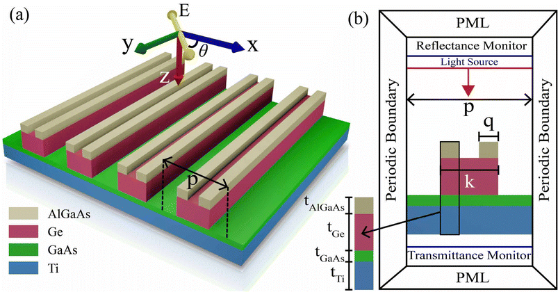 |
| | Fig. 1 (a) Illustration of a double-grating-based metamaterial absorber. A plane light wave was incident on the structure with an electric field along the z-direction where θ is the polarization angle. (b) Cross-sectional view of the xz plane of our proposed absorber, where p = 420 nm, tTi = 200 nm, tGaAs = 30 nm, k = 210 nm, tGe = 120 nm, q = 75 nm, and tAlGaAs = 60 nm. | |
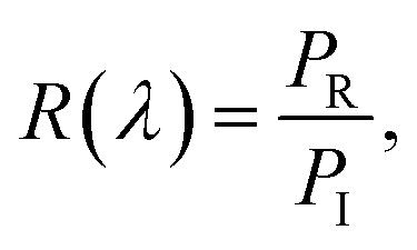
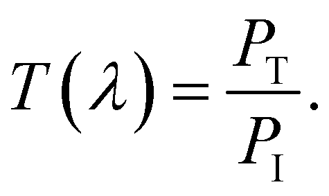
We performed numerical calculations using the FDTD method to study the optical properties of our proposed structure. In order to minimize computational space, we conducted a 2D FDTD simulation because the structure can be realized as infinitely long in the y-direction. The periodic boundary conditions were utilized in the positive and negative x-directions. 12 perfectly matched steep angle layers were used in the z-direction to absorb the reflected and transmitted light from the simulation region. Moreover, we performed the 3D FDTD simulation and compared it with the absorption spectra of the 2D FDTD simulation. We found the same absorption result for our metamaterial structure in both cases. The detailed simulation setup is shown in Fig. 1(b). A transverse magnetic (TM), transverse electric (TE), and unpolarized plane wave were employed on the top surface of the structure along the z-direction. We used a mesh size of 3 nm in our simulations. We employed power monitors to enumerate transmitted and reflected lights below the metamaterial structure and above the plane wave, respectively, as depicted in Fig. 1(b). Power monitors were used in the wavelength domains to calculate field power in some spatial regions. Monitors recorded reflectance and transmittance as follows,
| |  | (1) |
| |  | (2) |
Here,
λ is the wavelength of the plane wave, and
R(
λ) and
T(
λ) are the reflectance and transmittance of the structure as a function of wavelength.
PR,
PT, and
PI are the powers of reflected, transmitted, and incident plane waves, respectively. The absorbance of the metamaterial structure,
A(
λ), was calculated by,
| | | A(λ) = 1 − R(λ) − T(λ). | (3) |
The temperature was set to be 300 K, and the size of the simulation region was equal to the periodicity of the metamaterial structure for all simulations. Moreover, the thermal analysis of our proposed structure under steady and transient states was performed by calculating the 3D heat transfer equation. In these analyses, we utilized our proposed structure's heat generation profile from the FDTD simulations. A table of the utilized material's thermal properties is given in Table S1 of the ESI.†
The current density (J)–voltage (V) curve of the proposed double-grating metamaterial structure was calculated by solving the continuity and Poisson's equations using SCAPS-1D open-source software.41 Here, the absorption characteristic under unpolarized incident light was utilized for comparing theoretical and simulated short circuit current (JSC). The AlGaAs, Ge, and GaAs layers were p-type doped, intrinsic, and n-type doped, respectively. The bandgap energies of AlGaAs, Ge, and GaAs layers were considered to be 1.58 eV, 0.7 eV, and 1.42 eV, respectively. The metalwork function of the Ti back reflector was set to be 4.33 eV. The trapping states and recombination centers reduced the performance of solar cells. Here, the total recombination defect density of AlGaAs, Ge, and GaAs was considered to be 8 × 1014 cm−3, 1 × 1016 cm−3, and 1 × 1016 cm−3, respectively. A table of the utilized material's electrical properties is provided in Table S2 of the ESI.† Moreover, we studied the effects of the different shunt (Rsh) and series (Rs) resistances using the parametric sweep.
3 Results and discussion
3.1 Device physics
To find the physical origin of the ultra-broadband absorber, we separately analyzed the effects of different materials in our proposed double-grating metamaterial structure for TM polarized incident light. AlGaAs and GaAs have larger band gaps than Ge and show poor light absorption in longer wavelength (>1000 nm) regimes. Conversely, Ge, a low bandgap material, shows good light absorption in the longer wavelength, as depicted in Fig. 2(a). However, Ge's bandgap is far from the optimum bandgap, which provides poor PCE. Moreover, the homojunction structures have problems overcoming the SQ limit. Thus, a structure can achieve broadband and perfect light absorption by comprising these materials. In our proposed structure, AlGaAs contributed to trapping the shorter wavelengths (∼visible range) of light due to their sufficient thickness. In contrast, the Ge and GaAs layers absorbed medium wavelength photons (∼700–1000 nm) and back-reflected longer wavelength photons from Ti as they traversed a longer path, as shown in Fig. 2(b). The GaAs layer acted as a light absorption booster (see Fig. S2 of the ESI†). The impact of the Ti back-reflector layer is evident from the absorption spectra shown in Fig. S2 of the ESI.† The light beyond the wavelength of 750 nm was transmitted through the structure without the Ti slab. The reduction of light absorption for the slab and single grating structure was the main reason to propose a double-grating metamaterial structure (see Fig. S2 of the ESI†). Multimedia file 1† illustrates the absorption mechanism of our proposed double-grating metamaterial structure. Different layers trap light in the wide wavelength range from the visible to the infrared regime by reducing reflection from the proposed structure. As Ti acted as a complete back-reflector in our proposed double-grating structure, we observed negligible transmission through the structure. The resultant light absorption of different materials for our proposed double-grating structure is illustrated in Fig. 2(c). Average absorption, Aavg, of 96.5% with a peak absorption of 99.9% at 610 nm was calculated over the wavelength range from 450 to 3000 nm. Our proposed double-grating structure exhibited a high Aavg of 98.2% in a wide wavelength range from 450 to 2000 nm. Here, Aavg was enumerated using,15| | 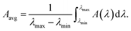 | (4) |
Here, λmax and λmin are our studied range's maximum and minimum wavelengths. Additionally, we calculated the Aavg for our proposed structure under unpolarized light, i.e., AM 1.5 G solar irradiance. We obtained an Aavg of 87.0% in the wavelength range from 450 to 3000 nm with a peak absorption of 99.7% at 725 nm. We obtained a high Aavg of 82.2% in the wavelength range from 450 to 2000 nm for our proposed structure.
 |
| | Fig. 2 (a) Numerically analyzed absorption spectra under TM-polarized light using different materials in double-grating structures. Insets represent the structural unit cells of corresponding absorption data. AlGaAs, Ge, GaAs, and metamaterial double-grating structures are denoted as structures I, II, III, and IV, respectively. (b) The absorption and reflectance contribution in different layers of the proposed metamaterial double-grating structure. The origin of broadband absorption spectra can also be visualized. (c) Absorption, reflectance, and transmittance spectra of the metamaterial absorber under TM-polarized light. The average absorption over a bandwidth of 1550 nm and 2550 nm is 98.2% and 96.5%, respectively. The peak absorption is 99.9% at 610 nm. | |
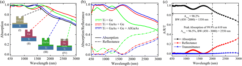
To further investigate the physical mechanism of the proposed double-grating metamaterial structure, the spatial xz cross-section of current density (|J|), electric field (|E|2), and magnetic field (|H|2) distributions of the TM polarized light with a normal incidence were demonstrated at different wavelengths of 455 nm, 790 nm, 1342 nm, and 1818 nm, as illustrated in Fig. 3. The exact location of the light absorption was identified by analyzing current density distributions in the structure. As depicted in Fig. 3(a) and (b), shorter and medium wavelength absorption occurred at AlGaAs and Ge–GaAs layers, respectively. In contrast, back-reflected light from Ti contributed to the origin of longer wavelength absorption, as shown in Fig. 3(c) and (d). However, the reason behind decreasing absorption at longer wavelengths could also be comprehended by observing the reduction of reflected photons in the Ge layer. As depicted from Fig. 3(e)–(h), the electric field is strongly confined on both sides of the gratings; we can infer that the surface plasmons were excited within the structure. The structure absorbed the electric field of light, which can be visualized by the dark color region of the structure. In addition, the incoming light was coupled into the air spacing between adjacent periodic arrays, and the edges of the gratings demonstrated the emergence of the strongest electric field distributions. Below a wavelength of 1000 nm, relatively weak magnetic field distributions were observed in the proposed metamaterial grating structure due to inadequate photons at the interface of GaAs–Ti, which indicated the dominant role of absorption as apparent from the electric field distributions illustrated in Fig. 3(i) and (j). In contrast, the magnetic field distributions beyond the wavelength of 1000 nm were confined in the GaAs layer, especially at the interface between Ti and GaAs layers, as can be seen in Fig. 3(k) and (l). The weak magnetic field energy at the Ti–GaAs interface suggested that the electric field dominated the absorption band. These indicated the excitation of propagating surface plasmon (SP) mode at the interface between Ti and GaAs layers.
 |
| | Fig. 3 Spatial xz-current density (|J|) (a–d), -electric field (|E|2) (e–h), and -magnetic field (|H|2) (i–l) distributions for a unit cell under TM-polarized light at wavelengths of 455 nm, 790 nm, 1342 nm, and 1818 nm. The dotted lines depict the proposed double grating absorber structure. | |
3.2 Effects of geometrical parameters on absorption
We investigated the effects of structural parameters on absorption performance and utilized the optimized parameters for our proposed double-grating metamaterial structure. Fig. 4 illustrates the effect of the geometrical parameters on the absorption spectra. Dips appeared in the absorption spectra when k and q were increased, as seen in Fig. 4(a) and (b). In both cases, the performance parameter of an absorber, Aavg, reduced while reflection increased from the structure. The near-perfect absorption was achieved for k = ∼210 nm and q = ∼75 nm. Hence, k and q were set to these values for further simulations of our proposed double-grating structure. Varying p from 420 nm reduced the Aavg with increasing the reflection from the structure, which behaved like a continuous film stack structure.32 Therefore, we adopted 420 nm as the optimal periodicity of our structure, as presented in Fig. 4(c). Additionally, we analyzed the absorption spectra of our proposed structure for varying the thicknesses of Ge, AlGaAs, and GaAs layers. The impact of the tGe can be seen from Fig. 4(d) where the absorption spectra gradually redshifted while thickness was increasing. This is mainly due to the increased effective path length.32 As our goal was to achieve ultra-broadband near-perfect absorption utilizing an ultra-thin structure, we set the value of tGe to be 120 nm for our work. As the thickness variation of AlGaAs did not influence the absorption spectra as depicted in Fig. 4(e), we considered a tAlGaAs of 60 nm for our study. The effect of the tGaAs is shown in Fig. 4(f). The absorption was redshifted and reduced in the visible wavelength region. As nearly 50% of solar irradiance with the peak is in the visible wavelength region, we should capture light as much as possible from the visible region. Therefore, a tGaAs of 30 nm was set.
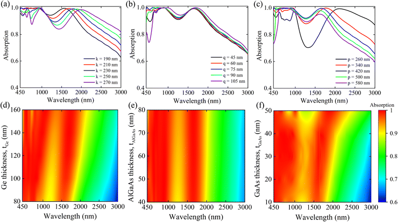 |
| | Fig. 4 Illustration of effects of the geometric parameters (a) k, (b) q, (c) p, (d) tGe, (e) tAlGaAs, and (f) tGaAs on absorption performances for TM-polarized light. | |
3.3 Effect of incident light polarization
The polarization-independent absorption is desired for good absorbers. We performed optical measurements at normal incidence for different polarization angles. The proposed structure can maintain a strong average absorption up to a polarization angle of 60°, as seen in Fig. 5(a). Moreover, the double-grating metamaterial structure split the absorption spectrum due to the asymmetrical nature of the structure and exhibited a spectral broadening at the longer wavelength range above the polarization angle of 60°.
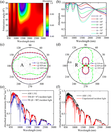 |
| | Fig. 5 (a) Evolution of polarization sensitivity in absorption spectra at different polarization angles. (b) Absorption spectra for the double-grating metamaterial structure at different θ. The polar plot of normalized (c) absorption and (d) reflectance at wavelengths of 518 nm, 829 nm, and 1432 nm. ASI under AM 1.5 G for (e) TM and TE polarization and (f) unpolarized incident light. The ASI of the proposed structure under TM-polarized light follows the ASI of AM 1.5 G solar irradiance, and the converse case is applicable for TE-polarized light. Moreover, the electric field distributions of TM, TE, and unpolarized light demonstrate similar trends (see Multimedia file 2†). | |
In particular, the absorption window can include the irradiation wave for spectral broadening in the longer wavelength range and provide a weak absorption band at around 1432 nm.42 The TE-polarized incident light on the metamaterial double-grating structure had a broader bandwidth than the TM-polarized incident light. Therefore, the proposed metamaterial double-grating structure exhibited many weak absorption dips, especially around the wavelength of 1432 nm for TE-polarized light (θ = 90°), as illustrated in Fig. 5(b). The proposed structure under TM-polarized light (θ = 0°) exhibited higher Aavg than TE-polarized light (θ = 90°) due to the low band gap. Absorption decreased at three dips of 518, 829, and 1432 nm wavelengths while we increased θ. However, absorption beyond ∼2250 nm increased with increasing θ. The band gap of the double-grating metamaterial structure under TM- and TE-polarized incident light can be obtained using the Tauc plot from absorption spectra (see Fig. S3 of the ESI†).
For better understanding, the polar plots of normalized absorbance and reflectance spectra at 518, 829, and 1432 nm wavelengths are shown in Fig. 5(c) and (d), respectively. Here, we observed perfect absorption for TM-polarization light (θ = 0°), reducing reflection from the structure. For TE-polarized incident light, the proposed structure exhibited the most reflection, which is the main reason for absorption reduction and the appearance of the polarization dependence absorption dip at 518, 829, and 1432 nm wavelengths. We calculated absorbed spectral intensity (ASI) for AM 1.5 G solar irradiance for TM, TE, and unpolarized light, as illustrated in Fig. 5(e) and (f). As the structure exhibited near-perfect broadband absorption for TM polarization, the ASI of TM polarization light nearly followed the ASI of AM 1.5 G solar irradiance, as shown in Fig. 5(e). The ASI curve for TE-polarization light did not follow the ASI of AM 1.5 G due to weak absorption. As sunlight has an unpolarized nature, it is a good practice to study the ASI curve with unpolarized light (see Fig. 5(f)). The absorption, reflectance, and transmittance spectra of unpolarized light are provided in Fig. S4 of the ESI.† The lost and gain energy spectra of TM, TE, and unpolarized light under AM 1.5 G solar light are given in Fig. S5 of the ESI.†
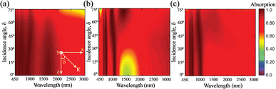
Additionally, near-perfect absorption with an insensitive incidence angle, δ, is desired for good absorbers. The effect of oblique incidence angles on absorption spectra for TM, TE, and unpolarized lights is given in Fig. 6. The metamaterial double-grating structure can maintain a high Aavg of 90% up to an incidence angle of 65° for the TM polarized incident light in the wavelength range between 450 nm and 3000 nm. In contrast, the Aavg increased gradually with increasing the incidence angle of TE polarized light, as depicted in Fig. 6(b). The proposed structure exhibited an absorption dip at around 1500 nm under an incidence angle of 25°. As the proposed structure achieved high absorption for the shorter incidence angle range of TM-polarized light and high absorption for the longer incidence angle range of TE-polarized light, we obtained strong absorption for the 0° to 75° incidence angle range under unpolarized light, as depicted in Fig. 6(c). Moreover, line plots are provided for the effects of different incidence angles in Fig. S6 of the ESI.† Thus, the designed double-grating metamaterial absorber had an excellent incidence-angle insensitivity compared to those in previously reported studies.32,43,44 We provided a detailed comparative analysis in the Comparative analysis section.
 |
| | Fig. 6 Color plot of calculated absorption spectra for different incidence angles for (a) TM, (b) TE, and (c) unpolarized light. The inset of (a) depicts the incidence angle, δ, of a TM-polarized plane wave. | |
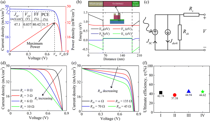
3.4 Photovoltaic performance analysis
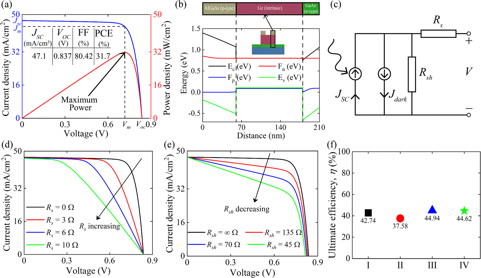
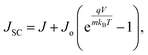
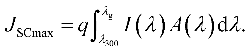
To evaluate the photovoltaic performance of the double-grating structures I, II, III, and IV, the short-circuit current density (JSC), Aavg, light absorption efficiency (LAE), ultimate efficiency (η), current density–voltage (J–V), and power density–voltage (P–V) were calculated under AM 1.5 G solar illumination. The JSCmax is the maximum current density under zero voltage conditions, which can be enumerated theoretically using,29| |  | (5) |
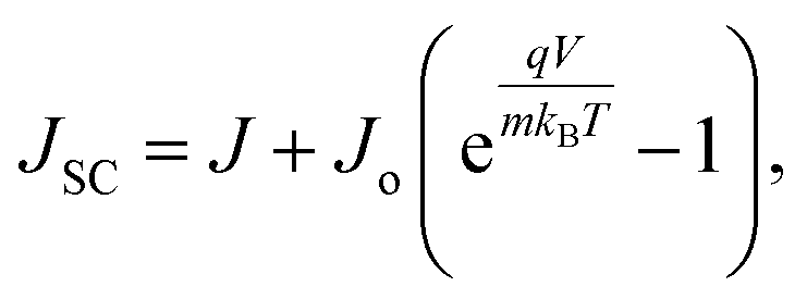
Here, λ300, I(λ), and q denote the minimum wavelength of the solar spectrum, AM 1.5 G solar spectrum irradiance, and the charge of an electron, respectively. We used the wavelength corresponding to the semiconductor band gap as λg for GaAs, Ge, and AlGaAs. The band gaps of the metamaterial structure under TM, TE, and unpolarized lights were obtained by using the Tauc plot45 (see Fig. S3 of the ESI†). High JSCmaxs of 69.4 and 67.0 mA cm−2 were obtained for structures II and IV under unpolarized incident light, respectively. Two assumptions were taken into account in our theoretical study: each photon was absorbed with energies greater than the bandgap and neglected the effect of contacts. However, JSCmax and open circuit voltage, VOC, are meaningless in the pragmatic device world without a close circuit system. Therefore, load or resistance is required to evaluate the performance of a solar absorber, which is called the J–V characteristic plot. Fig. 7(a) depicts the J–V and P–V characteristic curves under unpolarized incident light. When the effects of contact and doping were introduced, a JSC of 47.1 mA cm−2 was obtained by utilizing continuity equations. A VOC of 0.837 V was found for the proposed structure by employing Poisson's equation. The dashed line in Fig. 7(a) represents the maximum operating power point of the cell where Jm and Vm are the corresponding current density and voltage, respectively. The power density, P was calculated using,| | | J = Jdark + JSC = Jn + Jp, | (7) |
| |  | (10) |
| |  | (11) |
and| | 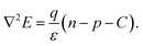 | (12) |
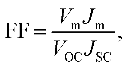
Here, Jn and Jp are the current densities of the electron and hole, respectively. n and p present the density of electrons and holes per unit volume, respectively. μi and Di denote the mobility and diffusivity of i, respectively, where i represents the electron (n) and hole (p). The famous Einstein equation relates mobility and diffusivity. Ri, C, and ε are the net recombination, the contribution from the ionized impurity density, and the dielectric constant, respectively. Fill factor (FF), a performance parameter of a solar cell, was calculated by,| |  | (13) |
| |  | (14) |
and| | 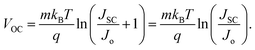 | (15) |
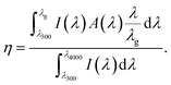
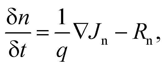
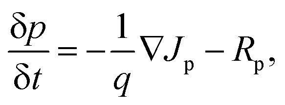
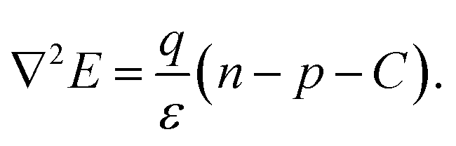
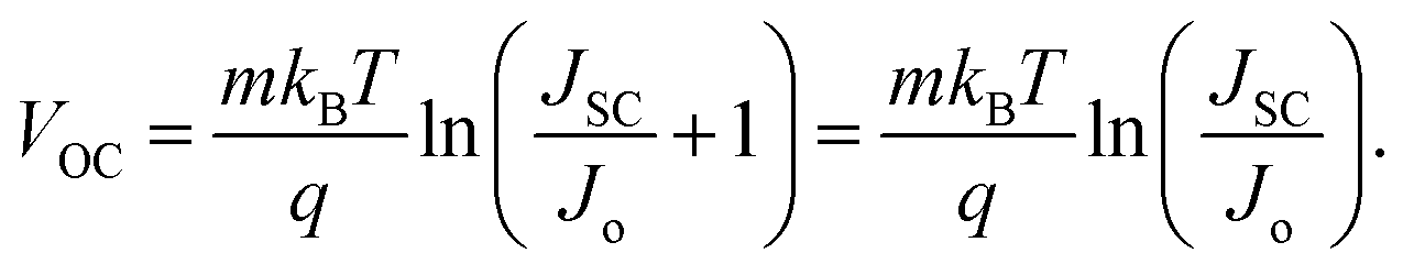
Here, Vm and Jm are the maximum achievable voltage and current density from the cell, and the maximum power, Pm, is shown in the dotted portion of Fig. 7(a). m and Jdark represent the ideality factor and the dark saturation current, respectively. A and T are the surface area and the temperature, respectively. The Pm was calculated to be 31.7 mW cm−2 with an FF of 80.42%. The solar performances of structures I–IV are enlisted in Table S3 of the ESI.† The energy band diagram of the double-grating metamaterial absorber under solar illumination is presented in Fig. 7(b). Two depletion regions were formed between the AlGaAs–Ge and Ge–GaAs interfaces. As the thickness of the Ge layer was thin, the Ge layer acted as a carrier accelerator because the built-in electric field of the depletion region in the Ge layer was very strong and swept carriers from the Ge layer. When photons were incident on the structure, electron–hole pairs were generated. Electrons flowed to the GaAs layer and were collected by the Ti layer. On the other hand, holes flowed through the p-type AlGaAs layer and were collected in a lateral metal contact. JSC from absorbed light and Jdark from light emission both contributed to the total current density of the solar cell, J. Notably, the increase of JSC and reduction of Jdark are desirable for designing an ideal-like solar cell. As J is the sum of JSC and Jdark from eqn (7), we can illustrate an equivalent circuit diagram of our proposed solar cell in Fig. 7(c). Eqn (14) is only applicable for Rs = 0 Ω and Rsh = ∞ Ω. The term 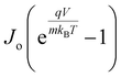 was replaced with
  in eqn (14) while we calculated J–V for various Rs and Rsh conditions. Fig. 7(d) and (e) exhibit the effects of varying Rs and Rsh on the J–V characteristics. Rs arose from the resistance of the cell materials to the current flow in the devices, and Rsh arose from the leakage of current through the devices. Specifically, Rs and Rsh originated on the surfaces and edges of the device, respectively. Low Rs and high Rsh are required for designing an ideal-like solar cell. Our proposed structure exhibited maximum efficiency when Rs = 0 Ω and Rsh = ∞ Ω were utilized. Moreover, the impact of doping concentrations and solar performance analysis are given in Table S4 and Fig. S7 of the ESI.†
 |
| | Fig. 7 (a) J–V (blue curve) and P–V (red curve) characteristics of the proposed double-grating metamaterial structure under unpolarized light. The table shows the performance of the metamaterial double-grating structure. (b) Energy band diagram for our proposed structure IV under solar illumination. (c) Illustration of equivalent circuitry of a solar cell. JSC and Jdark contribute to the total current density of the solar cell, J. J–V characteristics of the proposed double-grating metamaterial absorber varying (d) series resistance, Rs and (e) shunt resistance, Rsh under unpolarized light. (f) Theoretically calculated ultimate efficiency, η of structures I–IV. | |
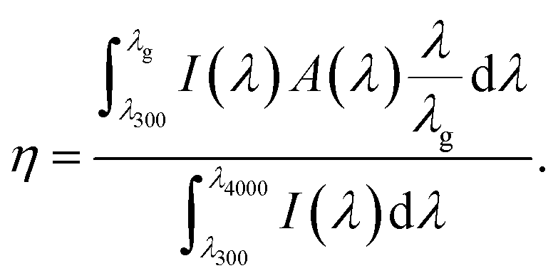
Ultimate efficiency (η), a theoretical performance parameter of the solar cell, was calculated from the absorption spectrum. The η is given by,46
| |  | (16) |
Here, the lower limit (
λ = 300 nm) and upper limit (
λ = 4000 nm) in the denominator represent the limit of data available for the solar spectrum. We enumerated the
η of ∼44% for our proposed structure IV under unpolarized incident light without contact effects and doping, as depicted in
Fig. 7(f). While contact effects and doping were introduced, the PCE of 31.7% was obtained by calculating
Pm/
Pin where
Pin is the input power density of the solar spectrum. We obtained a high PCE, overcoming the SQ limit by utilizing different materials of different band gaps in various layers of the metamaterial structure. There have been numerous reports of overcoming the SQ limit using different band gap materials.
35 Increasing
Rs and decreasing
Rsh drastically reduced the FF and PCE of the proposed structure along with efficiency, as can be seen in
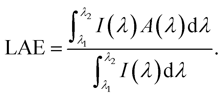
Fig. 7(d) and (e). The LAE, which reveals how much incident light was absorbed by the structure, was calculated. The LAE is given by,
| |  | (17) |
Here,
λ1 and
λ2 represent the calculated LAE range, as shown in
Table 1. We obtained a high LAE of 88.8% under unpolarized light for structure IV in the 450–1000 nm wavelength range. Moreover, a comparatively high LAE for the metamaterial absorber can be found in the wavelength range of 450–3000 nm. A comparative analysis of performance parameters under unpolarized and TM incident light for structures I–IV is enlisted in
Tables 1 and S5 of the ESI,
† respectively.
Table 1 Comparison of theoretical limits of maximum JSC and LAE of structures I–IV under unpolarized light
| Structure |
J
SCmax (mA cm−2) |
LAE (%) |
| 300–λg nm |
450–1000 nm |
450–3000 nm |
| Structure I |
42.1 |
86.2 |
85.2 |
| Structure II |
69.4 |
85.3 |
82.8 |
| Structure III |
48.4 |
86.4 |
85.0 |
| Structure IV |
67.0 |
88.8 |
85.8 |
3.5 Thermal stability under steady state and transient conditions
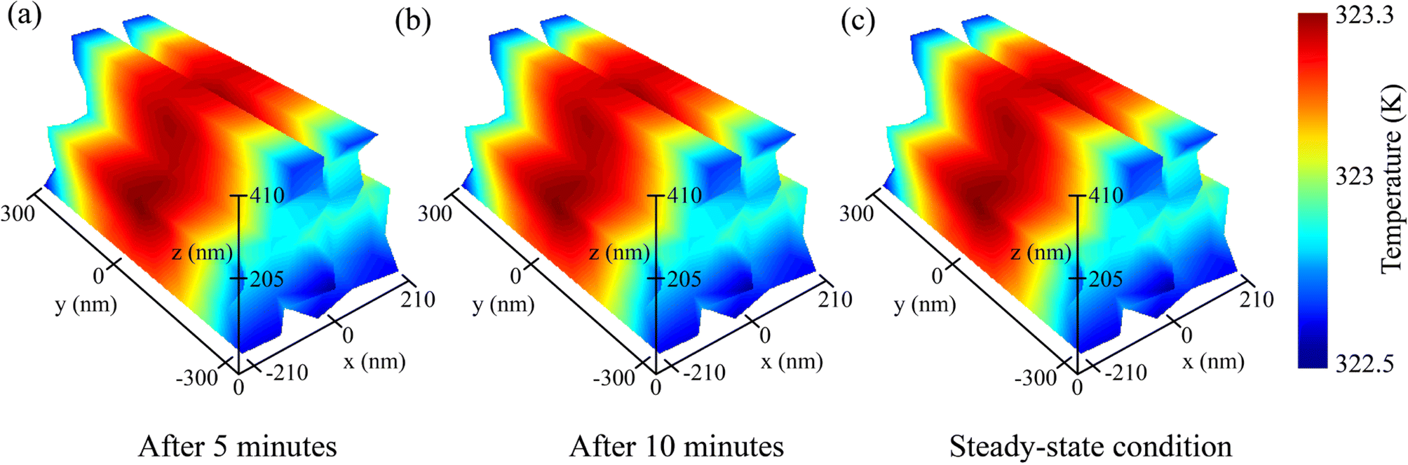
The temperature was increased by ∼23° due to optical absorption from the ambient temperature of 300 K. This elevated temperature decreased the open circuit voltage due to elevated recombination rates. The transient heat temperatures after 5 and 10 minutes are shown in Fig. 8(a) and (b). Fig. 8(c) depicts the steady-state heat temperature of the proposed double-grating metamaterial absorber. Though heat temperature degraded the structure's performance, our proposed double-grating metamaterial structure exhibited thermal stability with time. For better comprehension of the thermal stability, we analyzed the heat temperature profile under different ambient temperature conditions because the solar cells do not only work at 300 K. Therefore, we varied the ambient temperature from 280 to 320 K with an interval of 10 K. We obtained ∼23 K of temperature deviation from its surrounding temperature for all cases (see Fig. S8 of the ESI†). The thermal stability obtained due to the absorption of our proposed structure was independent of temperature.
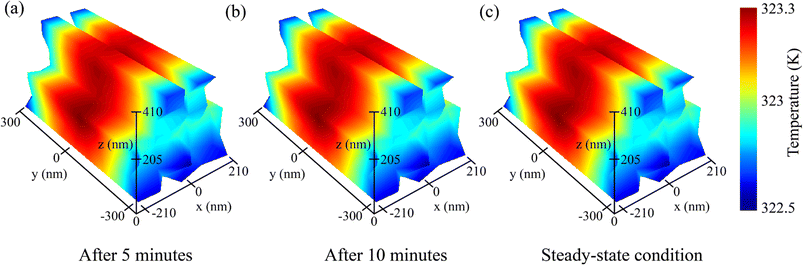 |
| | Fig. 8 Evolution of heat temperature profiles of the proposed metamaterial double-grating structure under transient response after (a) 5 minutes and (b) 10 minutes. (c) Evolution of heat temperature profiles of the proposed metamaterial double-grating structure under steady-state conditions. | |
4 Comparative analysis
Table 2 demonstrates the comparison of performance parameters of our proposed ultra-broadband absorber with those of previously reported absorber studies. Wen et al. reported a GaAs nanowire-based solar cell structure with average absorption greater than 90% in the visible wavelength range.47 The ultrathin Ti–SiO2 cubes32 and multiple cubes absorber44 operated in almost similar wavelength ranges with an average absorption of 97% and 95.1%, respectively. These two had an equal incidence angle tolerability of 60°. The sandwich amorphous silicon43 and TiN metasurface42 structures had an average absorption of greater than 90% operating in the visible and near-infrared regimes, respectively. The GaAs grating array structure proposed by Li et al. had the best short-circuit current density of 56.5 mA cm−2 among the reported studies, with an average absorption of 97%.14 The MIM structure proposed by Qiao et al. had the highest average absorption; however, the operating wavelength bandwidth was limited to 1050 nm.48 In recent times, many research studies have exhibited high absorption at a resonant wavelength.49,50 However, these narrowband efficient absorbers can be minimally used in solar cell applications because the wavelength spectrum of solar irradiance is wide. On the other hand, our proposed double-grating array structure had an average absorption of 98.2% and 96.5% for an ultra-wide wavelength range of 450–2000 nm and 450–3000 nm, respectively, for TM polarized light. Moreover, the theoretical limit of short-circuit current density was significantly higher compared to that in previously reported studies.14,43,47 An extraordinary incidence angle tolerability of 65° was obtained for our proposed double-grating structure. Most importantly, most of the absorbers operated under polarized incident light; however, sunlight has the unpolarized optical properties of light. On the other hand, our proposed structure efficiently absorbed light under both unpolarized and polarized light conditions.
Table 2 Comparative performance analysis of absorbers
| Structure |
Wavelength (nm) |
A
avg (%) |
J
SCmax (mA cm−2) |
δ
|
Incident light |
Ref. |
| GaAs nanowire |
300–700 |
>90 |
28.7 |
— |
Unpolarized |
47
|
| Ti–SiO2–Ti absorber |
350–1400 |
98.21 |
— |
50° |
TM polarized |
48
|
| GaAs grating array |
506–1814 |
97 |
56.5 |
55° |
TM polarized |
14
|
| Sandwich amorphous silicon |
400–700 |
92 |
17.2 |
60° |
TM polarized |
43
|
| TiN metasurface |
316–1426 |
>90 |
— |
45° |
TM polarized |
42
|
| Ultrathin Ti–SiO2 cubes |
354–1066 |
97 |
— |
60° |
TE polarized |
32
|
| Multiple cubes absorber |
405–1505 |
95.1 |
— |
60° |
TE polarized |
44
|
| Double-grating array |
450–2000 |
98.2 |
81.5 |
65° |
TM polarized |
This work |
| 450–3000 |
96.5 |
81.5 |
65° |
TM polarized |
| 450–2000 |
82.2 |
67.0 |
75° |
Unpolarized |
| 450–3000 |
87.0 |
67.0 |
75° |
Unpolarized |
5 Suggested fabrication technique
The fabrication process must be carefully considered for the practical realization of a double-grating ultrathin metamaterial absorber. There are several ways to fabricate our proposed double-grating structure. Silvestre et al. grew a thin GaAs layer onto a Ti slab using the sputtering process.51 However, the accuracy of the crystalline structure is difficult to achieve. Thin film growth techniques, such as metal–organic chemical vapor deposition (MOCVD), chemical vapor deposition (CVD), and molecular beam epitaxy (MBE), can be utilized to obtain better quality crystalline growth and less lattice mismatch. After depositing GaAs onto a Ti slab, the lithography process can be used for patterning and obtaining the double-grating structure. Kim et al. adopted the lithography process to design a GaAs–AlGaAs multilayer grating structure.52Fig. 9 shows a simplified diagram of the suggested fabrication steps that could be taken to build the proposed metamaterial structure. The GaAs layer can be deposited using the MOCVD technique to cover one side of Ti.53 Instead of MOCVD, dynamic hydride vapor phase epitaxy (D-HVPE) can be used because the growth rate is much faster and can exceed 300 μm h−1.54 The lithography process can be used for patterning grating on the GaAs epitaxial layer. Polymethyl methacrylate (PMMA) is generally used as a photoresist because of its excellent film characteristics, ease of handling, and high resolution. Afterward, the Ge layer can be grown on the GaAs layer using the CVD process.55 Moreover, Ge can be grown on GaAs with a tolerable lattice mismatch of around 0.07% using the MBE technique.56 A similar technique can be used to grow AlGaAs bars. More recent work on solute–solvent separation soft lithography can also be conducive to growing AlGaAs layers in our structure.38 A polydimethylsiloxane (PDMS) stamp was used and pressurized for several minutes onto the photoresist to cut out for AlGaAs deposition. The lattice mismatch between the layers is very small, resulting in minimal interface defects.
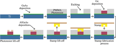 |
| | Fig. 9 Suggested fabrication process of the proposed double-grating metamaterial structure using the solute–solvent separation soft photolithography technique. | |
6 Conclusion
In this study, we numerically analyzed an innovative ultrathin (∼400 nm) metamaterial-based near-perfect broadband solar absorber with an excellent short-circuit current and efficiency. Our proposed structure has the ability to surpass the SQ limit and the tunneling junction impact in tandem solar cells. We utilized GaAs to boost the light absorption and a Ti back reflector to further enhance the absorption process in the AlGaAs/Ge/GaAs absorber layer. To achieve the best possible outcome, we optimized the structure by varying the width, thickness, periodicity, and materials of different layers of the structure. We obtained a high average absorption of 98.2% and 82.2% under TM- and un-polarized light with a peak absorption of 99.9% and 99.7% at 610 and 725 nm for a wavelength range of 450–2000 nm, respectively. The structure exhibited higher polarization independence with incidence angle tolerability up to 75° compared to previously reported studies, which would be versatile for practical use. Solving heat transfer equations reveals that the absorber maintains constant absorption capabilities irrespective of time. The J–V characteristics revealed excellent PCE with a maximum value of 31.7%, where the FF was 80.42%. We obtained an excellent JSC of 47.1 mA cm−2 with a VOC of 0.837 V for our proposed absorber under AM 15 G solar illumination. Our proposed ultrathin double-grating metamaterial absorber not only inspires utilization of the grating structure design for various applications but also has great potential for mitigating the energy crisis by increasing the efficiency of solar cells.
Author contributions
P. P. N. and D. S. conducted the investigation, performed the analysis, wrote the main manuscript text, and prepared the figures. D. S. and P. P. N. contributed equally to this work. M. I. T. helped conduct the study and wrote the main manuscript text. A. Z. supervised and administered the work and wrote the main manuscript text. All authors reviewed the manuscript.
Conflicts of interest
The authors declare no conflict of interest.
Acknowledgements
P. P. Nakti and M. I. Tahmid express gratitude to the Electrical and Electronic Engineering (EEE) department at the Shahjalal University of Science and Technology (SUST) for making available the resources needed to finish their work. D. Sarker acknowledges financial support from the Bangladesh University of Engineering and Technology (BUET) through its Postgraduate Fellowship Program. D. Sarker and A. Zubair thank the EEE department at BUET for providing assistance and resources to complete the work. A. Zubair acknowledges the Basic Research Grant (Sonstha/R-60/Ref-4747) providing by Bangladesh University of Engineering and Technology.
Notes and references
- S. Luo, J. Zhao, D. Zuo and X. Wang, Opt. Express, 2016, 24, 9288–9294 CrossRef CAS PubMed.
- Y. Chen, J. Dai, M. Yan and M. Qiu, Opt. Express, 2013, 21, 20873–20879 CrossRef PubMed.
- M. Mesch, B. Metzger, M. Hentschel and H. Giessen, Nano Lett., 2016, 16, 3155–3159 CrossRef CAS PubMed.
- X. Lu, L. Zhang and T. Zhang, Opt. Express, 2015, 23, 20715–20720 CrossRef CAS PubMed.
- Y. Cheng and J. Zhao, Phys. Scr., 2022, 97, 095508 CrossRef.
- Y. Cheng, F. Chen and H. Luo, Nanoscale Res. Lett., 2021, 16, 12 CrossRef CAS PubMed.
- A. Vora, J. Gwamuri, N. Pala, A. Kulkarni, J. M. Pearce and D. Ö. Güney, Sci. Rep., 2014, 4, 4901 CrossRef CAS PubMed.
- K. Aydin, V. E. Ferry, R. M. Briggs and H. A. Atwater, Nat. Commun., 2011, 2, 517 CrossRef PubMed.
- M. D. Goldflam, E. A. Kadlec, B. V. Olson, J. F. Klem, S. D. Hawkins, S. Parameswaran, W. T. Coon, G. A. Keeler, T. R. Fortune, A. Tauke-Pedretti, J. R. Wendt, E. A. Shaner, P. S. Davids, J. K. Kim and D. W. Peters, Appl. Phys. Lett., 2016, 109, 251103 CrossRef.
- C. Argyropoulos, K. Q. Le, N. Mattiucci, G. D'Aguanno and A. Alù, Phys. Rev. B: Condens. Matter Mater. Phys., 2013, 87, 205112 CrossRef.
- Y. Gong, Z. Wang, K. Li, L. Uggalla, J. Huang, N. Copner, Y. Zhou, D. Qiao and J. Zhu, Opt. Lett., 2017, 42, 4537–4540 CrossRef CAS PubMed.
- S. Vanka, B. Zhou, R. A. Awni, Z. Song, F. A. Chowdhury, X. Liu, H. Hajibabaei, W. Shi, Y. Xiao, I. A. Navid, A. Pandey, R. Chen, G. A. Botton, T. W. Hamann, D. Wang, Y. Yan and Z. Mi, ACS Energy Lett., 2020, 5, 3741–3751 CrossRef CAS.
- M. Chirumamilla, A. Chirumamilla, Y. Yang, A. S. Roberts, P. K. Kristensen, K. Chaudhuri, A. Boltasseva, D. S. Sutherland, S. I. Bozhevolnyi and K. Pedersen, Adv. Opt. Mater., 2017, 5, 1700552 CrossRef.
- Y. Li, Q. Chen, B. Wu, L. Shi, P. Tang, G. Du and G. Liu, Results Phys., 2019, 15, 102760 CrossRef.
- M. I. Tahmid, M. A. Z. Mamun and A. Zubair, Opt. Mater. Express, 2021, 11, 1267–1281 CrossRef.
- U. K. Kumawat, K. Kumar, S. Mishra and A. Dhawan, J. Opt. Soc. Am. B, 2020, 37, 495–504 CrossRef CAS.
- M. Shimizu, Z. Liu and H. Yugami, ACS Appl. Nano Mater., 2020, 3, 9502–9509 CrossRef CAS.
- V. G. Veselago, Phys.-Usp., 1968, 10, 509 CrossRef.
- A. Alu and N. Engheta, IEEE Trans. Antennas Propag., 2007, 55, 3027–3039 Search PubMed.
- Y. Ye, Y. Zhang, Y. Zhao, Y. Ren and X. Ren, Opt. Express, 2021, 29, 15255–15268 CrossRef CAS PubMed.
- W. Cai, U. K. Chettiar, A. V. Kildishev and V. M. Shalaev, Nat. Photonics, 2007, 1, 224–227 CrossRef CAS.
- D. R. Smith, J. B. Pendry and M. C. K. Wiltshire, Science, 2004, 305, 788–792 CrossRef CAS PubMed.
- D. Sarker, P. P. Nakti, M. I. Tahmid, M. A. Z. Mamun and A. Zubair, Opt. Express, 2021, 29, 42713–42725 CrossRef CAS.
- D. Sarker, P. P. Nakti, M. I. Tahmid, M. A. Z. Mamun and A. Zubair, Opt. Quantum Electron., 2023, 55, 159 CrossRef CAS.
- N. Akhtary and A. Zubair, Opt. Mater. Express, 2023, 13, 2759–2774 CrossRef.
- A. Mukherjee, D. Ren, P.-E. Vullum, J. Huh, B.-O. Fimland and H. Weman, ACS Photonics, 2021, 8, 2355–2366 CrossRef CAS.
- B. Wang, C. Ma, P. Yu, A. O. Govorov, H. Xu, W. Wang, L. V. Besteiro, Z. Jing, P. Li and Z. Wang, Photonics Res., 2022, 10, 2718–2727 CrossRef.
- G. Cheek and R. Mertens, Sol. Cells, 1983, 8, 17–32 CrossRef CAS.
-
J. Nelson, The Physics of Solar Cells, Imperial College Press, 2003 Search PubMed.
- M. Luo, S. Shen, L. Zhou, S. Wu, Y. Zhou and L. Chen, Opt. Express, 2017, 25, 16715–16724 CrossRef CAS PubMed.
- Y. Wang, K. Chen, Y.-S. Lin and B.-R. Yang, Phys. E, 2022, 139, 115140 CrossRef.
- L. Lei, S. Li, H. Huang, K. Tao and P. Xu, Opt. Express, 2018, 26, 5686–5693 CrossRef CAS PubMed.
- B.-X. Wang, C. Tang, Q. Niu, Y. He and R. Chen, Nanoscale Adv., 2019, 1, 3621–3625 RSC.
- X. Cheng, R. Huang, J. Xu and X. Xu, ACS Appl. Mater. Interfaces, 2020, 12, 33352–33360 CrossRef CAS PubMed.
- Z. Yu, S. Sandhu and S. Fan, Nano Lett., 2014, 14, 66–70 CrossRef CAS PubMed.
- J. Hwang, B. Oh, Y. Kim, S. Silva, J. O. Kim, D. A. Czaplewski, J. E. Ryu, E. K. Kim, A. Urbas, J. Zhou, Z. Ku and S. J. Lee, Sci. Rep., 2018, 8, 14787 CrossRef PubMed.
- H. Guo, J. Tang, K. Qian, D. Tsoukalas, M. Zhao, J. Yang, B. Zhang, X. Chou, J. Liu, C. Xue and W. Zhang, Sci. Rep., 2016, 6, 23606 CrossRef CAS PubMed.
- X. Dai and H. Xie, Opt. Mater. Express, 2016, 6, 1530–1544 CrossRef CAS.
-
E. D. Palik, Handbook of Optical Constants of Solids, Academic Press, Boston, 1998, p. iii Search PubMed.
- S. Adachi, J. Appl. Phys., 1989, 66, 6030–6040 CrossRef CAS.
- M. Burgelman, P. Nollet and S. Degrave, Thin Solid Films, 2000, 361–362, 527–532 CrossRef CAS.
- Z. Liu, G. Liu, Z. Huang, X. Liu and G. Fu, Sol. Energy Mater. Sol. Cells, 2018, 179, 346–352 CrossRef CAS.
- S. Wu, Y. Ye, M. Luo and L. Chen, J. Opt. Soc. Am. B, 2018, 35, 1825–1828 CrossRef CAS.
- J. Liu, W.-Z. Ma, W. Chen, G.-X. Yu, Y.-S. Chen, X.-C. Deng and C.-F. Yang, Opt. Express, 2020, 28, 23748–23760 CrossRef CAS PubMed.
- J. Tauc, Mater. Res. Bull., 1968, 3, 37–46 CrossRef CAS.
- N. Huang, C. Lin and M. L. Povinelli, J. Opt., 2012, 14, 024004 CrossRef.
- L. Wen, Z. Zhao, X. Li, Y. Shen, H. Guo and Y. Wang, Appl. Phys. Lett., 2011, 99, 143116 CrossRef.
-
Y.-j. Qiao, X.-h. Lu, W.-b. Li, Y.-r. Su, L. Li, Z.-w. Xie and M.-j. Tang, International Conference on Optoelectronic and Microelectronic Technology and Application, 2020, pp. 228–234 Search PubMed.
- H. Zhang, Y. Cheng and F. Chen, Optik, 2021, 229, 166300 CrossRef CAS.
- Z. Li, Y. Cheng, H. Luo, F. Chen and X. Li, J. Alloys Compd., 2022, 925, 166617 CrossRef CAS.
-
S. Silvestre, J. Puigdollers, A. Boronat and L. Castaner, 2009Spanish Conference on Electron Devices, 2009, pp. 5–7 Search PubMed.
- H. Kim, S.-Y. Ahn and Z. Wasilewski, J. Vac. Sci. Technol., B: Nanotechnol. Microelectron.: Mater., Process., Meas., Phenom., 2019, 37, 031209 Search PubMed.
- K. J. Schmieder, E. A. Armour, M. P. Lumb, M. K. Yakes, Z. Pulwin, J. Frantz and R. J. Walters, IEEE J. Photovolt., 2017, 7, 340–346 Search PubMed.
- W. Metaferia, K. L. Schulte, J. Simon, S. Johnston and A. J. Ptak, Nat. Commun., 2019, 10, 3361 CrossRef PubMed.
- T. F. Kuech, M. Mäenpää and S. S. Lau, Appl. Phys. Lett., 1981, 39, 245–247 CrossRef CAS.
- G. Dushaq and M. Rasras, Sci. Rep., 2019, 9, 14221 CrossRef PubMed.
Footnotes |
| † Electronic supplementary information (ESI) available: Multimedia files for supporting content. See DOI: https://doi.org/10.1039/d3na00565h |
| ‡ These authors contributed equally to this work. |
|
| This journal is © The Royal Society of Chemistry 2023 |
Click here to see how this site uses Cookies. View our privacy policy here. 
 Open Access Article
 This Open Access Article is licensed under a Creative Commons Attribution-Non Commercial 3.0 Unported Licence
 a,
Dip
Sarker‡
a,
Dip
Sarker‡


 was replaced with
 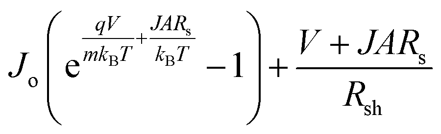 in eqn (14) while we calculated J–V for various Rs and Rsh conditions. Fig. 7(d) and (e) exhibit the effects of varying Rs and Rsh on the J–V characteristics. Rs arose from the resistance of the cell materials to the current flow in the devices, and Rsh arose from the leakage of current through the devices. Specifically, Rs and Rsh originated on the surfaces and edges of the device, respectively. Low Rs and high Rsh are required for designing an ideal-like solar cell. Our proposed structure exhibited maximum efficiency when Rs = 0 Ω and Rsh = ∞ Ω were utilized. Moreover, the impact of doping concentrations and solar performance analysis are given in Table S4 and Fig. S7 of the ESI.†