
 Open Access Article
 This Open Access Article is licensed under a Creative Commons Attribution-Non Commercial 3.0 Unported Licence
A mixed-dimensional quasi-1D BiSeI nanowire-2D GaSe nanosheet p–n heterojunction for fast response optoelectronic devices†
Huijie
Hu
ab,
Weili
Zhen
a,
Zhilai
Yue
a,
Rui
Niu
a,
Feng
Xu
a,
Wanli
Zhu
a,
Keke
Jiao
a,
Mingsheng
Long
 c,
Chuanying
Xi
*a,
Wenka
Zhu
*a and
Changjin
Zhang
*acd
c,
Chuanying
Xi
*a,
Wenka
Zhu
*a and
Changjin
Zhang
*acd
aHigh Magnetic Field Laboratory of Anhui Province, HFIPS, Chinese Academy of Sciences, Hefei 230031, China. E-mail: xcy@hmfl.ac.cn; wkzhu@hmfl.ac.cn; zcjin@ustc.edu.cn
bScience Island Branch of Graduate School, University of Science and Technology of China, Hefei 230026, China
cInformation Materials and Intelligent Sensing Laboratory of Anhui Province, Institutes of Physical Science and Information Technology, Anhui University, Hefei 230601, China
dCollaborative Innovation Center of Advanced Microstructures, Nanjing University, Nanjing 210093, China
First published on 6th October 2023
Abstract
Due to the unique combination configuration and the formation of a built-in electric field, mixed-dimensional heterojunctions present fruitful possibilities for improving the optoelectronic performances of low-dimensional optoelectronic devices. However, the response times of most photodetectors built from mixed-dimensional heterojunctions are within the millisecond range, limiting their applications in fast response optoelectronic devices. Herein, a mixed-dimensional BiSeI/GaSe van der Waals heterostructure is designed, which exhibits visible light detection ability and competitive photoresponsivity of 750 A W−1 and specific detectivity of 2.25 × 10¹² Jones under 520 nm laser excitation. Excitingly, the device displays a very fast response time, e.g., the rise time and decay time under 520 nm laser excitation are 65 μs and 190 μs, respectively. Our findings provide a prospective approach to mixed-dimensional heterojunction photodetection devices with rapid switching capabilities.
Introduction
The discovery of graphene in 2004 opened a new research field of two-dimensional (2D) materials, which not only exhibit many intriguing new phenomena in fundamental science but also possess vast potential for industrial applications across diverse disciplines.1–6 Among the huge application aspects of 2D materials, the photodetectors built from 2D materials generally exhibit high photoresponsivity, broadband spectrum detection, and fast response compared to those built from conventional three-dimensional thin films.7 In recent years, various types of photodetectors built from different 2D materials have been designed, including graphene, black phosphorus, hexagonal boron nitride, transition metal dichalcogenides, and highly stable oxide perovskites, as well as many ternary sulfide compounds.8–16 Benefiting from the excellent mechanical properties of 2D materials, the flexible 2D materials can be easily integrated with other 2D materials by versatile facile exfoliation and transfer strategies, leading to various types of van der Waals (vdW) heterojunctions. The ability to engineer the band structures and excitonic states of 2D materials in vdW heterojunctions greatly enhances the optoelectronic performances of photodetectors. Based on this fact, various types of vdW heterojunctions, such as the perovskite junction with tunable work function MXene electrodes, MXene/GaN, MoSe2/GaSe, MoS2/WSe2, GaSe/InSe, and black phosphorus/MoS2, have been constructed in order to achieve high performances of optoelectronic devices.17–24Meanwhile, due to the nature of dangling bond-free surfaces, 2D materials could also be integrated with different dimensional materials such as 0D quantum dots, 1D nanowires, and 3D materials, leading to the so-called mixed-dimensional vdW heterostructures without consideration of lattice mismatch.25 Different mixed-dimensional heterostructures, such as 1D p-CuO/2D n-MoS2,26 1D p-Te/2D n-ReS2,27 and 2D MoS2/3D Ge,28 have been built. Rapid photoresponse,29 ultrahigh photoresponsivity,30 and broadband photoresponse31 have been demonstrated in mixed-dimensional integration systems. Though the optoelectronic performances have been significantly enhanced in these mixed-dimensional heterojunctions, the response time of mixed-dimensional heterostructures is mostly within the millisecond range, limiting their application prospects in rapid switching photodetection devices.29–31
Gallium selenide (GaSe) is a p-type semiconductor which exhibits a direct bandgap of about 2 eV.32 In recent years, GaSe has aroused significant research attention as a potential material platform for building high-performance photodetectors.33–36 An ultrathin GaSe-based photodetector exhibits a high photoresponsivity of 2.8 A W−1 and high external quantum efficiency of 1367% at 254 nm.33 Though the response time of a GaSe-based photodetector could be as fast as 0.02 s, it is still within the millisecond range. As a matter of fact, the response times of photodetectors based on GaSe heterojunction are mostly in the range of seconds to milliseconds.33–36 Thus, an efficient strategy to shorten the response time of a GaSe-based photodetector is of great importance in extending the application fields of such low-dimensional materials.
In this work, we construct a mixed-dimensional quasi-1D BiSeI nanowire-2D GaSe nanosheet p–n heterojunction photodetector. The photodetector exhibits a very high photoresponsivity of 750 A W−1 and a specific detectivity of 2.25 × 10¹² Jones at 520 nm. Importantly, we find that the rise and decay times of the mixed-dimensional heterojunction device could be as fast as 65 μs and 190 μs, respectively. The present results demonstrate that the mixed-dimensional BiSeI/GaSe heterostructure is of great potential in building photodetectors with both high responsivity and fast response.
Results and discussion
The characterization of BiSeI and GaSe single crystals confirms that BiSeI is a n-type semiconductor with a narrow bandgap of about 1.1 eV and GaSe is a p-type semiconductor with a bandgap of about 2 eV. The detailed characterization studies of the crystal structures, bandgaps and electrical properties are given in ESI Fig. S1 and S2.† In this work, we dedicate to investigate the optoelectronic performances of a mixed-dimensional heterojunction built from quasi-1D BiSeI nanowires and 2D GaSe nanosheets. Fig. 1(a) shows the 3D diagram of the BiSeI/GaSe heterostructure. For the fabrication of the photodetector, a dry physical transfer method is used to vertically stack the BiSeI nanowire and GaSe nanosheet. Cr/Au electrodes are fabricated through the process of thermal evaporation following ultra-violet maskless lithography. To avoid interference from non-contact regions, we only expose the essential vertical portions of the BiSeI and GaSe heterostructure, as the surface of GaSe is significantly larger than that of the BiSeI nanowire.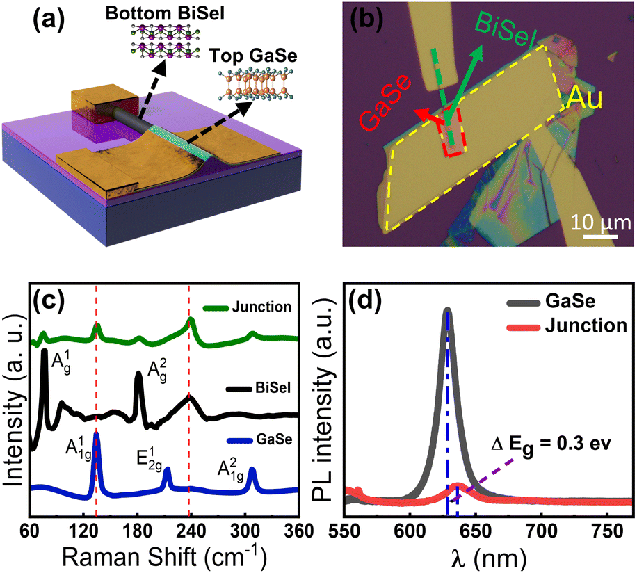 | ||
| Fig. 1 (a) The 3D diagram of the BiSeI/GaSe heterostructure photodetector. (b) Optical microscopy image and (c) Raman spectra of individual BiSeI, GaSe and the BiSeI/GaSe heterojunction under 532 nm laser excitation. (d) Photoluminescence spectra of individual GaSe and the BiSeI/GaSe heterojunction. | ||
Fig. 1(b) shows the optical microscopy image of the heterojunction on the Si/SiO2 substrate with Cr/Au (10 nm/80 nm) electrodes. As shown in Fig. S3,† the thicknesses of the BiSeI nanowire, the GaSe nanosheet, and the heterojunction are determined to be 430 nm, 70 nm, and 500 nm, respectively. To confirm the quality of the heterojunction, Raman spectra under the excitation of a 532 nm laser are measured. Fig. 1(c) exhibits the Raman spectra acquired from the individual BiSeI nanowire and GaSe nanosheet, as well as the heterojunction region. It can be seen that the characteristic Raman peaks of individual BiSeI and GaSe are consistent with previous reports.33,37 The Raman peaks located at 76.5 and 182 cm−1 in the Raman spectra of BiSeI nanowires correspond to the Ag vibration modes. And the peaks appearing at 133, 212, and 307 cm−1 are assigned to the Ag and Eg vibration modes of GaSe.33,37 A slight redshift of the Raman peaks located at 133 and 241 cm−1 could be found, which is due to the electron injection effects in the heterojunction.38,39 Compared to the individual components, the Raman peaks of the overlapped BiSeI/GaSe vdW heterostructure exhibit a noticeable reduction in intensity. The quenching effect in the intensity of Raman peaks signifies the strong interfacial coupling between BiSeI and GaSe, providing evidence for the good contact at the vdW heterojunction.40
The photoluminescence (PL) measurements are performed using a 532 nm laser to examine the contact at the BiSeI/GaSe interface. Fig. 1(d) shows the PL spectra of the BiSeI/GaSe heterostructure and individual GaSe. It should be noted that BiSeI shows no obvious PL signal due to its indirect bandgap. The GaSe nanosheet exhibits a predominant PL peak at 628 nm, consistent with its bandgap of 2 eV. For the BiSeI/GaSe heterojunction, a small shift in the PL peak position could be observed compared to that of individual GaSe, which corresponds to an energy shift of about 0.3 eV. Meanwhile, an obvious quenching effect in the PL spectra could be observed in the BiSeI/GaSe heterojunction. The quenching effect in PL spectra suggests the occurrence of efficient electron separation and transfer at the interface of the heterostructure, providing evidence of strong interlayer coupling at the interface.40
Fig. 2(a) and (c) give the Ids (drain-source current)–Vds (drain-source voltage) curves at Vds = ±2 V for the GaSe nanosheet and the BiSeI nanowire, which indicate good ohmic contacts of the output characteristics. The presence of ohmic contact in the electrical measurements indicates that a good pathway for electron transfer has been set up. In an n-type semiconductor, the application of gate voltage (Vgs) results in an accumulation of electrons, leading to a rise in the drain current (Ids). Conversely, in a p-type semiconductor, a depletion of holes occurs with increasing Vgs, leading to a reduction of Ids. The transfer curves shown in Fig. 2(b) and (d) reveal that the GaSe nanosheet exhibits p-type conductivity, while the BiSeI nanowire demonstrates typical n-type behaviour. The electrical characterization of the BiSeI/GaSe heterojunction under dark conditions is shown in Fig. 2(e). The Ids ∼ Vds curve of the heterojunction exhibits good rectification behaviour with a rectification ratio of approximately 104 at Vds = ±2 V.
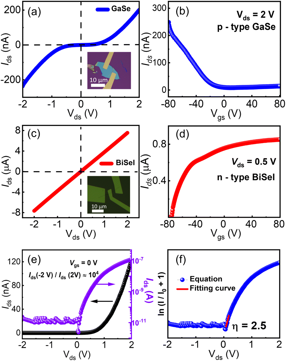 | ||
| Fig. 2 (a and c) The output characteristics of individual GaSe and BiSeI. The insets show the optical images of the GaSe and BiSeI devices. (b and d) The transfer characteristics of the individual GaSe and BiSeI. (e and f) The Ids ∼ Vds of the BiSeI/GaSe heterojunction and fitting curve. | ||
The high rectification ratio indicates the presence of a high-quality interface between the BiSeI nanowire and GaSe nanosheet, which is hardly affected by any impurities or amorphous layers.41 The rectifying I ∼ V curve could be expressed as
 | (1) |
η = q/kT(∂V/(∂ln![[thin space (1/6-em)]](https://www.rsc.org/images/entities/char_2009.gif) I)), I)), | (2) |
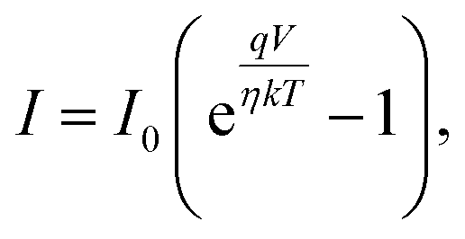
Fig. 3(a) gives the Ids ∼ Vds curves of the BiSeI/GaSe heterostructure under dark conditions and 520 nm laser illumination from 0.2 to 20 mW cm−2. We have given the results for 405 nm, 488 nm and 635 nm laser illumination in Fig. S4.† As shown in Fig. 3(a), an obvious photoresponse is found under forward bias (Vds > 0 V), suggesting the increase in photo-induced carriers. However, the photocurrent is small under reverse bias (Vds < 0 V), indicating that the BiSeI/GaSe heterostructure operates in the off state.
 | ||
| Fig. 3 (a) The output curve of the device under 520 nm laser illumination with five different power densities of 0.2, 2, 4, 12 and 20 mW cm−2. (b) The relationship between power density and illumination current at Vds = 2 V. (c and d) The corresponding R and D* with different power densities at Vds = 2 V under 405 nm, 488 nm, 520 nm and 635 illumination. | ||
We give an energy band diagram of the BiSeI/GaSe heterojunction to explain the photoelectric response processes in Fig. S5.† When BiSeI/GaSe form a junction, their charge carriers go through a diffusion process, which subsequently reaches an equilibrium condition. As a result of this equilibration, the Fermi levels of the BiSeI and GaSe become aligned to reach a dynamic equilibrium and form an internal electric field. When light is applied, the electrons and holes are excited. As the aggregation increases, the built-in electric field is weakened. The potential barrier in the space charge region decreases, resulting in a large photocurrent under a positive conduction. The measured overall Ids increases from 350 nA in the dark state to 910 nA under 20 mW cm−2 when a drain voltage of 2 V is applied. From Fig. 3(b), it can be seen that the illumination current exhibits a dependence on the laser wavelength with optical intensity. And no saturation is observed in the measured range. We perform calculations to determine the photoresponsivity (R) and specific detectivity (D*) of the BiSeI/GaSe heterostructure photodetector. The results are depicted in Fig. 3(c) and (d). The photoresponsivity is defined as
 | (3) |
 | (4) |
The switching capabilities of the BiSeI/GaSe heterostructure photodetector are evaluated by measuring its response speed.
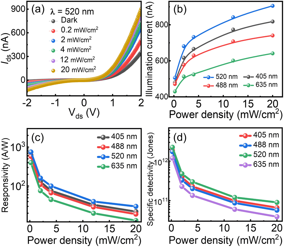
The response speed can be quantified by the rise time (τr) and decay time (τd) of the device. τr represents the duration time of the photocurrent from 10% to 90% of its maximum value, and τd measures the duration of the photocurrent from 90% to 10% of its maximum value.45 Due to the responsivity and specific detectivity of the BiSeI/GaSe heterostructure photodetector exhibiting the best values under 520 nm laser irradiation, A 520 nm laser is selected as the light source to test the response speed with a drain-source voltage of 2 V. In order to have a comparison of the heterojunction device with the individual GaSe and BiSeI photodetector, we give the photoresponse performances of the GaSe and BiSeI photodetectors in Fig. 4 (a–d). It can be seen that the τr and τd values are in the millisecond timescale under 520 nm laser irradiation, except that the τd of the GaSe photodetector is 650 μs. The response performances of the heterostructure device are shown in Fig. 4(e) and (f). It is found that the obtained τr and τd are both in the μs timescale under the same testing conditions. Quantitatively, τr and τd are calculated to be about 65 μs and 190 μs, respectively. The rapid response speed of the heterostructure photodetector suggests efficient separation and transfer of photogenerated charge carriers to different side layers towards the electrodes under the applied bias.40,46
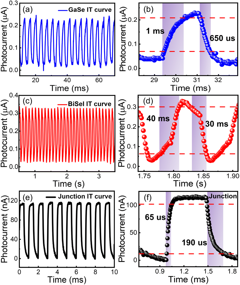 | ||
| Fig. 4 The photoresponse to on/off irradiation showing (a, c, and e) the corresponding photodetector stability of GaSe, BiSeI and the BiSeI/GaSe heterojunction at Vds = 2 V. (b, d, and f) The typical response speed of GaSe, BiSeI and BiSeI/GaSe heterojunction devices. | ||
We conduct a comparison of the photoresponse performance between the present 1D BiSeI nanowire/2D GaSe nanosheet heterojunctions and those of other mixed-dimensional 1D/2D heterojunctions. The summarized results are given in Table 1.42,47–54 The BiSeI/GaSe heterostructure exhibits the fastest response speed among the 1D/2D heterojunction photodetectors in the table. The remarkable performance of the BiSeI/GaSe heterostructure can be attributed to the intrinsic electric field present at the heterostructure interface and the stimulation from laser irradiation. These factors enhance the effective separation and transport of charge carriers, leading to its competitive performance.
| Heterojunction | V ds [V] | Light [nm] | R [A W−1] | D* [Jones] | τ r | τ d | Ref. |
|---|---|---|---|---|---|---|---|
| 1D Te/2D MoTe2 | −1 | 520 nm | 3 × 10⁴ | 4.9 × 10¹¹ | 4.8 ms | 24.6 ms | 47 |
| 1D SbSI/2D PbI2 | 5 | 650 nm | 2.6 × 10⁻² | 4.4 × 10¹³ | 12 ms | 8 ms | 48 |
| 1D Se/2D InSe | 0 | 460 nm | 3.2 × 10⁻² | 1.7 | 30 ms | 37 ms | 49 |
| 1D CdS/2D MoTe2 | 0 | White | 6 × 10⁻² | — | 50 ms | 50 ms | 50 |
| 1D ZnO/2D WSe2 | −5 | 620 nm | 0.23 | — | 50 ms | 50 ms | 42 |
| 1D CuO/2D MoS2 | −2 | 600 nm | 1.6 × 10⁵ | — | 34.6 ms | 51.9 ms | 51 |
| 1D CdS/2D WSe2 | 2 | 680 nm | 3.3 × 10⁴ | — | 1000 ms | 1000 ms | 52 |
| 1D Te/2D Bi2O2Se | 0 | 532 nm | 0.77 | 1.5 × 10⁹ | 400 μs | 402 μs | 53 |
| 1D GaAs/2D perovskite | −3 | 532 nm | 75 | 1.49 × 10¹¹ | 1.2 ms | 0.5 ms | 54 |
| 1D BiSeI/2D GaSe | 2 | 520 nm | 750 | 2.25 × 10¹² | 65 μs | 190 μs | This work |
Conclusions
In summary, a mixed-dimensional 1D BiSeI nanowire/2D GaSe nanosheet heterojunction is designed. The Raman and PL spectra confirm the presence of a strong interlayer coupling between BiSeI and GaSe. As a result, the optoelectronic device built from the BiSeI/GaSe heterojunction shows competitive optoelectronic performances of photoresponsivity of 750 A W−1 and the maximum specific detectivity of 2.25 × 10¹² Jones under 520 nm laser irradiation. Meanwhile, the device exhibits a fast photoelectronic response of τr ∼65 μs and τd ∼190 μs under 520 nm laser irradiation. The present heterojunction extends the application prospect of GaSe in rapid switching photodetection devices.Experimental section
Growth of BiSeI and GaSe single crystals
Single crystals of BiSeI were grown using a two-step method. First, polycrystalline BiSeI was grown using a solid state reaction technique. The BiSeI polycrystalline samples were loaded into a quartz ampoule and sealed under 10−5 Pa. The sealed ampoule was put into a two-temperature-zone furnace. The source zone (T1) of raw materials was gradually heated to 600 °C in 24 h and maintained for 12 h. Then, the furnace was cooled down to 400 °C and kept at this temperature for 24 h for homogenization before cooling down to room temperature. During the growth process, the temperature of the growth zone (T2) was set 15 °C lower than the source zone.Single crystals of GaSe were grown using Ga granules and selenium powder as the starting materials. Iodine granules were used as the transport agent. The raw materials were transferred into a quartz ampoule and sealed. The ampoule was placed into a muffle furnace and heated to 800 °C. The furnace was kept at 800 °C for 12 h and then cooled to room temperature. Single crystals of GaSe with dimensions of 1 × 1 × 0.05 mm3 were obtained at the walls of the ampoule.
Device fabrication
BiSeI nanowires were exfoliated from bulk BiSeI single crystals with the blue film tape and transferred onto the SiO2/Si substrate under an argon atmosphere. The substrate was heated on a hotplate at 100 °C for 3 minutes. Then, GaSe nanosheets were transferred onto one end of the BiSeI nanowires using a two-dimensional transfer platform (Meta test E1-M), leaving the other end of the nanowires exposed. The heterostructures were placed in an argon atmosphere and annealed at 100 °C for 5 minutes. Finally, two Cr/Au (10 nm/80 nm) electrodes were deposited on the end of the BiSeI nanowires and GaSe nanosheets, respectively.Characterization
A PARK NX10 atomic force microscope was used to characterize the morphological structure and thickness of the samples. A LabRam HR800 confocal Raman spectrometer was used to characterize the structural properties of the samples. UV-visible-infrared spectrophotometry (UV3600-MPC3100) and photoluminescence spectroscopy (HORIBA LabRam HR) were used to characterize the electronic structures of BiSeI and GaSe samples. The electrical and photoelectric properties of the heterojunction were measured using a program-controlled semiconductor characterization system (Keithley 2636B) and a probe station.Author contributions
The single crystals of BiSeI and GaSe were grown by Huijie Hu, Wanli Zhu, and Keke Jiao. The characterization studies of the crystal structure and bandgaps were performed by Huijie Hu and Feng Xu. The BiSeI/GaSe heterojunctions were constructed by Huijie Hu, Weili Zhen, and Zhilai Yue. The optoelectronic performances of the individual BiSeI, GaSe and the BiSeI/GaSe heterojunctions were measured and analyzed by Huijie Hu, Weili Zhen, Mingsheng Long, Chuanying Xi, and Changjin Zhang. Huijie Hu, Wenka Zhu, and Changjin Zhang wrote the manuscript. Chuanying Xi, Wenka Zhu, and Changjin Zhang coordinated the whole work. All authors had given approval to the final version of the manuscript.Conflicts of interest
There are no conflicts to declare.Acknowledgements
This work was supported by the National Key R&D Program of China (Grant No. 2021YFA1600201 and 2022YFA1403203), the National Natural Science Foundation of China (Grant No. 11974356, and 12274414), and the Joint Funds of the National Natural Science Foundation of China and the Chinese Academy of Sciences Large-Scale Scientific Facility under Grant No. U1932216.References
- K. S. Novoselov, A. K. Geim, S. V. Morozov, D. Jiang, Y. Zhang, S. V. Dubonos, I. V. Grigorieva and A. A. Firsov, Science, 2004, 306, 666–669 CrossRef CAS PubMed.
- B. Radisavljevic, A. Radenovic, J. Brivio, V. Giacometti and A. Kis, Nat. Nanotechnol., 2011, 6, 147–150 CrossRef CAS PubMed.
- K. H. Lee, H. J. Shin, J. Lee, I. Y. Lee, G. H. Kim, J. Y. Choi and S. W. Kim, Nano Lett., 2012, 12, 714–718 CrossRef CAS PubMed.
- M. Huang, M. Wang, C. Chen, Z. Ma, X. Li, J. Han and Y. Wu, Adv. Mater., 2016, 28, 3481–3485 CrossRef CAS PubMed.
- M. Peng, R. Xie, Z. Wang, P. Wang, F. Wang, H. Ge, Y. Wang, F. Zhong, P. Wu, J. Ye, Q. Li, L. Zhang, X. Ge, Y. Ye, Y. Lei, W. Jiang, Z. Hu, F. Wu, X. Zhou, J. Miao, J. Wang, H. Yan, C. Shan, J. Dai, C. Chen, X. Chen, W. Lu and W. Hu, Sci. Adv., 2021, 7, eabf7358 CrossRef CAS PubMed.
- Y. Chen, Y. Wang, Z. Wang, Y. Gu, Y. Ye, X. Chai, J. Ye, Y. Chen, R. Xie, Y. Zhou, Z. Hu, Q. Li, L. Zhang, F. Wang, P. Wang, J. Miao, J. Wang, X. Chen, W. Lu, P. Zhou and W. Hu, Nat. Electron., 2021, 4, 357–363 CrossRef CAS.
- C. H. Liao, M. A. Mahmud and A. W. Y. Ho-Baillie, Nanoscale, 2023, 15, 4219–4235 RSC.
- R.-J. Shiue, Y. Gao, Y. Wang, C. Peng, A. D. Robertson, D. K. Efetov, S. Assefa, F. H. L. Koppens, J. Hone and D. Englund, Nano Lett., 2015, 15, 7288–7293 CrossRef CAS PubMed.
- B. Tan, H. Yang, Y. Hu, F. Gao, L. Wang, M. Dai, S. Zhang, H. Shang, H. Chen and P. Hu, ACS Appl. Mater. Interfaces, 2020, 12, 28351–28359 CrossRef CAS PubMed.
- H. Zhao, Y. Yan, X. Song, Z. Ma, T. Tian, Y. Jiang, X. Li, C. Xia and J. Li, Nanoscale, 2021, 13, 3757–3766 RSC.
- Y. Zou, Z. Zhang, J. Yan, L. Lin, G. Huang, Y. Tan, Z. You and P. Li, Nat. Commun., 2022, 13, 4372 CrossRef CAS PubMed.
- S. Aftab and H. H. Hegazy, Small, 2023, 19, 2205778 CrossRef CAS PubMed.
- S. Li, Y. Zhang, W. Yang, H. Liu and X. Fang, Adv. Mater., 2020, 32, 1905443 CrossRef CAS PubMed.
- Y. Zhang, J. Yao, Z. Zhang, R. Zhang, L. Li, Y. Teng, Z. Shen, L. Kang, L. Wu and X. Fang, J. Mater. Sci. Technol., 2023, 164, 95–101 CrossRef.
- S. Akhavan, A. Ruocco, G. Soavi, A. Taheri Najafabadi, S. Mignuzzi, S. Doukas, A. R. Cadore, Y. A. K. Samad, L. Lombardi, K. Dimos, I. Paradisanos, J. E. Muench, H. F. Y. Watson, S. Hodge, L. G. Occhipinti, E. Lidorikis, I. Goykhman and A. C. Ferrari, 2D Mater., 2023, 10, 035015 CrossRef.
- G. Hu, T. Albrow-Owen, X. Jin, A. Ali, Y. Hu, R. C. T. Howe, K. Shehzad, Z. Yang, X. Zhu, R. I. Woodward, T. C. Wu, H. Jussila, J. B. Wu, P. Peng, P. H. Tan, Z. Sun, E. J. R. Kelleher, M. Zhang, Y. Xu and T. Hasan, Nat. Commun., 2017, 8, 278 CrossRef PubMed.
- N. Flöry, P. Ma, Y. Salamin, A. Emboras, T. Taniguchi, K. Watanabe, J. Leuthold and L. Novotny, Nat. Nanotechnol., 2020, 15, 118–124 CrossRef PubMed.
- E. Najafidehaghani, Z. Gan, A. George, T. Lehnert, G. Q. Ngo, C. Neumann, T. Bucher, I. Staude, D. Kaiser, T. Vogl, U. Hübner, U. Kaiser, F. Eilenberger and A. Turchanin, Adv. Funct. Mater., 2021, 31, 2101086 CrossRef CAS.
- B. Son, Y. Wang, M. Luo, K. Lu, Y. Kim, H.-J. Joo, Y. Yi, C. Wang, Q. J. Wang, S. H. Chae and D. Nam, Nano Lett., 2022, 22, 9516–9522 CrossRef CAS PubMed.
- T.-Y. Chang, P.-L. Chen, P.-S. Chen, W.-Q. Li, J.-X. Li, M.-Y. He, J.-T. Chao, C.-H. Ho and C.-H. Liu, ACS Appl. Mater. Interfaces, 2022, 14, 32665–32674 CrossRef CAS PubMed.
- S. Huang, H. Chen, S. Wang, Y. Chen, J. He, W. Wang, Y. Pan, Y. Zhao, L. Qi and S. Su, Nanoscale, 2023, 15, 10223–10231 RSC.
- J. Chen, X. Liu, Z. Li, F. Cao, X. Lu and X. Fang, Adv. Funct. Mater., 2022, 32, 2201066 CrossRef CAS.
- W. Song, J. Chen, Z. Li and X. Fang, Adv. Mater., 2021, 33, 2101059 CrossRef CAS PubMed.
- X. Wu, W. Guo, M. Li, C. Xiao, T. Ou, Z. Qiu and Y. Wang, ACS Appl. Nano Mater., 2023, 6, 11327–11333 CrossRef CAS.
- D. Kufer, I. Nikitskiy, T. Lasanta, G. Navickaite, F. H. Koppens and G. Konstantatos, Adv. Mater., 2015, 27, 176–180 CrossRef CAS PubMed.
- Y. Gao, F. Zhuge, M. Li, Y. He, L. Li, L. Lv, Q. Zhang, F. Wang, J. Su, W. Han, K. Liu and T. Zhai, Adv. Electron. Mater., 2019, 5, 1800976 CrossRef.
- J. J. Tao, J. Jiang, S. N. Zhao, Y. Zhang, X. X. Li, X. Fang, P. Wang, W. Hu, Y. H. Lee, H. L. Lu and D. W. Zhang, ACS Nano, 2021, 15, 3241–3250 CrossRef CAS PubMed.
- Y. Zhang, B. Wang, Z. Han, X. Shi, N. Zhang, T. Miao, D. Lin, Z. Jiang, M. Liu, H. Guo, J. Zhang, H. Hu and L. Wang, ACS Photonics, 2023, 10, 1575–1582 CrossRef CAS.
- X. Liu, C. Liu, Y. Fu, Y. Xu, K. Khan, A. K. Tareen and Y. Zhang, Nanoscale, 2022, 14, 16120–16129 RSC.
- J. Huo, G. Zou, Y. Xiao, T. Sun, B. Feng, D. Shen, L. Lin, W. Wang, A. Zhanwen and L. Liu, Mater. Horiz., 2023, 10, 524 RSC.
- S. Mukherjee, D. Bhattacharya, S. Patra, S. Paul, R. K. Mitra, P. Mahadevan, A. N. Pal and S. K. Ray, ACS Appl. Mater. Interfaces, 2022, 14, 5775–5784 CrossRef CAS PubMed.
- D. J. Late, B. Liu, J. Luo, A. Yan, H. S. Matte, M. Grayson, C. N. Rao and V. P. Dravid, Adv. Mater., 2012, 24, 3549–3554 CrossRef CAS PubMed.
- P. Hu, Z. Wen, L. Wang, P. Tan and K. Xiao, ACS Nano, 2012, 6, 5988–5994 CrossRef CAS PubMed.
- S. Sorifi, M. Moun, S. Kaushik and R. Singh, ACS Appl. Electron. Mater., 2020, 2, 670–676 CrossRef CAS.
- C. Y. Wu, M. Wang, J. Li, Y. Le, W. Fei, J. G. Hu, D. Wu, Y. X. Zhou and L. B. Luo, Small, 2022, 18, 2200594 CrossRef CAS PubMed.
- X. Chen, Y. Zhang, R. Tian, X. Wu, Z. Luo, Y. Liu, X. Wang, J. Zhao and X. Gan, Nano Lett., 2023, 23, 1023–1029 CrossRef CAS PubMed.
- M. K. Teng, M. Balkanski, M. Massot and M. K. Ziolkiewicz, Phys. Status Solidi B, 1974, 62, 173–182 CrossRef CAS.
- D.-H. Kang, M. H. Jeon, S. K. Jang, W.-Y. Choi, K. N. Kim, J. Kim, S. Lee, G. Y. Yeom and J.-H. Park, ACS Photonics, 2017, 4, 1822–1830 CrossRef CAS.
- L. Hu, M. N. Amini, Y. Wu, Z. Jin, J. Yuan, R. Lin, J. Wu, Y. Dai, H. He, Y. Lu, J. Lu, Z. Ye, S.-T. Han, J. Ye, B. Partoens, Y.-J. Zeng and S. Ruan, Adv. Opt. Mater., 2018, 6, 1800440 CrossRef.
- X. Zhou, X. Hu, S. Zhou, H. Song, Q. Zhang, L. Pi, L. Li, H. Li, J. Lü and T. Zhai, Adv. Mater., 2018, 30, 1703286 CrossRef PubMed.
- R. Cheng, F. Wang, L. Yin, Z. Wang, Y. Wen, T. A. Shifa and J. He, Nat. Electron., 2018, 1, 356–361 CrossRef CAS.
- Y. T. Lee, P. J. Jeon, J. H. Han, J. Ahn, H. S. Lee, J. Y. Lim, W. K. Choi, J. D. Song, M.-C. Park, S. Im and D. K. Hwang, Adv. Funct. Mater., 2017, 27, 1703822 CrossRef.
- W. Wang, W. Wang, Y. Meng, Q. Quan, Z. Lai, D. Li, P. Xie, S. Yip, X. Kang, X. Bu, D. Chen, C. Liu and J. C. Ho, ACS Nano, 2022, 16, 11036–11048 CrossRef CAS PubMed.
- O. Lopez-Sanchez, D. Lembke, M. Kayci, A. Radenovic and A. Kis, Nat. Nanotechnol., 2013, 8, 497–501 CrossRef CAS PubMed.
- F. Wang, T. Zhang, R. Xie, Z. Wang and W. Hu, Nat. Commun., 2023, 14, 2224 CrossRef CAS PubMed.
- P. Luo, F. Wang, J. Qu, K. Liu, X. Hu, K. Liu and T. Zhai, Adv. Funct. Mater., 2021, 31, 2008351 CrossRef CAS.
- D. Zhao, Y. Chen, W. Jiang, X. Wang, J. Liu, X. Huang, S. Han, T. Lin, H. Shen, X. Wang, W. Hu, X. Meng, J. Chu and J. Wang, Adv. Electron. Mater., 2021, 7, 2001066 CrossRef CAS.
- L. Sun, C. Wang, L. Xu, J. Wang, X. Liu, X. Chen and G.-C. Yi, CrystEngComm, 2019, 21, 3779–3787 RSC.
- H. Shang, H. Chen, M. Dai, Y. Hu, F. Gao, H. Yang, B. Xu, S. Zhang, B. Tan, X. Zhang and P. Hu, Nanoscale Horiz., 2020, 5, 564–572 RSC.
- M. Y. Lu, Y. T. Chang and H. J. Chen, Small, 2018, 14, 1802302 CrossRef PubMed.
- D. S. Um, Y. Lee, S. Lim, S. Park, H. Lee and H. Ko, ACS Appl. Mater. Interfaces, 2016, 8, 33955–33962 CrossRef CAS PubMed.
- P. Lin, L. Zhu, D. Li, L. Xu and Z. L. Wang, Nanoscale, 2018, 10, 14472–14479 RSC.
- W. Wang, Y. Meng, W. Wang, Z. Zhang, P. Xie, Z. Lai, X. Bu, Y. Li, C. Liu, Z. Yang, S. Yip and J. C. Ho, Adv. Funct. Mater., 2022, 32, 2203003 CrossRef CAS.
- X. Hou, X. Hong, F. Lin, J. Cui, Q. Dai, Q. Tian, B. Meng, Y. Liu, J. Tang, K. Li, L. Liao and Z. Wei, Photonics Res., 2023, 11, 541–548 CrossRef CAS.
Footnote |
| † Electronic supplementary information (ESI) available. See DOI: https://doi.org/10.1039/d3na00525a |
| This journal is © The Royal Society of Chemistry 2023 |