
 Open Access Article
 This Open Access Article is licensed under a
 Creative Commons Attribution 3.0 Unported Licence
First-principles investigations of metal–semiconductor MoSH@MoS2 van der Waals heterostructures
Son-Tung
Nguyen
a,
Cuong Q.
Nguyen
 *bc,
Nguyen N.
Hieu
bc,
Huynh V.
Phuc
d and
Chuong V.
Nguyen
e
*bc,
Nguyen N.
Hieu
bc,
Huynh V.
Phuc
d and
Chuong V.
Nguyen
e
aFaculty of Electrical Engineering, Hanoi University of Industry, Hanoi 100000, Vietnam. E-mail: nguyensontung@haui.edu.vn
bInstitute of Research and Development, Duy Tan University, Da Nang 550000, Vietnam. E-mail: nguyenquangcuong3@duytan.edu.vn
cFaculty of Natural Sciences, Duy Tan University, Da Nang 550000, Vietnam
dDivision of Theoretical Physics, Dong Thap University, Cao Lanh 870000, Vietnam
eDepartment of Materials Science and Engineering, Le Quy Don Technical University, Hanoi, Vietnam
First published on 17th August 2023
Abstract
Two-dimensional (2D) metal–semiconductor heterostructures play a critical role in the development of modern electronics technology, offering a platform for tailored electronic behavior and enhanced device performance. Herein, we construct a novel 2D metal–semiconductor MoSH@MoS2 heterostructure and investigate its structures, electronic properties and contact characteristics using first-principles investigations. We find that the MoSH@MoS2 heterostructure exhibits a p-type Schottky contact, where the specific Schottky barrier height varies depending on the stacking configurations employed. Furthermore, the MoSH@MoS2 heterostructures possess low tunneling probabilities, indicating a relatively low electron transparency across all the patterns of the MoSH@MoS2 heterostructures. Interestingly, by modulating the electric field, it is possible to modify the Schottky barriers and achieve a transformation from a p-type Schottky contact into an n-type Schottky contact. Our findings pave the way for the development of advanced electronics technology based on metal–semiconductor MoSH@MoS2 heterostructures with enhanced tunability and versatility.
1. Introduction
The emergence of two-dimensional (2D) materials1–3 has brought about a paradigm shift in our comprehension of material properties and their potential applications in electronic devices. These atomically thin materials have captivated researchers by virtue of their remarkable electronic, optical, and mechanical attributes, paving the way for groundbreaking technological advancements. 2D materials possess exceptional properties that distinguish them from their bulk counterparts. The confinement of electrons within a single layer leads to quantum confinement effects, which give rise to a multitude of fascinating phenomena. These materials exhibit novel electronic band structures, such as the presence of Dirac cones in graphene4 or the emergence of bandgaps in transition metal dichalcogenides (TMDs) such as MoS2 (ref. 5) or controllable catalytic performance by transition metal-doping.6–9 The absence of dangling bonds at the edges of 2D materials grants them exceptional stability, making them ideal for various applications, including electronic and optoelectronic devices,10,11 energy storage and conversion systems12,13 and gas sensors.14,15Furthermore, an important advantage of 2D materials is their ability to form vertically stacked van der Waals (vdW) heterostructures, exhibit unique properties and enable the creation of functional materials.1,16–18 These vdW heterostructures offer a versatile and novel architecture for the development of ultracompact devices. The integration of 2D vdW heterostructures presents a highly versatile approach that capitalizes on the unique properties of individual 2D materials. Recently, metal–semiconductor heterostructures have played a critical role in the development of modern electronic devices.19,20 These heterostructures form the basis of device architectures and are essential for their proper functioning. Recently, there has been significant progress in the synthesis and prediction of 2D metal–semiconductor heterostructures, such as graphene/TMDs,21–24 NbSe2/WSe2,25 NbS2/MoS2 (ref. 26) and so forth.27–30
Recently, a groundbreaking experimental synthesis of a novel metallic monolayer, known as MoSH, has been reported.31 Similar to graphene, the Janus MoSH monolayer exhibits metallic properties and possesses a high intrinsic carrier concentration. This intrinsic metallic character imparts exceptional electrical conductivity, thereby presenting exciting possibilities for its application in electronic and optoelectronic devices. Moreover, the Janus MoSH monolayer exhibits intrinsic superconductivity.32,33 This remarkable property further underscores the potential of Janus MoSH for enabling superconducting technologies. Furthermore, He et al. explored the electronic, mechanical, and piezoelectric characteristics of the Janus MoSH monolayer.34 Their findings suggest that Janus MoSH possesses desirable ductility and exhibits high piezoelectric coefficients, thus positioning it as a promising candidate for efficient sensors and piezoelectric components. In recent years, there has been a growing interest in exploring the combination of Janus MoSH with other two-dimensional (2D) semiconductors, such as MoSH/WSi2N435 and MoSH/MoSi2N4.36
However, the combination between metallic Janus MoSH and semiconducting MoS2 monolayers has not yet been extensively explored or reported. While there is significant interest and ongoing research in the field of metal–semiconductor heterostructures, the specific combination of Janus MoSH with MoS2 remains a relatively unexplored area. The integration of these materials could potentially yield novel electronic and optoelectronic functionalities, making it an area of interest for researchers working in the field of metal–semiconductor heterostructures and 2D material combinations. Therefore, in this work, we constructed a novel metal–semiconductor MoSH@MoS2 heterostructure and investigated its structures, electronic properties, and potential applications. Our findings have implications for the fundamental understanding of metal–semiconductor heterostructures and provide valuable insights for the development of advanced electronic technologies.
2. Computational methods
In this work, we employed first-principles calculations to predict the metal–semiconductor MoSH@MoS2 heterostructures and investigate their structures, electronic properties and contact characteristics, as well as the effects of applied electric fields. The simulation package Quantum Espresso37,38 was used to calculate all the properties of materials. The exchange–correlation energy was described using the Perdew–Burke–Ernzerhof (PBE) functional within the generalized gradient approximation.39 Furthermore, we adopted the projector augmented wave (PAW) method40 to accurately account for the electron–ion interaction. In all our calculations, we utilized a cut-off energy of 510 eV and employed a Monkhorst–Pack k-point grid of 9 × 9 × 1. These computational parameters were carefully chosen to ensure accurate and reliable results for our investigations. Additionally, to describe the weak interactions existing in layered materials, we employed Grimme's DFT-D3 method.41 We incorporated a vacuum space of 25 Å along the z-direction to prevent interactions between periodic images and ensure an accurate representation of the isolated MoSH@MoS2 heterostructures. To ensure the convergence of our calculations, we set the convergence criteria for the total energy and force to 10−6 eV and 0.01 eV Å−1, respectively. In order to obtain a more accurate band gap for materials, we employed the state-of-the-art hybrid functional HSE06 (ref. 42) to calculate the electronic properties of the MoSH@MoS2 heterostructures. Additionally, it should be noted that the intrinsic dipole has a crucial role in 2D Janus materials, particularly in semiconducting Janus materials such as Cr2NY (Y = P, As, Sb)43 and Ga2SeTe44 monolayers. In this work, we applied dipole correction in all calculations to account for this effect. However, it is worth noting that we found the intrinsic dipole to have minimal influence on the electronic properties of the metallic MoSH monolayer.3. Results and discussion
We first investigate the atomic structures and electronic properties of both MoSH and MoS2 monolayers. The atomic structures of MoS2 and MoSH monolayers are displayed in Fig. 1(a) and (e), respectively. Both the MoS2 and MoSH monolayers show the same atomic layered structure. In the MoS2 monolayer, one Mo atom is sandwiched between two S atoms on both sides, while in the MoSH monolayer, one Mo atom is sandwiched between one S and one H atom on each side. The lattice constants of MoS2 and MoSH monolayers are calculated to be 3.17 Å and 3.0 Å, which are in good agreement with the previous reports, both experimental and theoretical.31,35 The band structures of both MoS2 and Janus MoSH monolayers are calculated using PBE and HSE methods, which are represented in Fig. 1(b, c) and (f, g), respectively. We can find that the MoS2 monolayer displays a semiconducting behavior, whereas the Janus MoSH monolayer is a metal. The calculated band gap of the MoS2 monolayer is 1.77 eV for the PBE functional and 2.26 eV for the HSE functional. The PBE band gap is still smaller than that given from the experimental measurement of about 1.90 eV.5 The HSE functional can be used to obtain a more accurate band gap value for materials. One can see that the HSE band gap of the MoS2 monolayer is larger than that of the experimental measurement. Both the PBE and HSE methods predict similar behaviors in the formation of the metal–semiconductor MoSH@MoS2 heterostructure, as well as in the intrinsic properties of the metallic MoSH and semiconducting MoS2 monolayers. Therefore, we chose to use the PBE method in all our calculations due to the limitation of the computational cost. The phononic spectra of MoS2 and MoSH monolayers are displayed in Fig. 1(d) and (h). All the frequencies of these monolayers are positive at the Dirac Γ point, representing their dynamical stability.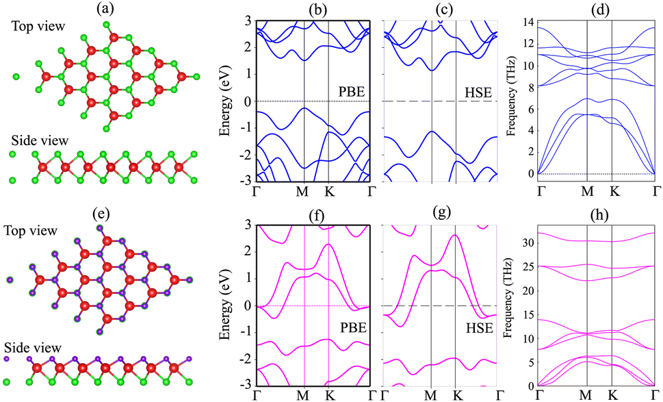 | ||
| Fig. 1 Atomic structures, band structures and phonon spectra of (a–d) MoS2 and (e–h) MoSH monolayers. | ||
We proceed with constructing the atomic structures of the metal–semiconductor heterojunction by combining metallic MoSH with semiconducting MoS2. The atomic configurations of the MoSH@MoS2 heterostructure are depicted in Fig. 2. The construction of the MoSH@MoS2 heterostructure involves maintaining the fixed lattice parameters of both MoSH and MoS2 monolayers. The resulting lattice constant of the MoSH@MoS2 heterostructure is determined to be 3.085 Å, representing the average of the lattice parameters of the individual monolayers. This indicates the presence of strain when the two materials are combined in the heterostructure. The lattice mismatch between the two monolayers in the heterostructure is calculated to be 2.75%, which is relatively small and has a negligible impact on the main properties of the materials. The formation of the MoSH@MoS2 heterostructure gives rise to the establishment of two distinct alignment configurations, namely MoSH@MoS2 and MoHS@MoS2 heterostructures. Each configuration consists of two different stacking patterns known as AA and AB stacking patterns, which are illustrated in Fig. 2(a) and (b). After the geometric optimization, the interlayer spacings d between two materials are obtained to be 2.79/2.86 Å for MoSH@MoS2 with the AB/AA stacking pattern and 3.53/3.54 Å for MoHS@MoS2 with the AB/AA stacking pattern. One can find that the interlayer spacing in the MoSH@MoS2 configuration is shorter than that in the MoHS@MoS2 configuration. This can be attributed to the weaker electronegativity of hydrogen atoms compared to sulfur atoms.
 | ||
| Fig. 2 Atomic structures of (a) MoSH@MoS2 and (b) MoHS@MoS2 heterostructures for different stacking patterns of AA and AB. | ||
To determine the stability of the MoSH@MoS2 heterostructure, we further calculate the binding energy, which provides an estimate of the energy released when the heterostructure is formed, indicating the stability of the system. The binding energy (Eb) can be calculated using the following formula:
 | (1) |
We now calculate the projected band structures of both the MoSH@MoS2 and MoHS@MoS2 heterostructures for the AA and AB stacking patterns, as depicted in Fig. 3. Both the PBE and HSE functionals are used to predict the band structures of the heterostructure. Red and blue lines represent the contributions of Janus MoSH and MoS2 monolayers, respectively. We can find that all four stacking patterns show metallic characteristics. Furthermore, the combination between metallic MoSH and semiconducting MoS2 layers results in the generation of a metal/semiconductor heterojunction. This results in the possibility of forming either a Schottky or an ohmic contact, depending on the relative position of the band edges of the semiconducting MoS2 layer with respect to the Fermi level (EF). All the stacking patterns of the MoSH@MoS2 and MoHS@MoS2 heterostructures generate Schottky contact (ShC). The ShC in heterostructure is measured using the Schottky barrier height (SBH) which can be calculated using the following formula:
| Φn = ECBM − EF | (2) |
| Φp = EF − EVBM | (3) |
 | ||
| Fig. 3 Projected band structures by PBE and HSE calculations of MoSH@MoS2 for (a) AA and (b) AB stacking patterns and MoHS@MoS2 for (c) AA and (d) AB stacking patterns. Red and green lines represent the contributions of MoSH and MoS2 layers, respectively. | ||
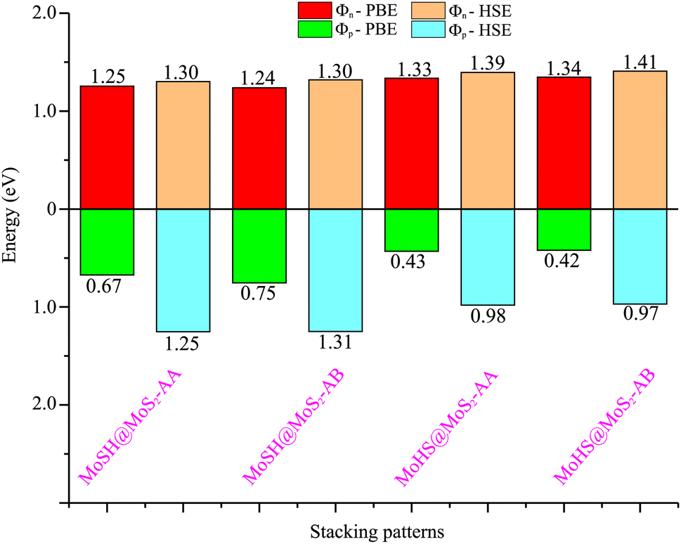 | ||
| Fig. 4 Calculated SBHs of the heterostructures between MoSH and MoS2 monolayers for different configurations using PBE and HSE functionals. | ||
Based on our previous discussion, it is evident that the AB stacking pattern is more favorable and stable than the AA stacking pattern for both the MoSH@MoS2 and MoHS@MoS2 heterostructures. The electrostatic potential and charge density differences (CDDs) of the MoSH@MoS2 and MoHS@MoS2 heterostructures for the AB stacking pattern are depicted in Fig. 5. Through the electrostatic potential of heterostructures, we can calculate the barrier height (hTB) and width (wTB) of the tunneling potential barrier. The calculated barrier height and width are 4.17 eV and 1.84 Å, respectively, for the MoSH@MoS2 heterostructure and are 4.87 eV and 2.06 Å, respectively, for the MoHS@MoS2 heterostructure. We further calculate the tunneling probability across the vdW interface, which can be obtained as follows:
 | (4) |
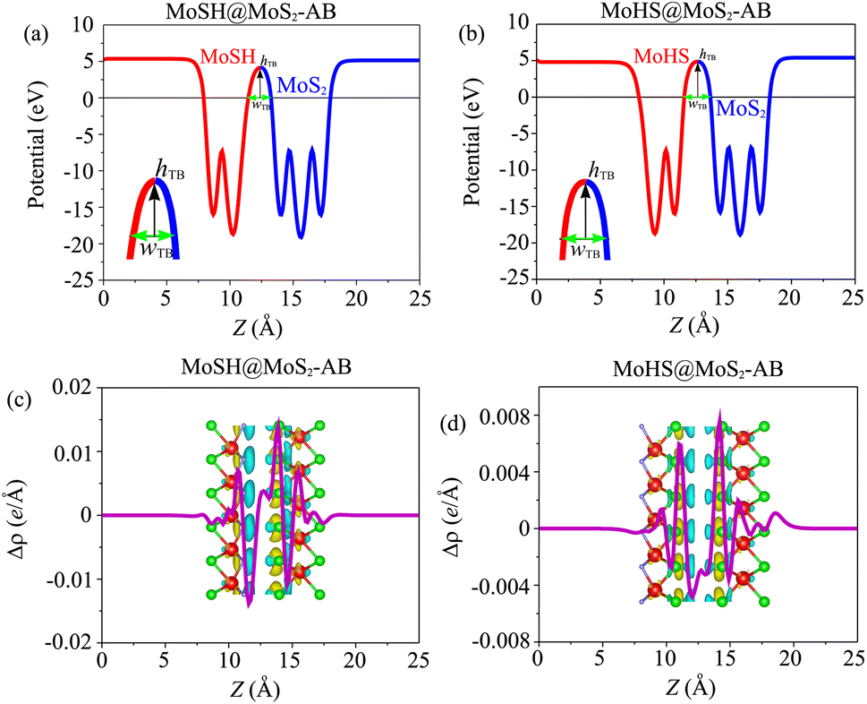 | ||
| Fig. 5 Electrostatic potential of (a) MoSH@MoS2 and (b) MoHS@MoS2 heterostructures for the AB stacking pattern. 2D planar-averaged charge density differences of (c) MoSH@MoS2 and (d) MoHS@MoS2 heterostructures for the AB stacking pattern. The yellow regions represent areas of charge accumulation, while the cyan regions indicate charge depletion. | ||
To gain a deeper understanding of the charge redistribution at the interface of the heterostructures, we plot the CDD of the heterostructure. The CDD represents the difference in charge density between the heterostructure and the isolated constituent layers, which can be visualized as follows:
| Δρ = ρH − ρMoSH − ρMoS2 | (5) |
To assess the tunability of the heterostructure under an applied electric field, we investigate the response of the MoSH@MoS2 heterostructure to varying electric field strengths. By studying the response of the MoSH@MoS2 heterostructure to different electric field strengths, we can gain insights into its adaptability and potential for use in various electronic and optoelectronic applications. As previously discussed, the AB stacking pattern of the MoSH@MoS2 heterostructure exhibits the highest SBH among the different stacking patterns. This indicates a relatively larger energy barrier for charge transfer at the metal/semiconductor interface. On the other hand, the AB stacking pattern of the MoHS@MoS2 heterostructure has the narrowest SBH among the different stacking patterns. This suggests a relatively easier charge transfer across the interface due to a smaller energy barrier. The SBH is an important parameter that determines the efficiency and nature of charge transfer at the metal/semiconductor interface, influencing the overall performance and functionality of electronic devices based on these heterostructures. A lower SBH between the metal and semiconductor interface typically leads to an enhanced flow of current, which can improve the performance of electronic devices. This reduced barrier allows for easier electron or hole injection and facilitates efficient charge transport across the interface. Consequently, a lower SBH is often desired for achieving higher device performance, such as improved conductivity and enhanced device efficiency. The MoHS@MoS2 heterostructure, with its low SBH of 0.42 eV, indicates promising potential for high-performance Schottky devices.
We now turn to investigate the possibility of adjusting the SBH under an applied electric field of the heterostructure with the largest SBH. By subjecting this heterostructure to different electric field strengths, we aim to explore whether the SBH can be modified and controlled. The schematic model of the applied electric field to the MoSH@MoS2 heterostructure is depicted in Fig. 6(a). With the application of the electric field, the SBH of the MoSH@MoS2 heterostructure is changed, as depicted in Fig. 6(b). The negative electric field gives rise to a decrease in the Φp, while the Φn increases correspondingly. The decrease in Φp suggests a reduction in the energy barrier for charge carrier injection from the metal to the semiconductor, potentially resulting in enhanced charge transport and an increased current flow. On the other hand, the positive electric field leads to an increase in the Φp, while the Φn has decreased accordingly. At a positive electric field strength of +0.6 V Å−1, an interesting phenomenon occurs in the MoSH@MoS2 heterostructure: the narrowing of the Schottky barrier height (Φn) relative to the Schottky barrier height (Φp). This observation suggests the possibility of a transition from p-type Schottky contact (ShC) to n-type ShC. The narrowing of Φn compared to Φp indicates that the energy barrier for charge extraction from the semiconductor to the metal decreases more significantly than the energy barrier for charge injection from the metal to the semiconductor. As a result, the heterostructure's electrical behavior shifts from favoring the injection of holes (p-type) to the injection of electrons (n-type). This transition from p-type ShC to n-type ShC is significant as it opens up new avenues for device functionality and performance. It enables the heterostructure to exhibit ambipolar behavior, where both electron and hole transport can be efficiently controlled, leading to enhanced device versatility and potential applications in areas such as electronic logic circuits and optoelectronic devices.
 | ||
| Fig. 6 (a) Schematic illustration of the applied electric field and (b) the fluctuation of the Schottky barrier of the MoSH@MoS2 heterostructure as a function of the electric field. | ||
In order to elucidate the underlying physical mechanism behind the changes in the SBH and contact types in the heterostructure, we plotted the projected band structure at various strengths of the electric field, as depicted in Fig. 7. Under the influence of a negative electric field, we observe distinct shifts in the band edges of the semiconducting MoS2 layers. Specifically, the VBM moves closer to the Fermi level, while the CBM moves further away from the Fermi level. These contrasting shifts in the band edges under a negative electric field contribute to the modification of the SBH and the resulting changes in the contact type in the heterostructure. Similarly, with the application of a positive electric field, the CBM of the semiconducting MoS2 shifts towards the Fermi level, while the VBM moves further away from the Fermi level. At a positive electric field of +0.6 V Å−1, the CBM of the semiconducting MoS2 layer is positioned closer to the Fermi level compared to its VBM. This arrangement indicates a transition from p-type ShC to n-type ShC. Furthermore, to gain a better understanding of the transition mechanism in the MoSH@MoS2 heterostructure, it is important to conduct either the crystal orbital Hamilton population (COHP) analysis 45,46 or the partial density of states (PDOS) analysis of all atoms, as depicted in Fig. 8. By analyzing the partial density of states (PDOS) of all atoms and each layer in the MoSH@MoS2 heterostructure, we can observe that the application of electric fields induces a shift in the band edges of the semiconducting MoS2 layer. Therefore, we can conclude that the applied electric field can be utilized to adjust both the SBH and contact types in the MoSH@MoS2 heterostructure. This capability to control the SBH and contact types through the application of an electric field provides opportunities for fine-tuning the electronic properties and performance of devices based on the MoSH@MoS2 heterostructure.
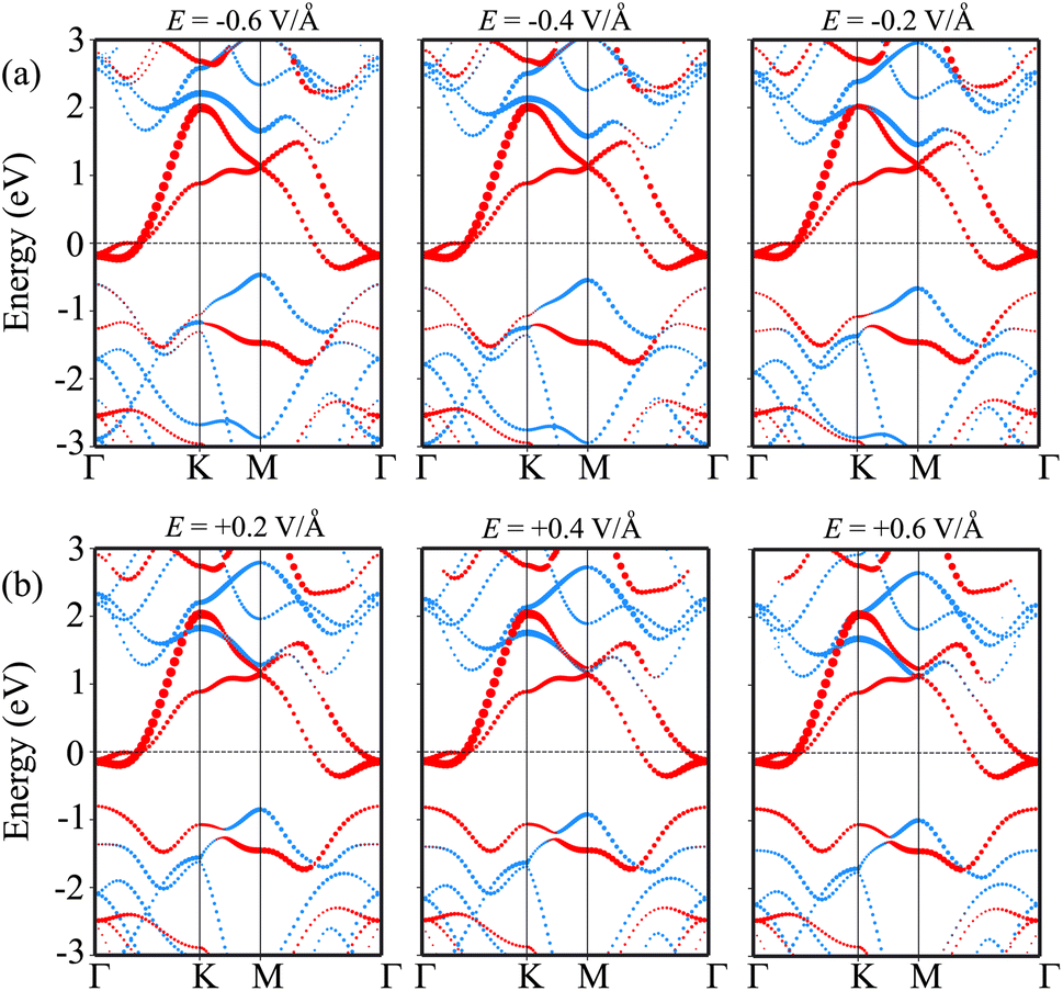 | ||
| Fig. 7 Projected band structures of the MoSH@MoS2 heterostructure for the AB pattern for different strengths of (a) negative and (b) positive electric fields. Red and green lines represent the contributions of MoSH and MoS2 layers, respectively. | ||
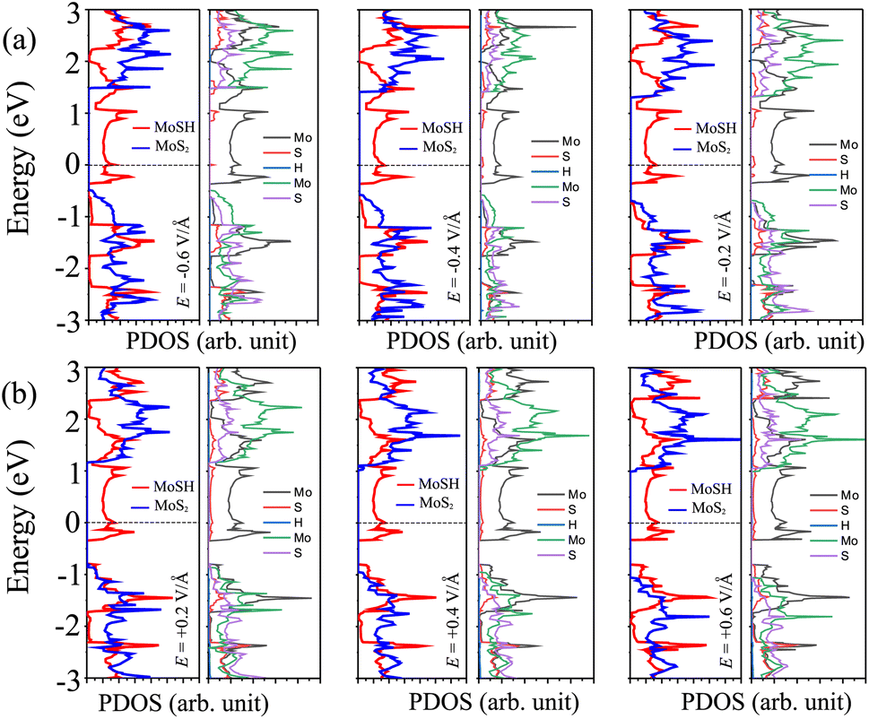 | ||
| Fig. 8 Projected density of states (PDOS) of Mo, S, and H atoms in the MoSH layer and Mo and S atoms in the MoS2 layer in the MoSH@MoS2 heterostructure under (a) applied negative and (b) positive electric fields. | ||
4. Conclusions
In conclusion, we have constructed a novel metal–semiconductor heterostructure between Janus MoSH and MoS2 monolayers and investigated its structures, electronic properties and the generation of Schottky contact using first-principles prediction. The effects of the electric field on controllable electronic properties and contact characteristics of MoSH@MoS2 heterostructures are also explored. Our findings show that the MoSH@MoS2 heterostructures exhibit p-type Schottky contact with different Schottky barrier heights, depending on the stacking configurations. The MoSH@MoS2 heterostructures possess low tunneling probabilities, indicating a relatively low electron transparency across all the patterns of the MoSH@MoS2 heterostructures. Furthermore, the applied electric field can be utilized to adjust both the SBH and contact types in the MoSH@MoS2 heterostructure. Our study sheds light on the potential applications of the MoSH@MoS2 heterostructure in electronic devices, demonstrating its tunability and versatility. This work contributes to the fundamental understanding of metal–semiconductor heterostructures and provides a foundation for further exploration and utilization of these materials in various technological applications.Data availability
The data that support the findings of this study are available from the corresponding author upon reasonable request.Conflicts of interest
There are no conflicts to declare.References
- K. S. Novoselov, A. Mishchenko, o. A. Carvalho and A. Castro Neto, Science, 2016, 353, aac9439 CrossRef CAS PubMed.
- G. Fiori, F. Bonaccorso, G. Iannaccone, T. Palacios, D. Neumaier, A. Seabaugh, S. K. Banerjee and L. Colombo, Nat. Nanotechnol., 2014, 9, 768–779 CrossRef CAS PubMed.
- P. Miró, M. Audiffred and T. Heine, Chem. Soc. Rev., 2014, 43, 6537–6554 RSC.
- A. C. Neto, F. Guinea, N. M. Peres, K. S. Novoselov and A. K. Geim, Rev. Mod. Phys., 2009, 81, 109 CrossRef.
- K. F. Mak, C. Lee, J. Hone, J. Shan and T. F. Heinz, Phys. Rev. Lett., 2010, 105, 136805 CrossRef PubMed.
- Y. Wu, C. He and W. Zhang, J. Energy Chem., 2023, 82, 375–386 CrossRef CAS.
- C. He, J. Ma, Y. Wu and W. Zhang, J. Energy Chem., 2023, 84, 131–139 CrossRef CAS.
- C. He, Z. Qi and W. Zhang, J. Alloys Compd., 2023, 934, 167786 CrossRef CAS.
- C. He, Y. Liang and W. Zhang, ACS Appl. Mater. Interfaces, 2022, 14, 29120–29130 CrossRef CAS PubMed.
- J. An, X. Zhao, Y. Zhang, M. Liu, J. Yuan, X. Sun, Z. Zhang, B. Wang, S. Li and D. Li, Adv. Funct. Mater., 2022, 32, 2110119 CrossRef CAS.
- J. Shim, H.-Y. Park, D.-H. Kang, J.-O. Kim, S.-H. Jo, Y. Park and J.-H. Park, Adv. Electron. Mater., 2017, 3, 1600364 CrossRef.
- B. Xu, S. Qi, M. Jin, X. Cai, L. Lai, Z. Sun, X. Han, Z. Lin, H. Shao and P. Peng, et al. , Chin. Chem. Lett., 2019, 30, 2053–2064 CrossRef CAS.
- H. Tao, Q. Fan, T. Ma, S. Liu, H. Gysling, J. Texter, F. Guo and Z. Sun, Prog. Mater. Sci., 2020, 111, 100637 CrossRef CAS.
- S. Yang, C. Jiang and S.-h. Wei, Appl. Phys. Rev., 2017, 4, 021304 Search PubMed.
- C. Anichini, W. Czepa, D. Pakulski, A. Aliprandi, A. Ciesielski and P. Samorì, Chem. Soc. Rev., 2018, 47, 4860–4908 RSC.
- A. K. Geim and I. V. Grigorieva, Nature, 2013, 499, 419–425 CrossRef CAS PubMed.
- C. Jin, E. Y. Ma, O. Karni, E. C. Regan, F. Wang and T. F. Heinz, Nat. Nanotechnol., 2018, 13, 994–1003 CrossRef CAS PubMed.
- C. Gong, E. M. Kim, Y. Wang, G. Lee and X. Zhang, Nat. Commun., 2019, 10, 2657 CrossRef PubMed.
- Y. Kim, A. R. Kim, J. H. Yang, K. E. Chang, J.-D. Kwon, S. Y. Choi, J. Park, K. E. Lee, D.-H. Kim and S. M. Choi, et al. , Nano Lett., 2016, 16, 5928–5933 CrossRef CAS PubMed.
- Y. Liu, P. Stradins and S.-H. Wei, Sci. Adv., 2016, 2, e1600069 CrossRef PubMed.
- Y. Sata, R. Moriya, S. Morikawa, N. Yabuki, S. Masubuchi and T. Machida, Appl. Phys. Lett., 2015, 107, 023109 CrossRef.
- J. Azadmanjiri, V. K. Srivastava, P. Kumar, Z. Sofer, J. Min and J. Gong, Appl. Mater. Today, 2020, 19, 100600 CrossRef.
- E. Lee, S. G. Lee, W. H. Lee, H. C. Lee, N. N. Nguyen, M. S. Yoo and K. Cho, Chem. Mater., 2020, 32, 4544–4552 CrossRef CAS.
- R. Munoz, E. López-Elvira, C. Munuera, R. Frisenda, C. Sánchez-Sánchez, J. Á. Martín-Gago and M. García-Hernández, Appl. Surf. Sci., 2022, 581, 151858 CrossRef CAS.
- D. M. Seo, J.-H. Lee, S. Lee, J. Seo, C. Park, J. Nam, Y. Park, S. Jin, S. Srivastava and M. Kumar, et al. , ACS Photonics, 2019, 6, 1379–1386 CrossRef CAS.
- P. Zhang, C. Bian, J. Ye, N. Cheng, X. Wang, H. Jiang, Y. Wei, Y. Zhang, Y. Du and L. Bao, et al. , Sci. China Mater., 2020, 1548–1559 CrossRef CAS.
- Y. Shu, K. He, R. Xiong, Z. Cui, X. Yang, C. Xu, J. Zheng, C. Wen, B. Wu and B. Sa, Appl. Surf. Sci., 2022, 604, 154540 CrossRef CAS.
- C. V. Nguyen, Phys. Rev. B, 2021, 103, 115429 CrossRef CAS.
- C. V. Nguyen, M. Idrees, H. V. Phuc, N. N. Hieu, N. T. Binh, B. Amin and T. V. Vu, Phys. Rev. B, 2020, 101, 235419 CrossRef CAS.
- S.-T. Nguyen, P. V. Cuong, C. Q. Nguyen and C. V. Nguyen, Phys. Chem. Chem. Phys., 2022, 24, 25144–25150 RSC.
- X. Wan, E. Chen, J. Yao, M. Gao, X. Miao, S. Wang, Y. Gu, S. Xiao, R. Zhan and K. Chen, et al. , ACS Nano, 2021, 15, 20319–20331 CrossRef CAS PubMed.
- R. Ku, L. Yan, J.-G. Si, S. Zhu, B.-T. Wang, Y. Wei, K. Pang, W. Li and L. Zhou, Phys. Rev. B, 2023, 107, 064508 CrossRef CAS.
- P.-F. Liu, F. Zheng, J. Li, J.-G. Si, L. Wei, J. Zhang and B.-T. Wang, Phys. Rev. B, 2022, 105, 245420 CrossRef CAS.
- Y.-P. He, S.-Y. Wu, J.-X. Guo, Q.-H. Qiu and T.-H. Guo, Philos. Mag., 2023, 1–15 Search PubMed.
- J. Wang, L. Bai, X. Zhao, C. Chen and L. Niu, Phys. E, 2023, 149, 115668 CrossRef CAS.
- C. V. Nguyen, C. Q. Nguyen, S.-T. Nguyen, Y. S. Ang and N. V. Hieu, J. Phys. Chem. Lett., 2022, 13, 2576–2582 CrossRef CAS PubMed.
- P. Giannozzi, S. Baroni, N. Bonini, M. Calandra, R. Car, C. Cavazzoni, D. Ceresoli, G. L. Chiarotti, M. Cococcioni and I. Dabo, et al. , J. Phys.: Condens.Matter, 2009, 21, 395502 CrossRef PubMed.
- P. Giannozzi, O. Andreussi, T. Brumme, O. Bunau, M. B. Nardelli, M. Calandra, R. Car, C. Cavazzoni, D. Ceresoli and M. Cococcioni, et al. , J. Phys.: Condens.Matter, 2017, 29, 465901 CrossRef CAS PubMed.
- J. P. Perdew, K. Burke and M. Ernzerhof, Phys. Rev. Lett., 1996, 77, 3865 CrossRef CAS PubMed.
- P. E. Blöchl, Phys. Rev. B: Condens. Matter Mater. Phys., 1994, 50, 17953 CrossRef PubMed.
- S. Grimme, J. Antony, S. Ehrlich and H. Krieg, J. Chem. Phys., 2010, 132, 154104 CrossRef PubMed.
- J. Heyd, G. E. Scuseria and M. Ernzerhof, J. Chem. Phys., 2003, 118, 8207–8215 CrossRef CAS.
- L. Li, T. Huang, K. Liang, Y. Si, J.-C. Lian, W.-Q. Huang, W. Hu and G.-F. Huang, Phys. Rev. Appl., 2022, 18, 014013 CrossRef CAS.
- K. Liang, T. Huang, K. Yang, Y. Si, H.-Y. Wu, J.-C. Lian, W.-Q. Huang, W.-Y. Hu and G.-F. Huang, Phys. Rev. Appl., 2021, 16, 054043 CrossRef CAS.
- Y. Wu, C. He and W. Zhang, J. Am. Chem. Soc., 2022, 144, 9344–9353 CrossRef CAS PubMed.
- Y. Wu, C. He and W. Zhang, ACS Appl. Mater. Interfaces, 2021, 13, 47520–47529 CrossRef CAS PubMed.
| This journal is © The Royal Society of Chemistry 2023 |