
 Open Access Article
 This Open Access Article is licensed under a Creative Commons Attribution-Non Commercial 3.0 Unported Licence
Engineering GaN/AuNC core–shell nanowire heterojunctions by gold nanoclusters with excitation-dependent behavior for enhancing the responsivity and stability of self-driven photodetectors†
Yuanyuan
Huang
a,
Jianya
Zhang
bc,
Min
Zhou
d,
Renjun
Pei
*ad and
Yukun
Zhao
 *cd
*cd
aCAS Key Laboratory for Nano-Bio Interface, Suzhou Institute of Nano-Tech and Nano-Bionics (SINANO), Chinese Academy of Sciences (CAS), Suzhou, 215123, China. E-mail: rjpei2011@sinano.ac.cn
bJiangsu Key Laboratory of Micro and Nano Heat Fluid Flow Technology and Energy Application, School of Physical Science and Technology, Suzhou University of Science and Technology, Suzhou, 215009, China
cKey Lab of Nanodevices and Applications, Suzhou Institute of Nano-Tech and Nano-Bionics (SINANO), Chinese Academy of Sciences (CAS), Suzhou, 215123, China. E-mail: ykzhao2017@sinano.ac.cn
dSchool of Nano-Tech and Nano-Bionics, University of Science and Technology of China, Hefei, 230026, China
First published on 23rd October 2023
Abstract
Self-driven broadband photodetectors (PDs) with low-power consumption have great potential applications in the wide range of next-generation optoelectronic devices. In this study, a self-driven broadband PD responding to an ultraviolet-visible range based on gallium nitride/gold nanocluster (GaN/AuNC) core–shell nanowire heterojunctions is fabricated for the first time. By introducing the AuNCs onto the GaN nanowire surfaces, the GaN/AuNC core–shell nanowire heterojunctions can be formed efficiently. It is crucial that AuNCs have the functions of light collectors and hole conductors in heterojunctions due to the suitable energy level alignment. Under the optimized conditions of AuNCs, it is found that GaN/AuNC core–shell nanowires can significantly increase the photocurrent and responsivity of PDs, mainly resulting from the light interreflection within the heterojunctions and the effective improvement of carrier transport. Owing to the excitation-dependent emission behavior of AuNCs, the responsivity of PD with GaN/AuNC core–shell nanowire heterojunctions can be enhanced by around 330% compared with that of PD without AuNCs under visible illumination. Furthermore, GaN/AuNC hybrid nanowires with excitation-dependent fluorescence behavior can modulate the enhanced amplitude performance of broadband PDs. Owing to the high stability of AuNCs, the photocurrent of the PD with AuNCs is still quite stable after continuous operation for more than 20![[thin space (1/6-em)]](https://www.rsc.org/images/entities/char_2009.gif) 000 s. Therefore, this study provides an effective method for developing new broadband PDs with high performance and low energy consumption.
000 s. Therefore, this study provides an effective method for developing new broadband PDs with high performance and low energy consumption.
1. Introduction
Without having to provide an external power supply, self-driven photodetectors (PDs) play an increasingly important role in photoelectric sensing and high-performance communication systems.1–6 Owing to the merits of inexpensive and self-powered supply, photoelectrochemical (PEC) PD can broaden the PD applications in various fields.2,7–10 Furthermore, ultraviolet (UV) PDs have aroused great concern because they can be used in the fields of ozone sensing, flame detectors, communication service and UV astronomy.11–19 Hence, PEC UV PDs have been attractive and identified as candidates suited for a wide range of applications with low-power consumption.Compared with PDs responding to the specific wavelength range, broadband PDs are operated over a much wider wavelength region and have attracted significant attention in various applications, such as expanding optical communication capabilities and multispectral imagery.20–22 Because the UV-visible (UV-Vis) range is the major part of the solar spectrum, high-performance UV-Vis PDs are worth exploring.23 Thus, developing novel materials is still very demanding and challenging for fabricating UV-Vis PDs with high stability and low-power consumption.23–25
Gallium nitride (GaN) material is promising for fabricating self-driven PEC UV PDs because it has the extraordinary characteristics of a wide energy bandgap to absorb UV photons, as well as the high stability for withstanding the electrochemical (EC) etching and radiation.26 Because nanowires (NWs) can have a high surface-to-volume ratio and optical absorption, GaN NWs are suitable for application in PEC UV PDs.27,28 However, the responsivity and narrowband of GaN-based PDs are still pretty influenced and limited, which obstruct their development significantly, especially in Vis PDs.29–31
In our previous study, it was found that all-inorganic halide perovskites [e.g. cesium lead bromide (CsPbBr3)] can enhance the photocurrent and responsivity of UV PDs.32 However, CsPbBr3 is well known to be unstable owing to its rapid degradation in water. In the PEC detection, the PD photocurrent decreases obviously after only half an hour.32 Thus, although CsPbBr3 material has landmark optoelectronic properties, the poor stability is a key problem deteriorating the device performance.32,33 Owing to their distinct properties, including their self-assembling nature, strong luminescence and charge storage capability, the molecule-like noble metal nanoclusters have been investigated.34 Recently, metal nanocluster-based hybrid nanomaterials have been fabricated for sensing, biomedicine, catalytic and LED applications, which could utilize the distinctive photoelectrical properties of metal nanoclusters.35 However, gold nanoclusters (AuNCs) have been designed only for a specific wavelength range, not for broadband photoresponse.33,36,37 Considering the excellent optoelectronic properties of both AuNCs and GaN NWs, and the research vacancy of AuNC hybrid GaN-based PDs, it is still challenging and attractive to combine AuNCs with GaN NWs to increase the responsivity of UV-Vis PDs significantly.
In this study, a PEC broadband PD that responds to a wide wavelength region from the UV to the Vis range is fabricated based on vertical GaN NWs and AuNCs without complicated processes. In contrast to the single emissive wavelength of AuNCs, specific ligand-protected AuNCs with excitation-dependent emission behavior are designed for tunable luminescence. By introducing AuNCs into the Si-based GaN NWs, GaN/AuNC hybrid NWs are successfully prepared with red-shifted luminescence from 520 nm to 730 nm as the excitation wavelength increases from 405 to 620 nm. Importantly, GaN/AuNC hybrid NWs can enhance the photocurrent and responsivity of PDs with a broadband UV-Vis photoresponse from 405 nm to 620 nm. Furthermore, the stability and fundamental mechanisms of GaN/AuNC core–shell NW heterojunctions have been investigated systematically.
2. Experimental section
2.1. Fabrication of GaN NWs
Molecular beam epitaxy (MBE, Vecco G20) was utilized to prepare the GaN NWs (Fig. 1a). Before MBE growth, 2-inch n-type Si(111) substrates were heated up to 900 °C for about 15 min to eliminate native oxides. In the growth chamber with the Ga effusion cell and an N plasma cell, the substrate temperature was set to 830 °C. We grew GaN NWs with a Ga flux of ∼4.0 × 10⁻⁸ Torr for about 100 min without doping. The nitrogen flow rate and plasma power were 4.8 sccm and 450 W, respectively.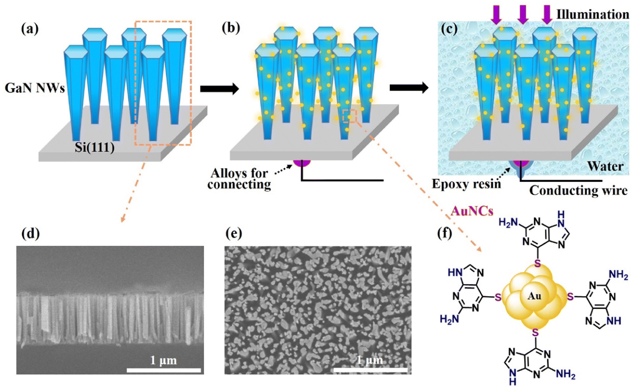 | ||
| Fig. 1 (a) Grow the GaN NWs on the Si substrate using MBE. (b) Coat the AuNCs onto the NW surfaces and connect the conducting wire. (c) Measure the PD under illumination. (d) Side-view and (e) top-view scanning electron microscopy (SEM) images of GaN NWs. (f) Schematic structure of AuNC crystals. | ||
2.2. Preparation of AuNCs
The prepared AuNCs were fabricated by applying a one-step synthesis method using 6-thioguanine as a reducing agent and stabilizing ligand. The 6-thioguanine solid (38 mg) in pure water and methanol was adjusted to alkalinity to obtain a transparent solution. Then, the HAuCl4 (52 mM, 550 μL) aqueous solution was added dropwise into the 6-thioguanine solutions under vigorous stirring for 3 days. The formation of a turbid solution emitted green luminescence under UV lamp irradiation (365 nm), suggesting the successful synthesis of AuNCs. The precipitates were collected by centrifugation and desiccation, which were further ground to obtain the AuNC powders and could be kept for long-term preservation at room temperature because of their good stability.2.3. Fabrication of self-driven PEC PDs with GaN/AuNC hybrid NWs
The as-grown GaN NW samples were divided into small pieces. Then, In/Au/Al alloys were melted on the back side of the Si substrate using an electric soldering iron coated with epoxy resin to avoid leakage current and EC corrosion (Fig. 1b and c). During the underwater measurements, the NW sample and Pt plate were used as working and counter electrodes. To introduce AuNCs, we applied a dimethyl sulfoxide (DMSO) droplet with AuNCs (2 mg mL−1) onto the surfaces of GaN NWs (Fig. 1b). GaN NW and AuNCs were designed and fabricated to be the core and shell, respectively, leading to the formation of GaN/AuNC NW heterojunction. This procedure can avoid the effects of high-temperature processes on AuNCs and keep them stable. Table 1 shows some details of the two samples used in this study.| Sample | Material | PEC PD |
|---|---|---|
| PD | GaN NWs | Yes |
| PD with AuNCs | GaN NWs + AuNCs | Yes |
2.4. Characterization and measurements
To characterize the morphology and element distribution of NWs and AuNCs, scanning electron microscopy (SEM, S-4800, HITACHI) and spherical aberration-corrected scanning transmission electron microscope (AC-STEM, Themis Z, FEI) with a high-resolution energy dispersive X-ray (EDX) mapping were utilized in this study. A focused ion beam (FIB, Scios, FEI) was utilized to prepare the STEM samples. The UV-Vis absorption spectra were recorded using a 1280 UV-Visible spectrophotometer (Shimadzu, Japan). The luminescence spectra were obtained using an F-4600 fluorescence spectrometer. X-ray photoelectron spectroscopy (XPS) was recorded using a Thermo Scientific K-Alpha spectrometer.An EC workstation in the PEC system (DH 7000, Jiangsu Donghua Analytical Instrument, Co., Ltd) was used to evaluate the electrical properties of the PDs in a reaction vessel with an electrolyte of pure water (Fig. 1c). Except for the current–voltage (I–V) measurements, the PD characteristics were all measured at 0 V bias. To make the comparison of PD performance more accurate, PD without AuNCs was first characterized. Then, we fabricated and measured the PDs with AuNCs based on the corresponding PDs without AuNCs. This is an effective way to eliminate the differences between PDs with different NWs.
3. Results and discussion
Fig. 1a–c schematically shows the preparation processes of PD with AuNCs. For better comparison in this study, the PD without AuNCs is regarded as “PD”, while the PD with GaN/AuNC hybrid NWs is regarded as “PD with AuNCs”. As illustrated in Fig. 1d, e and S1,† the grown NWs exhibit good verticality and uniformity. The heights of the NWs are about 670 nm, and the diameter ranges from 20 nm to 40 nm. Fig. 1f shows the schematic structure of AuNC crystals with 6-thioguanine as a reducing agent and stabilizing ligand, which contains the dominating elements of Au, S, C and N.From Fig. S2a,† the entire X-ray photoelectron spectroscopy (XPS) spectrum of GaN/AuNC hybrid NWs shows the expected constituent elements of Ga, Au, S, C and N, indicating the successful hybrid between GaN and AuNCs. The binding energies of Au 4f at 84.7 eV and 88.3 eV correspond with Au 4f7/2 and Au 4f5/2, respectively (Fig. 2a). The characteristic peaks of Au 4f in GaN/AuNC hybrid NWs are consistent with previous AuNCs, suggesting the unchanged gold element.33 Furthermore, the binding energies of Ga 3d and N 1s display that the Ga–N, Ga–Ga, Ga–O, N![[double bond, length as m-dash]](https://www.rsc.org/images/entities/char_e001.gif) C and N–Ga bonds exist in the GaN/AuNC hybrid NWs (Fig. 2b and S2b†). As shown in Fig. 2b, the emergence of oxygen elements is usually attributed to unintentional doping during the growth process and the oxidation of the NW surface in air. However, the peak intensity of Ga–N is much higher than that of Ga–O, proving that GaN is the dominant material within the NWs. The N 1s spectrum depicted in Fig. S2b† can be deconvoluted into several peaks corresponding to the Ga LMM Auger transitions, bonds of N–Ga, NC, and N–C from low to high binding energies.38
C and N–Ga bonds exist in the GaN/AuNC hybrid NWs (Fig. 2b and S2b†). As shown in Fig. 2b, the emergence of oxygen elements is usually attributed to unintentional doping during the growth process and the oxidation of the NW surface in air. However, the peak intensity of Ga–N is much higher than that of Ga–O, proving that GaN is the dominant material within the NWs. The N 1s spectrum depicted in Fig. S2b† can be deconvoluted into several peaks corresponding to the Ga LMM Auger transitions, bonds of N–Ga, NC, and N–C from low to high binding energies.38
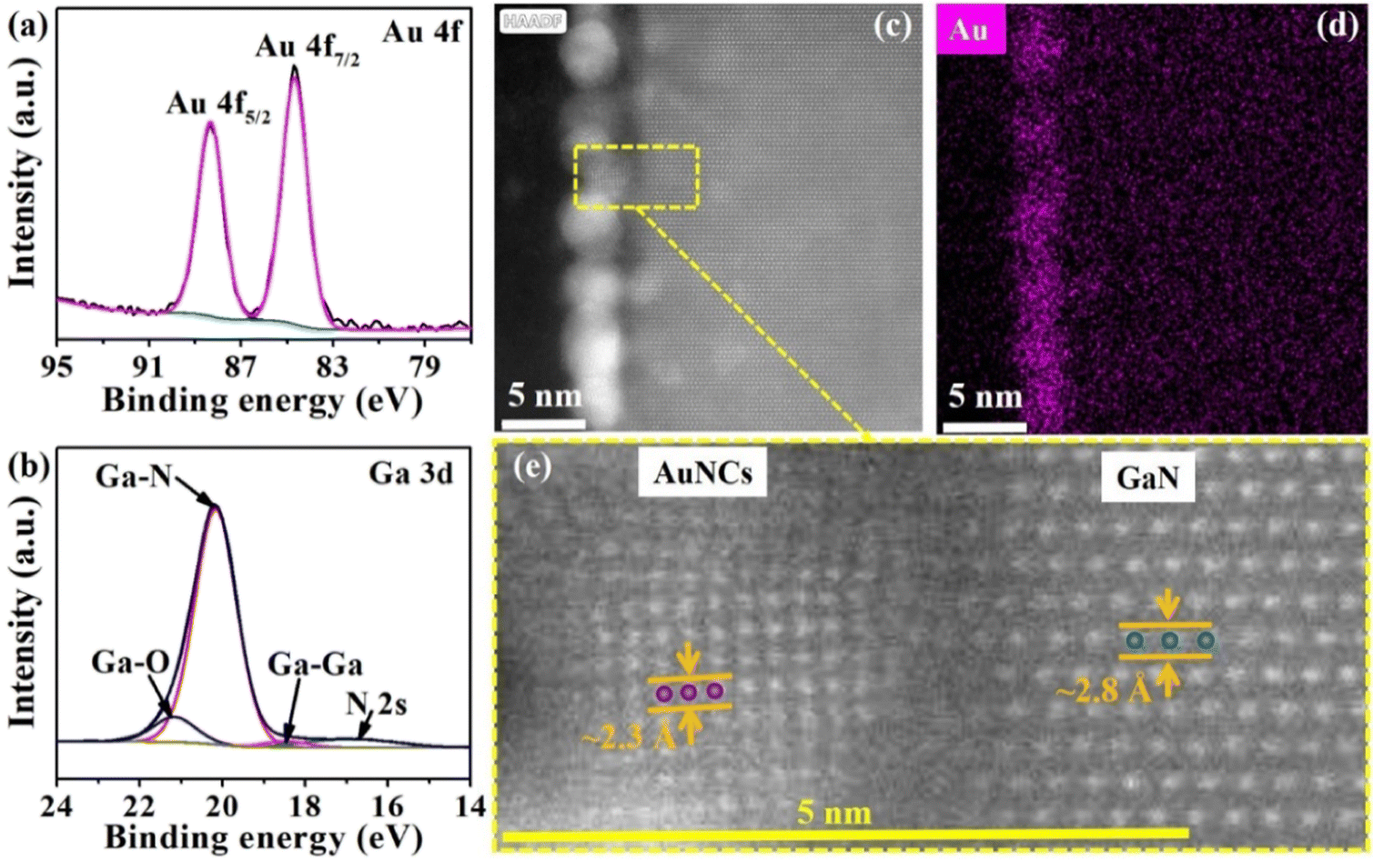 | ||
| Fig. 2 (a) Au 4f XPS spectrum and (b) Ga 3d XPS spectrum of GaN/AuNC hybrid NWs. (c) Side-view STEM and (d) the corresponding high-resolution EDX elemental mapping of a GaN/AuNC hybrid NW. (e) AC-STEM images of the GaN and AuNC crystals. | ||
To characterize the GaN/AuNC NW heterojunction and atomic layers clearer, the results of spherical aberration-corrected scanning transmission electron microscope (AC-STEM) with a high-resolution energy dispersive X-ray (EDX) mapping are shown in Fig. 2c–e, S3 and S4.† They indicate that AuNCs with an average size of about 3.4 nm are attached to the NW surface by serving as shells successfully, which is in good agreement with the experimental design illustrated in Fig. 1b. Owing to the van der Waals forces, AuNCs can be connected to the core of GaN NWs (Fig. S1, S3 and S4†). The shell of AuNCs seems continuous because of its high density. As illustrated in Fig. 2e, the lattice fringe spacing of AuNCs in GaN/AuNC hybrid NWs is measured as 2.3 Å owing to the (111) lattice spacing of the face-centered cubic Au.39 The spacing of the two atoms of GaN along the vertical direction is measured as around 2.8 Å.32 Such clear lattice spacing and fringe are observed in the AC-STEM image, suggesting good crystallinity in the wurtzite nitride binaries of GaN crystals. As depicted in Fig. 1f, S2a and S4,† the crystal of AuNCs contains more atoms of different elements (Ga, Au, S, C and N) than that of GaN (Ga and N), leading to a more complex crystal structure. Therefore, the dark region between AuNCs and GaN is proposed as the buffer area for coupling different crystals. The successful connection of GaN/AuNC crystals is extremely beneficial for carrier transport.
To explore the optical properties of AuNCs, the photoluminescence (PL) spectra are investigated, as shown in Fig. S5.† It is found that the maximum emission peak of pure AuNCs exhibits the bathochromic shift by changing the excitation wavelength from 405 to 620 nm (Fig. S5a†), displaying the typical excitation-dependent emission characteristics.40 Furthermore, the PL spectral peaks of GaN/AuNC hybrid NWs in Fig. 3a show the gradual red-shifted behavior of excitation-dependent emission from 520 nm to 730 nm by increasing the excitation wavelength from 405 to 620 nm. The emission spectral shapes of GaN/AuNC hybrid NWs exhibit better performance than those of pure AuNCs, suggesting the impact of the NW structure on the emission of AuNCs. The corresponding colors are displayed in the Commission International de I'Eclairage (CIE) chromaticity diagram, which indicates that GaN/AuNC hybrid NWs could achieve multicolor tunable luminescence (Fig. S6†). In addition, the excitation spectra of GaN/AuNC hybrid NWs in Fig. 3b are red-shifted from 405 nm to 620 nm along with the emission wavelengths ranging from 520 to 730 nm, suggesting the existence of various excited states.41 However, inconspicuous emission peaks of pure GaN NWs are observed under the same excitation wavelengths with GaN/AuNC hybrid NWs (Fig. S5b†). It can be confirmed that the prepared AuNCs endow the GaN/AuNC hybrid NWs with the unique property of excitation-dependent emission and eliminate the interference of GaN NWs. The as-prepared AuNCs are formed by internal hydrogen-bonded motifs with abundant acceptor and donor sites in the 6-thioguanine ligand, which generates the radiation relaxation of the metal-center triplet state through the charge transfer between the sulfur atoms of the ligand and gold atoms.42–44 The concerned mechanism for the excitation-dependent emission behavior of AuNCs is approximately proposed, as shown in Fig. 3c. The tunable PL peaks in the dried AuNCs on PD originate from the formation of multiple emissions through multichannel radiative relaxation processes by various energy excitations, which is mainly attributed to the different emissive trap sites, sizes, surface states or metallophilic interactions in AuNCs.40,41,45,46
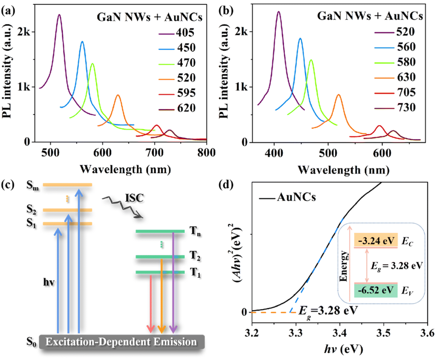 | ||
| Fig. 3 (a) Emission spectra of GaN/AuNC hybrid NWs under different excitation wavelengths ranging from 405 nm to 620 nm. (b) Excitation spectra of GaN/AuNC hybrid NWs under different emission wavelengths ranging from 520 nm to 730 nm. (c) Proposed mechanism for excitation-dependent emission of AuNCs, where S0, Sm and Tn represent the ground state, upper-excited singlet state and upper-excited triplet state, respectively. ISC represents the intersystem crossing process. (d) Energy bandgap value of AuNCs in DMSO solution calculated from the UV-Vis absorption spectra. Inset: the energy band diagram of AuNCs. | ||
As illustrated in Fig. S7a,† the UV-Vis absorption spectra of AuNCs in DMSO solution display a characteristic peak at about 346 nm, whereas the absorption from 750 nm to 400 nm is inconspicuous. The energy bandgap (Eg) value is estimated using the Tauc plot in Fig. 3d, which is calculated using the following equation:47,48
| (αhν)n = B(hν − Eg), | (1) |
Compared with the emission spectrum of pure GaN, the emission spectrum of GaN with AuNCs exhibits a red shift (Fig. S7b†). Owing to the photogenerated carriers, the photocurrent data of both PDs without and with AuNCs display ordered on–off behavior (Fig. 4a), which are measured at 0 V bias. Fig. 4b demonstrates that the photocurrent density increases with the increase in incident light power. As the critical PD indexes, the photocurrent (Iphoto), responsivity (R) and external quantum efficiency (EQE) are, respectively, calculated using the following equations:3,7
| Iphoto = Ilight − Idark, | (2) |
| R = Iphoto/(SPD × Pinc), | (3) |
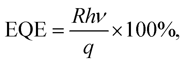 | (4) |
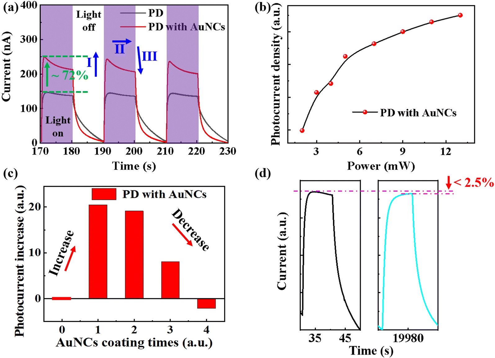 | ||
| Fig. 4 (a) Photo-switching behavior of PDs with and without AuNCs under 310 nm illumination. (b) Photocurrent at different incident light power densities. (c) Photocurrent variation trend of PDs with different coating times of AuNCs. (d) Long-time photocurrent behavior of the PD with AuNCs under 310 nm illumination. | ||
| Material | Wavelength (nm) | Responsivity (mA W−1) | EQE (%) | Long-time measurement (s) | Loss of photocurrent (%) | Reference |
|---|---|---|---|---|---|---|
| GaN NWs + CsPbBr3 | 310 | 1.08 | — | 10000 |
∼17 | 32 |
| (Al,Ga)N NWs:Ru | 254 | 48.8 | — | 600 | ∼10 (@0.4 V) | 7 |
| (In,Ga)N NWs + seawater | 490 | ∼1.8 | 0.46 | 9000 | ∼5 | 52 |
| GaN NWs + AuNCs | 310 | ∼1.9 | 0.77 | 20000 |
<2.5 | This work |
As clearly shown in Fig. 4c, we prepared more PD samples with different coating times for the AuNCs to further evaluate the influence of the AuNC quantities. The repeated droplet process was performed by drying the solution several times to coat the NW surfaces with more AuNCs. The PD with AuNCs in Fig. 4a and b were coated 1 time with AuNCs, while three more samples in Fig. 4c were prepared by coating 2, 3 and 4 times. The sample of PD without AuNCs was prepared by coating 0 time. Compared with the sample of PD without AuNCs, the photocurrent of PD with AuNCs coated 1–2 times is obviously enhanced. However, the photocurrent is obviously decreased when the amount of AuNCs continues to increase by coating more than 3 times. A video about how to operate the PEC system was shown in our previous study.51 Moreover, PD with AuNCs was utilized to study PD stability. As shown in Fig. 4d, the photocurrent decreases only slightly (<2.5%) despite the PD continuously working from 0 to ∼20000 s. Compared to that of the PDs with CsPbBr3, the photocurrent of the PD with AuNCs is much stabler (Table 2), which mainly results from the high stability of AuNCs.
The underlying mechanism in the PEC PDs is analysed by the schematic illustrations shown in Fig. 5. After absorbing the 310 nm photons, the photocarriers generated from both AuNCs and GaN NWs in the system of PDs with AuNCs are prone to form a photocurrent by transporting them through the GaN/AuNC core–shell NW heterojunctions (Fig. 5a and b). The present heterojunctions can offer both vertical and horizontal directions to the carrier transports (Fig. 5b), which are beneficial for absorbing photons and generating carriers owing to the large surface-to-volume ratio. Furthermore, the specific EC equilibrium could be achieved by transporting additional photocarriers from the NWs to the electrolyte under the condition of the GaN section contacting the electrolyte of water. The photogenerated current is probably generated according to the following reactions:53
| 4h+ + 2H2O = O2 + 4H+, | (5) |
| 4H+ + 4e− = 2H2. | (6) |
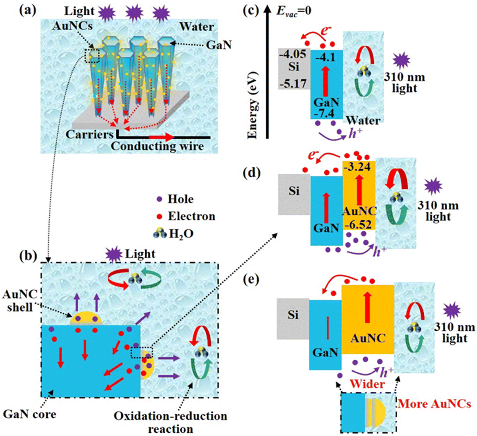 | ||
| Fig. 5 (a) Schematic illustration of the PD with AuNCs. (b) Enlarged schematic illustration of the GaN/AuNC core–shell NW heterojunction. Energy band diagrams of the PDs (c) without and (d) with AuNCs under 310 nm illumination. (e) Schematic illustration of GaN/AuNC core–shell NW heterojunction with many AuNCs and the corresponding energy band diagram under 310 nm illumination. | ||
The current is positively shifted under the condition that the light is on (process I in Fig. 4a). Under continuous exposure to illumination, the current density displays a trend of gentle decline until a new steady state (process II in Fig. 4a) is reached. The electrons generated by the photo are transferred to the conducting wire while holes are transferred to water (Fig. 5a). In the absence of external bias, the entire circuit can provide two functions of both light harvest and carrier transport, indicating self-driven characteristics. When the light is turned off (process III in Fig. 4a), the electrons that have accumulated within the semiconductor system are probably eliminated by the electron acceptor substances and recombined with trapped holes.54
The electronic affinity and energy band values illustrated in Fig. 5c–e come from ref. 44 and 55. Owing to the difference in work functions, the spontaneous formation of an internal electric field (i.e. built-in field) could be achieved.56,57 Under illumination of 310 nm, AuNCs can serve as hole conductor and light harvester.58 The energy of electrons in the EC of GaN is less than that of AuNCs, whereas the energy of holes in the EV of GaN is larger (Fig. 5d). Therefore, the introduction of AuNCs is beneficial for appropriate energy level alignment, which has the potential to accelerate carrier transport. Moreover, the interreflection between the NWs and AuNCs contributes to improving photon absorption and carrier generation,32 which is beneficial for enhancing photocurrent and responsivity (Fig. 4a). After coating several times with AuNCs on NW surfaces, too many AuNCs will likely be overlaid (Fig. 5e). This means that abundant AuNCs could broaden the corresponding transmission distance, which makes carrier transport difficult, and ultimately result in a decrease in the photocurrent. Therefore, AuNC quantity is an important parameter affecting PD performance.
According to the excitation-dependent emission behavior of PDs based on GaN NW-AuNC hybrid structures with red-shifted emission from 520 nm to 730 nm by increasing the excitation wavelength from 405 to 620 nm, the photocurrent and responsivity of PD with AuNCs at different wavelengths were investigated to explore the good stability of PDs. Under 470 nm illumination, both the photocurrent and responsivity of PD with AuNCs can be enhanced by around 330% compared with those of PD without AuNCs (Fig. 6a and S8a†). For the PD without AuNCs under 470 nm illumination, the photogenerated electron–hole pairs mainly come from the Si substrate because of the low-energy band gap (Fig. S8b†). Owing to the excitation-dependent fluorescence behavior, AuNCs can absorb Vis photons, increasing the efficiency of electron–hole separation and transport (Fig. 6b). In addition to light interreflection within GaN/AuNC core–shell NW heterojunctions, both photocurrent and responsivity are markedly increased in the Vis range. The enhancement of photocurrent caused by AuNCs is partly attributed to the strong local field enhancement around the AuNCs and the enhanced scattering of incident photons, which leads to the absorption of strong light around the AuNCs, resulting in an increase in photo-generated carriers.59 Simultaneously, the high catalytic activity of the modification of AuNCs helps drive photo-generated carriers to reach the redox reaction sites, thereby promoting carrier separation and reducing the surface photo corrosion of GaN NWs.7 Different from other AuNC-based PDs emitting single wavelength with gradually decreased photoresponse performance, GaN/AuNC hybrid NWs with excitation-dependent fluorescence behavior can regulate the enhanced amplitude performance of broadband PDs (Fig. 6a and Table S1†). Therefore, GaN/AuNC hybrid NWs can improve the performance of PDs with broadband UV-Vis photoresponse.
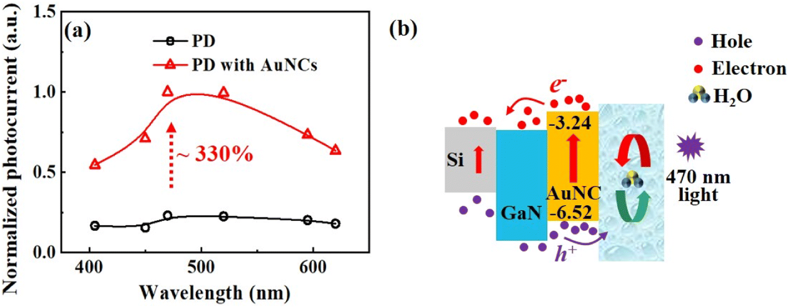 | ||
| Fig. 6 (a) Normalized photocurrent of PDs at different wavelengths. (b) Energy band diagram of the PD with AuNCs under 470 nm illumination. | ||
4. Conclusion
In summary, we fabricate a self-driven broadband PD that responds to the UV-Vis range based on GaN/AuNC core–shell NW heterojunctions successfully and economically. The formed GaN/AuNC core–shell NW heterojunction displays a good quality based on the distinct lattice spacing and fringes of AuNCs and GaN crystals. The successful connection of GaN/AuNC crystals is essential for carrier transport. The introduced AuNCs could work as both light harvesters and hole conductors in the PDs by producing a built-in electric field and configuring appropriate energy level alignment. It is found that GaN/AuNC core–shell nanowires with an appropriate quantity of AuNCs can significantly enhance the photocurrent and responsivity of broadband PDs. The key reasons are proposed to be the light interreflection within heterojunctions, the increased carrier transport and the excitation-dependent emission behavior of AuNCs. Compared with that of PD without AuNCs, the photoresponse performance of PD with AuNCs can be significantly increased under the irradiation wavelength from UV to Vis. Particularly, the responsivity of PD with AuNCs can be enhanced by around 330% compared to that of PD without AuNCs under 470 nm illumination. Many AuNCs can decrease the photocurrent because they can lengthen the path of carrier transport, and the quantity of AuNCs is a key factor affecting the performance of PDs with GaN/AuNC heterojunctions. Moreover, owing to the high stability of both AuNCs and GaN NWs, the photocurrent of PD decreases only slightly (<2.5%) after continuously working for ∼20000 s. Therefore, such design and demonstration of GaN/AuNC core–shell NW heterojunctions have the reference significance to further improve the PD performance within the broadband range and develop new PDs with high stability and low-power consumption.
Author contributions
Y. Y. H. and J. Y. Z. contributed equally to this work. Y. K. Z. conceived the idea and designed the research. R. J. P. and Y. K. Z. guided this work. Y. Y. H. and J. Y. Z. completed all devices, lighting measurements and PEC detections. R. J. P., Y. K. Z. and Y. Y. H. carried out the funding acquisition and project administration. J. Y. Z., Y. Y. H. and M. Z. carried out the methodology and visualization of this work. Y. Y. H., J. Y. Z. and Y. K. Z. wrote the original draft of this work. All authors reviewed this manuscript.Conflicts of interest
The authors declare no competing financial interest.Acknowledgements
This research was financially supported by the National Natural Science Foundation of China (No. 62174172, 22205256), the China Postdoctoral Science Foundation (No. 2021M702406, 2023TQ0238), Jiangsu Planned Projects for Postdoctoral Research Funds (No. 2021K597C), Key Research Program of Frontier Sciences, CAS (No. ZDBS-LY-JSC034), and Research Program of Scientific Instrument and Equipment of CAS (No. YJKYYQ20200073). The authors would like to acknowledge the technical support from Vacuum Interconnected Nanotech Workstation (Nano-X, No. F2309), Platform for Characterization & Test of SINANO, CAS.References
- X. Liu, H. Gao, J. E. Ward, X. Liu, B. Yin, T. Fu, J. Chen, D. R. Lovley and J. Yao, Nature, 2020, 578, 550–554 CrossRef CAS PubMed.
- D. Wang, X. Liu, S. Fang, C. Huang, Y. Kang, H. B. Yu, Z. Liu, H. Zhang, R. Long, Y. Xiong, Y. Lin, Y. Yue, B. Ge, T. K. Ng, B. S. Ooi, Z. Mi, J.-H. He and H. Sun, Nano Lett., 2021, 21, 120–129 CrossRef CAS PubMed.
- H. Fang, C. Zheng, L. Wu, Y. Li, J. Cai, M. Hu, X. Fang, R. Ma, Q. Wang and H. Wang, Adv. Funct. Mater., 2019, 29, 1809013 CrossRef.
- L.-H. Zeng, D. Wu, S.-H. Lin, C. Xie, H.-Y. Yuan, W. Lu, S. P. Lau, Y. Chai, L.-B. Luo, Z.-J. Li and Y. H. Tsang, Adv. Funct. Mater., 2019, 29, 1806878 CrossRef.
- D. Wu, J. Guo, J. Du, C. Xia, L. Zeng, Y. Tian, Z. Shi, Y. Tian, X. J. Li, Y. H. Tsang and J. Jie, ACS Nano, 2019, 13, 9907–9917 CrossRef CAS PubMed.
- L.-H. Zeng, S.-H. Lin, Z.-J. Li, Z.-X. Zhang, T.-F. Zhang, C. Xie, C.-H. Mak, Y. Chai, S. P. Lau, L.-B. Luo and Y. H. Tsang, Adv. Funct. Mater., 2018, 28, 1705970 CrossRef.
- D. Wang, C. Huang, X. Liu, H. Zhang, H. Yu, S. Fang, B. S. Ooi, Z. Mi, J. H. He and H. Sun, Adv. Opt. Mater., 2020, 9, 2000893 CrossRef.
- H. Ma, L. Jia, Y. Lin, H. Fang, W. Wu, L. Wu, B. Hu and H. Wang, Nanotechnology, 2022, 33, 075502 CrossRef CAS PubMed.
- H. Lin, L. Wei, C. Wu, Y. Chen, S. Yan, L. Mei and J. Jiao, Nanoscale Res. Lett., 2016, 11, 420 CrossRef PubMed.
- Q. Li, L. Wei, Y. Xie, K. Zhang, L. Liu, D. Zhu, J. Jiao, Y. Chen, S. Yan, G. Liu and L. Mei, Nanoscale Res. Lett., 2013, 8, 415 CrossRef PubMed.
- W. Ouyang, J. Chen, Z. Shi and X. Fang, Appl. Phys. Rev., 2021, 8, 031315 CAS.
- A. Kumar, M. A. Khan and M. Kumar, J. Phys. D: Appl. Phys., 2022, 55, 133002 CrossRef CAS.
- A. Perveen, S. Hussain, Y. Xu, A. Raza, F. Saeed, N. Din, A. Subramanian, Q. Khan and W. Lei, J. Photochem. Photobiol., A, 2022, 426, 113764 CrossRef CAS.
- C. Huang, F. Liang, H. Yu, M. Tian, H. Zhang, T. K. Ng, B. S. Ooi and H. Sun, J. Phys. D: Appl. Phys., 2022, 55, 125101 CrossRef CAS.
- H. Zhang, T. Abdiryim, R. Jamal, J. Li, H. Liu, A. Kadir, D. Zou, Y. Che and N. Serkjan, J. Alloys Compd., 2022, 899, 163279 CrossRef CAS.
- D. Wu, Z. Zhao, W. Lu, L. Rogée, L. Zeng, P. Lin, Z. Shi, Y. Tian, X. Li and Y. H. Tsang, Nano Res., 2021, 14, 1973–1979 CrossRef CAS.
- D. Wu, J. Guo, C. Wang, X. Ren, Y. Chen, P. Lin, L. Zeng, Z. Shi, X. J. Li, C.-X. Shan and J. Jie, ACS Nano, 2021, 15, 10119–10129 CrossRef CAS PubMed.
- P. Xiao, J. Mao, K. Ding, W. Luo, W. Hu, X. Zhang, X. Zhang and J. Jie, Adv. Mater., 2018, 30, 1801729 CrossRef PubMed.
- L. Zeng, D. Wu, J. Jie, X. Ren, X. Hu, S. P. Lau, Y. Chai and Y. H. Tsang, Adv. Mater., 2020, 32, 2004412 CrossRef PubMed.
- Y. Wei, C. Chen, C. Tan, L. He, Z. Ren, C. Zhang, S. Peng, J. Han, H. Zhou and J. Wang, Adv. Opt. Mater., 2022, 10, 2201396 CrossRef CAS.
- C. Li, H. Wang, F. Wang, T. Li, M. Xu, H. Wang, Z. Wang, X. Zhan, W. Hu and L. Shen, Light: Sci. Appl., 2020, 9, 31 CrossRef CAS PubMed.
- S. Du, W. Lu, A. Ali, P. Zhao, K. Shehzad, H. Guo, L. Ma, X. Liu, X. Pi, P. Wang, H. Fang, Z. Xu, C. Gao, Y. Dan, P. Tan, H. Wang, C.-T. Lin, J. Yang, S. Dong, Z. Cheng, E. Li, W. Yin, J. Luo, B. Yu, T. Hasan, Y. Xu, W. Hu and X. Duan, Adv. Mater., 2017, 29, 1700463 CrossRef PubMed.
- Y. Liu, J. Wang, H. Huang, Y. Yun, D. Meng, Q. Yang, X. Zhai, Z. Fu, R. J. Knize and Y. Lu, Adv. Opt. Mater., 2017, 5, 1700158 CrossRef.
- C. Li, W. Li, M. Cheng, W. Yang, Q. Tan, Q. Wang and Y. Liu, Adv. Opt. Mater., 2021, 9, 2100927 CrossRef CAS.
- M.-H. Li, J.-J. Jhang, S.-M. Chen, J.-R. Chen, L.-S. Lu, H.-H. Chen, P. Chen, H. Chen, C.-F. Lin and J. Han, IEEE Trans. Nanotechnol., 2022, 21, 499–504 CAS.
- Z. Xing, Y. Zhao, L. Bian, J. Zhang, M. Zhou, W. Yang, Y. Wu, M. Jiang, J. Long and S. Lu, Mater. Adv., 2021, 2, 1006–1015 RSC.
- J. Zhang, M. Zhou, D. Wu, L. Bian, Y. Zhao, H. Qin, W. Yang, Y. Wu, Z. Xing and S. Lu, RSC Adv., 2021, 11, 15632–15638 RSC.
- J. Jeong, Q. Wang, J. Cha, D. K. Jin, D. H. Shin, S. Kwon, B. K. Kang, J. H. Jang, W. S. Yang, Y. S. Choi, J. Yoo, J. K. Kim, C.-H. Lee, S. W. Lee, A. Zakhidov, S. Hong, M. J. Kim and Y. J. Hong, Sci. Adv., 2020, 6, eaaz5180 CrossRef CAS PubMed.
- S. Fang, D. Wang, X. Wang, X. Liu, Y. Kang, H. Yu, H. Zhang, W. Hu, J. H. He, H. Sun and S. Long, Adv. Funct. Mater., 2021, 31, 2103007 CrossRef CAS.
- M. Zhang, Y. Liu, M. Yang, W. Zhang, J. Zhou, Z. Zhang, E. Xie, X. Pan and S. Li, Appl. Surf. Sci., 2018, 452, 43–48 CrossRef CAS.
- M. Zhou, Y. Zhao, L. Bian, J. Zhang, W. Yang, Y. Wu, Z. Xing, M. Jiang and S. Lu, Chin. Phys. B, 2021, 30, 078506 CrossRef CAS.
- J. Zhang, B. Jiao, J. Dai, D. Wu, Z. Wu, L. Bian, Y. Zhao, W. Yang, M. Jiang and S. Lu, Nano Energy, 2022, 100, 107437 CrossRef CAS.
- A. Thakran, A. Nain, M. Kataria, C. R. Paul Inbaraj, H.-Y. Lin, H.-I. Lin, Y.-M. Liao, C.-F. Hou, C.-C. Wang, H.-T. Chang and Y.-F. Chen, ACS Photonics, 2021, 8, 2955–2965 CrossRef CAS.
- S. Qian, Z. Wang, Z. Zuo, X. Wang, Q. Wang and X. Yuan, Coord. Chem. Rev., 2022, 451, 214268 CrossRef CAS.
- J. Yang, Y. Peng, S. Li, J. Mu, Z. Huang, J. Ma, Z. Shi and Q. Jia, Coord. Chem. Rev., 2022, 456, 214391 CrossRef CAS.
- N. Zhou, H. Zhao, X. Li, P. Li, Y. You, M. Cai, L. Xia, H. Zhi, A. I. Channa, Z. M. Wang and X. Tong, ACS Mater. Lett., 2023, 5, 1209–1218 CrossRef CAS.
- A. Medda, A. Dutta, D. Bain, M. K. Mohanta, A. De Sarkar and A. Patra, J. Phys. Chem. C, 2020, 124, 19793–19801 CrossRef CAS.
- H. J. Quah and K. Y. Cheong, J. Alloys Compd., 2013, 575, 382–392 CrossRef CAS.
- J. Meng, S. E, X. Wei, X. Chen and J. Wang, ACS Appl. Mater. Interfaces, 2019, 11, 21150–21158 CrossRef CAS PubMed.
- R. K. Koninti, S. Satpathi and P. Hazra, J. Phys. Chem. C, 2018, 122, 5742–5752 CrossRef CAS.
- J.-G. Yang, K. Li, J. Wang, S. Sun, W. Chi, C. Wang, X. Chang, C. Zou, W.-P. To, M.-D. Li, X. Liu, W. Lu, H.-X. Zhang, C.-M. Che and Y. Chen, Angew. Chem., Int. Ed., 2020, 59, 6915–6922 CrossRef CAS PubMed.
- I. Yoshikawa, J. Sawayama and K. Araki, Angew. Chem., Int. Ed., 2008, 47, 1038–1041 CrossRef CAS PubMed.
- N. Saikia, K. Waters, S. P. Karna and R. Pandey, ACS Omega, 2017, 2, 3457–3466 CrossRef CAS PubMed.
- Z. Wu, J. Liu, Y. Gao, H. Liu, T. Li, H. Zou, Z. Wang, K. Zhang, Y. Wang, H. Zhang and B. Yang, J. Am. Chem. Soc., 2015, 137, 12906–12913 CrossRef CAS PubMed.
- H. Li, H. Huang, A.-J. Wang, H. Feng, J.-J. Feng and Z. Qian, Sens. Actuators, B, 2017, 241, 1057–1062 CrossRef CAS.
- Y.-H. Wu, H. Xiao, B. Chen, R. G. Weiss, Y.-Z. Chen, C.-H. Tung and L.-Z. Wu, Angew. Chem., Int. Ed., 2020, 59, 10173–10178 CrossRef CAS PubMed.
- J. Li, Z. Li, X. Liu, C. Li, Y. Zheng, K. W. K. Yeung, Z. Cui, Y. Liang, S. Zhu, W. Hu, Y. Qi, T. Zhang, X. Wang and S. Wu, Nat. Commun., 2021, 12, 1224 CrossRef CAS PubMed.
- K. K. Mishra, A. A. Instan, S. Kumari, J. F. Scott and R. S. Katiyar, Sci. Rep., 2020, 10, 2991 CrossRef CAS PubMed.
- Q. Shao, H. Lin and M. Shao, ACS Omega, 2020, 5, 10297–10300 CrossRef CAS PubMed.
- M. A. Abbas, T.-Y. Kim, S. U. Lee, Y. S. Kang and J. H. Bang, J. Am. Chem. Soc., 2016, 138, 390–401 CrossRef CAS PubMed.
- M. Jiang, Y. Zhao, L. Bian, W. Yang, J. Zhang, Y. Wu, M. Zhou, S. Lu and H. Qin, ACS Photonics, 2021, 8, 3282–3290 CrossRef CAS.
- J. Zhang, M. Jiang, M. Zhou, W. Yang, Y. Zhao and S. Lu, Opt. Express, 2023, 31, 8128–8138 CrossRef CAS PubMed.
- K. Zhang, M. Ma, P. Li, D. H. Wang and J. H. Park, Adv. Energy Mater., 2016, 6, 1600602 CrossRef.
- X. Liu, D. Wang, Y. Kang, S. Fang, H. Yu, H. Zhang, M. H. Memon, J. H. He, B. S. Ooi, H. Sun and S. Long, Adv. Funct. Mater., 2022, 32, 2104515 CrossRef CAS.
- J. Sun, S. Zhang, T. Zhan, Z. Liu, J. Wang, X. Yi, J. Li, P. M. Sarro and G. Zhang, J. Mater. Chem. C, 2020, 8, 5409–5416 RSC.
- C. Li, C. Han, Y. Zhang, Z. Zang, M. Wang, X. Tang and J. Du, Sol. Energy Mater. Sol. Cells, 2017, 172, 341–346 CrossRef CAS.
- K. Shen, H. Xu, X. Li, J. Guo, S. Sathasivam, M. Wang, A. Ren, K. L. Choy, I. P. Parkin, Z. Guo and J. Wu, Adv. Mater., 2020, 32, 2000004 CrossRef CAS PubMed.
- H. Liu, X. Zhang, L. Zhang, Z. Yin, D. Wang, J. Meng, Q. Jiang, Y. Wang and J. You, J. Mater. Chem. C, 2017, 5, 6115–6122 RSC.
- T. U. Teker and K. Teker, J. Electron. Mater., 2023, 52, 2372–2379 CrossRef CAS.
Footnote |
| † Electronic supplementary information (ESI) available. See DOI: https://doi.org/10.1039/d3na00463e |
| This journal is © The Royal Society of Chemistry 2023 |