
 Open Access Article
 This Open Access Article is licensed under a Creative Commons Attribution-Non Commercial 3.0 Unported Licence
Direct characterization of intrinsic defects in monolayer ReSe2 on graphene†
Nguyen Huu
Lam‡
a,
Jae-Hyeok
Ko‡
 b,
Byoung Ki
Choi‡
cd,
Trinh Thi
Ly
aef,
Giyeok
Lee
b,
Kyuha
Jang
g,
Young Jun
Chang
*dh,
Aloysius
Soon
*b and
Jungdae
Kim
*a
b,
Byoung Ki
Choi‡
cd,
Trinh Thi
Ly
aef,
Giyeok
Lee
b,
Kyuha
Jang
g,
Young Jun
Chang
*dh,
Aloysius
Soon
*b and
Jungdae
Kim
*a
aDepartment of Physics, University of Ulsan, Ulsan 44610, Republic of Korea. E-mail: kimjd@ulsan.ac.kr
bDepartment of Materials Science and Engineering and Center for Artificial Synesthesia Materials Discovery, Yonsei University, Seoul 03722, Republic of Korea. E-mail: aloysius.soon@yonsei.ac.kr
cAdvanced Light Source (ALS), E. O. Lawrence Berkeley National Laboratory, Berkeley, California 94720, USA
dDepartment of Physics, University of Seoul, Seoul 02504, Republic of Korea. E-mail: yjchang@uos.ac.kr
eVietnam National University, Ho Chi Minh City 700000, Vietnam
fFaculty of Physics and Engineering Physics, University of Science, Ho Chi Minh City 700000, Vietnam
gRadiation Center for Ultrafast Science, Korea Atomic Energy Research Institute, Daejeon 34057, Republic of Korea
hDepartment of Smart Cities, University of Seoul, Seoul 02504, Republic of Korea
First published on 15th September 2023
Abstract
Understanding the characteristics of intrinsic defects in crystals is of great interest in many fields, from fundamental physics to applied materials science. Combined investigations of scanning tunneling microscopy/spectroscopy (STM/S) and density functional theory (DFT) are conducted to understand the nature of Se vacancy defects in monolayer (ML) ReSe2 grown on a graphene substrate. Among four possible Se vacancy sites, we identify the Se4 vacancy close to the Re layer by registry between STM topography and DFT simulated images. The Se4 vacancy is also thermodynamically favored in formation energy calculations, supporting its common observation via STM. dI/dV spectroscopy shows that the Se4 vacancy has a defect state at around −1.0 V, near the valence band maximum (EVBM). DOS calculations done for all four Se vacancies indicate that only the Se4 vacancy presents such a defect state near EVBM, confirming experimental observations. Our work provides valuable insights into the behavior of ML ReSe2/graphene heterojunctions containing naturally occurring Se vacancies, which may have strong implications in electronic device applications.
Introduction
Two-dimensional (2D) transition metal dichalcogenides (TMDCs) have been heavily investigated for fundamental studies of novel physical phenomena and applications in electronics and optoelectronics.1–3 In contrast to most high-symmetry hexagonal TMDCs, rhenium diselenide (ReSe2) has a distorted 1T (1T′) structure with a triclinic symmetry that gives rise to anisotropic electrical and optical properties. Various potential applications utilizing the anisotropic properties of ReSe2 have been suggested for polarization-sensitive detectors, polarization controllers, and liquid crystal displays.4–8 ReSe2 is also recognized as a promising material for 2D heterostructure devices, including electrically controlled non-volatile memory with continuous data storage states, filter-free imaging systems with low consumption, and light-mediated memory with a full-visible spectrum range.9–11Defects, i.e., interruptions of the regular periodicity in crystals, play an essential role in determining the physical properties of a solid state system.12–14 Understanding the nature of intrinsic defects favored by thermodynamics is always an important subject in fundamental physics and applied materials science. Defect engineering is a common practice in materials science, enabling the functionalization and improvement of material properties.15 In low-dimensional systems, defects are expected to have a more significant impact on the electronic properties, as compared to bulk systems. For instance, various properties of two-dimensional TMDCs, such as the carrier mobility,16–18 thermal conductivity,19–22 catalysis,23–26 quantum emission,27 and optical interactions,28–30 are strongly affected by defects. Among various types of defects, identifying thermodynamically favored defects and understanding their impacts on the band structure properties provide critical guidance for engineering the 2D functionalities through the defect engineering. Recent studies on the 1T′ ReSe2 surfaces using scanning transmission electron microscopy (STEM) have demonstrated that Se vacancies are generated due to the electron beams used in STEM measurement. These vacancies appear at four different sites with diverse densities.31 The STEM results can be explained by calculated formation energy of those Se vacancies. Density of states (DOS) profiles have also been calculated for these Se vacancies. However, experimental confirmation of how the Se vacancies affect the electronic structures of ReSe2 is still unsettled. Furthermore, the nature of intrinsic defects present on the as-grown ReSe2 surface has not been fully investigated yet. Further comprehensive studies focusing on the intrinsic defects in ReSe2 are crucial for establishing a deeper understanding of a wide range of electronic and optoelectronic applications of related semiconducting TMDCs.
Here, defect characteristics in monolayer (ML) ReSe2 on a graphene substrate is investigated using scanning tunneling microscopy/spectroscopy (STM/S). To complement our high-resolution STM experiments, state-of-the-art STM modeling that goes beyond the simplified Tersoff–Hamann (TH) approximation is conducted to precisely explain the atomic/electronic structure of Se vacancies on the ReSe2 surface. This integrated STM approach allows us to unquestionably provide the accurate atomistic surface model (with the accompanying electronic structure) of Se vacancies on ReSe2. Possible Se vacancies are classified into four different sites based on their vertical height. The combination of STM topography and DFT simulated images provides compelling evidence for the intrinsic existence of the Se4 vacancy among four different Se vacancies on the monolayer ReSe2 surface. The calculated formation energy for all Se vacancies further confirms the thermodynamic preference for the Se4 vacancy, which aligns with the observations made in STM. Interestingly, dI/dV spectroscopy directly reveals the presence of a defect state associated with the Se4 vacancy around −1.0 V near the valence band maximum (EVBM). This experimental finding is supported by our calculations, demonstrating that only the Se4 vacancy exhibits the defect state close to the EVBM. Moreover, the STM topograph obtained at −1.0 V exhibits prominent bright protrusions surrounding the Se4 vacancy, indicative of the spatially extended nature of the defect state associated with this vacancy. These comprehensive results genuinely capture the distinctive characteristics of intrinsic defects, which hold important implications for potential defect engineering and optoelectronic applications.
Experimental
Sample preparation
All the ReSe2 films were prepared using a home-built molecular beam epitaxy (MBE) set-up with a base pressure of 1 × 10⁻¹⁰ Torr. 4H-SiC (0001) single crystal substrates were provided by the Crystal Bank at Pusan National University. In ultra-high vacuum, bilayer graphene substrates were prepared on silicon-terminated SiC surfaces via multiple cycles of high-temperature annealing at 1300 °C for 2 min. High-purity rhenium (99.97%) and selenium (99.999%) were evaporated using an e-beam evaporator and an effusion cell, respectively. The substrate temperature was kept at 250 °C for 10 min to achieve a monolayer thickness and then post-annealed at 420 °C for 30 min while monitoring in situ reflective high-energy electron diffraction (RHEED) patterns at 18 kV. For STM experiments, the as-grown films were covered with an amorphous selenium layer at room temperature for surface protection. The samples were then heated to 480 K in ultra-high vacuum to remove the capping layer prior to the STM measurements.Scanning tunneling microscopy/spectroscopy measurements
The STM/S measurements were conducted at 79 K in an ultra-high vacuum chamber (∼7 × 10⁻¹¹ Torr) by using a low-temperature, home-built STM set-up.32 The STM topography images were obtained in the constant-current mode with a bias voltage applied to the sample. Electrochemically etched tungsten tips were cleaned in situ by electron beam heating. The differential conductance (dI/dV) spectra were acquired by a standard lock-in technique with a modulation voltage of 10 mV at a frequency of 1.2 kHz.Theoretical studies
All first-principles calculations in this work are performed with density-functional theory (DFT), as implemented in the Vienna Ab Initio Simulation Package (VASP).33,34 The ion–electron interactions are treated within the projector augmented wave formalism where the Kohn–Sham orbitals are expanded using a planewave basis. The same computational set-up for this work follows ref. 35. The kinetic cutoff for the planewave expansion is taken to be 500 eV. The self-consistent van der Waals exchange–correlation functional (optB86b)36 is used to compute the total energies and forces in this work, and a Γ-centered k-point grid of 6 × 6 × 1 is employed for Brillouin zone integrations. The HSE06 hybrid functional37,38 with Γ-centered k-point grid of 3 × 3 × 1 is used for a more accurate description of the electronic structure with single-point calculations on pre-optimized structures, namely the partial DOS and STM topographies. The specific convergence criteria are set as 10−5 eV and 10−2 eV Å−1 for the total energies and forces, respectively. For more detailed information about the computational set-up used in this work, we refer the readers to ref. 35. For the simulated STM visualization, an in-house Python-based code is used to plot the simulated STM topologies. In particular, the simulated STM topologies are derived from first-principles where the tunneling matrix between the sample and the tip are taken in to account explicitly.39–41To address the thermodynamic stability of Se vacancy sites on ReSe2, we define the formation energy of these Se vacancies:
| ΔEfD = EVDSe − Esys + EbulkSe |
Results and discussion
The 1T′ structure of ML ReSe2 on a graphene substrate is shown in Fig. 1a and b. In the side view (Fig. 1a), ReSe2 consists of a distorted hexagonal layer of Re atoms sandwiched between two corrugated Se layers. Unlike 1T hexagonal TMDCs, the Se atoms in ReSe2 are not located in the same plane due to the distorted Re layer.5,42,43 Based on the height along the c-axis, the Se atoms in the top layer can be classified into Se1, Se2, Se3, and Se4, which are marked by green, orange, blue, and red colors in Fig. 1a and b, respectively. Se1 is located at the highest position followed by Se2 and Se3, and the closest one to the middle Re layer is Se4. The strongly distorted Re atoms present a diamond chain structure (red solid lines) in Fig. 1b (further details of the atomic structures for the pristine and defect-containing ReSe2/graphene systems are found in ESI Fig. S1†). Such lattice distortions give rise to in-plane anisotropy, leading to the unique optical and electrical properties in ReSe2.4,6,8 The atomistic features of ReSe2 with a triangular unit cell are obtained in the STM topography image in Fig. 1c. The bright protrusions (oval shape) of the hexagonal feature are mainly related to both Re diamond chains and nearby top Se atoms.35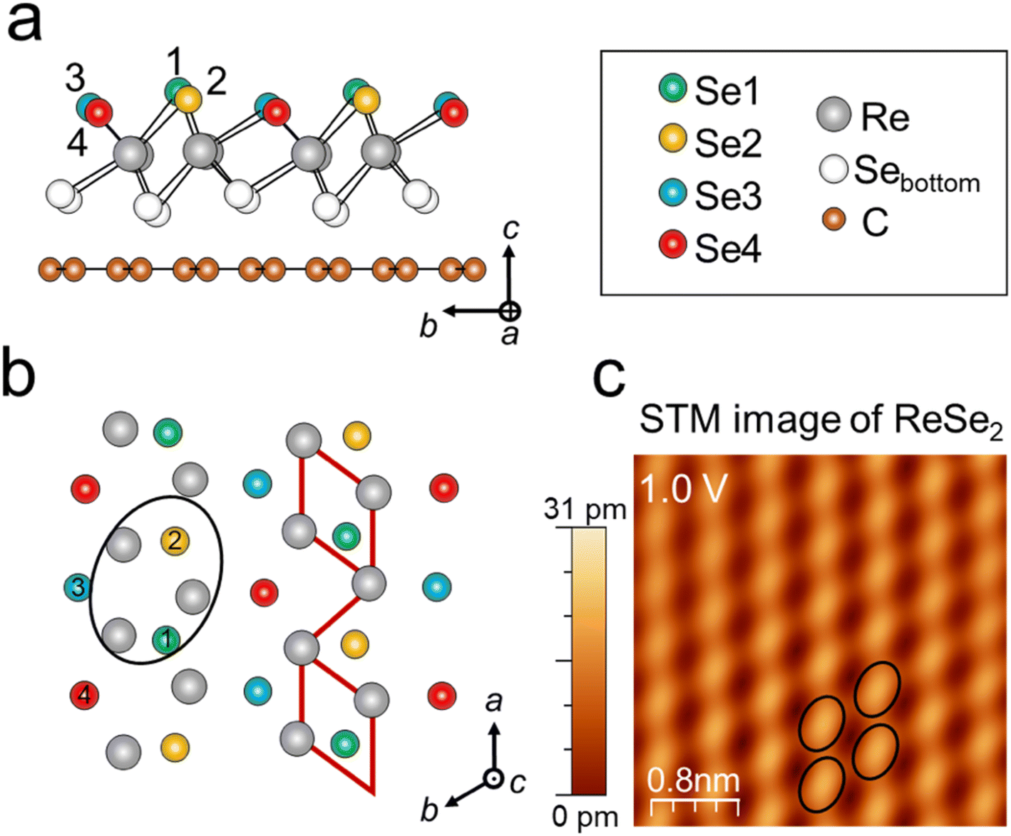 | ||
| Fig. 1 Monolayer (ML) ReSe2 on a graphene substrate. (a and b) The side- and top-view structures of ML ReSe2. The Se atoms in the topmost layer are classified into Se1 (green), Se2 (orange), Se3 (blue), and Se4 (red) based on their height along the c-axis. The Re-chain is indicated by red solid lines in (b). (c) The STM topography image of ReSe2 shows the oval feature with a lattice constant of ∼6.6 Å (It = 30 pA). | ||
Fig. 2a shows an STM topography of ReSe2 films grown on bilayer graphene (BLG). We could observe defect features on ReSe2 surfaces, which appear as local depression indicated by a box in Fig. 2b. Fig. 2c shows an atomistic image taken from the box area in Fig. 2b. In the defect region (black dashed circle), one oval spot (at the center of the dashed circle) shows a slightly suppressed contrast with a dark hole defect at its left side (marked by a red triangle). The marked hole defect is located at the Se4 site and identified as an Se4 vacancy. This observation is further corroborated by the DFT-simulated STM image of an Se4 vacancy (diamond-shaped inset of Fig. 2c). The simulated image accurately reproduces the hole-like feature and location of the observed Se4 vacancy in the STM image. Detail line profiles along the Se4 vacancy are provided in ESI Fig. S2.† More STM image examples of Se4 vacancies are also available in Fig. S3† (supported by first-principles DFT/HSE06 STM simulations in Fig. S4†). The formation energy of all Se vacancies is calculated in Fig. 2d, confirming that the Se4 vacancy observed via STM is indeed energetically favored (0.66 eV per vacancy). Our calculated results are in line with previous DFT calculations.31 Understanding how this intrinsic defect of Se4 vacancy influences the electronic properties of ML ReSe2 is important for potential applications. Therefore, direct experimental observations of the defect state of Se4 vacancy are essential for this purpose.
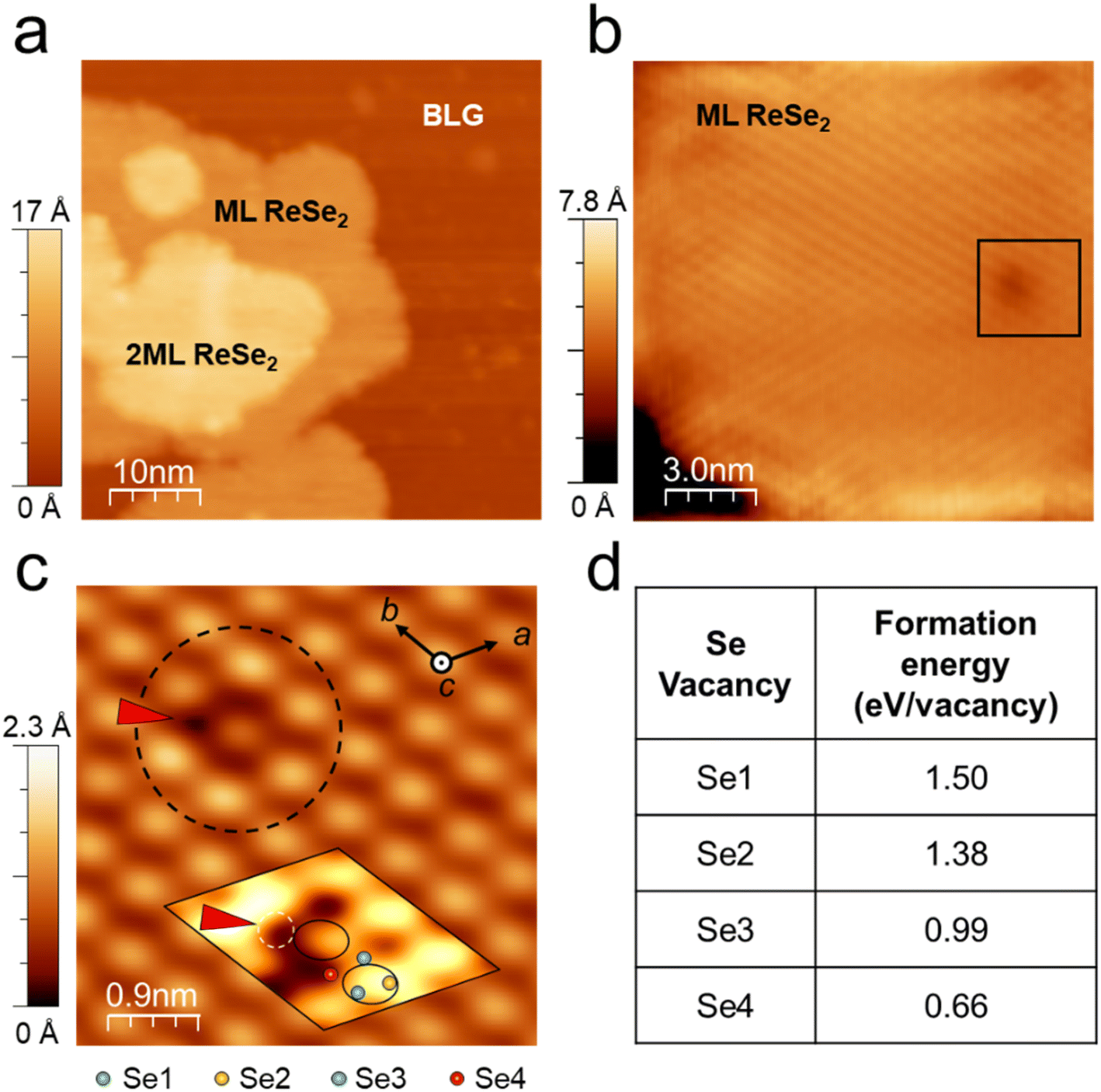 | ||
| Fig. 2 Se4 vacancy in ML ReSe2. (a) STM image of ReSe2 film grown on bilayer graphene (BLG) (Vb = 1.0 V, It = 30 pA). (b) STM image shows some defect feature with a suppressed contrast (marked by a black box) (Vb = 1.0 V, It = 30 pA). (c) Atomistic STM image of an Se4 vacancy. The Se4 vacancy is indicated by the red triangle inside the defect region (black dashed circle). The diamond-shaped inset in (c) is a HSE06 DFT simulation image of an Se4 vacancy. (d) Formation energy of all Se vacancies based on optB86b DFT total energy calculations. | ||
Fig. 3a shows dI/dV spectra measured at the Se4 defect site and the defect-free area in the inset image marked by red and black crosses, respectively. The dI/dV spectrum taken from the defect-free area (black curve) shows a bandgap of ∼1.7 eV with a valence band maximum (EVBM) ∼−1.2 eV and conduction band minimum (ECBM) ∼0.5 eV, which are in agreement with a previous report.44 In comparison, our HSE06-calculated bandgap of monolayer ReSe2 (1.83 eV) also agrees well to the experimental value of 1.7 eV and aligns with the reported HSE06 and G0W0 values of 1.62 eV (ref. 45) and 2.09 eV (ref. 5). On the other hand, at the Se4 vacancy, the dI/dV spectrum (red curve) reveals a defect state peak at around −1.0 V near EVBM (indicated by a red arrow).
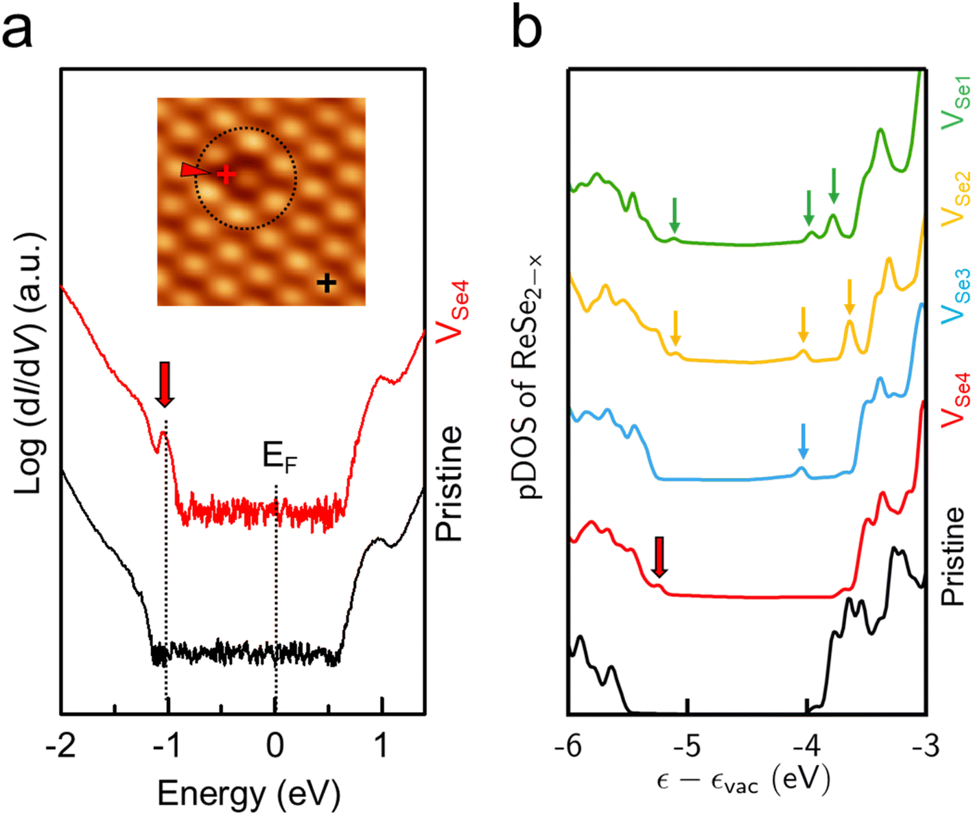 | ||
| Fig. 3 The defect state of the Se4 vacancy. (a) dI/dV spectra were measured at the Se4 defect site (red curve) and defect-free area (black curve). The inset shows an STM image where STS measurements were taken (color coded). The Se4 vacancy is indicated by the red triangle. (b) The partial density of states (pDOS) was calculated based on the DFT HSE06 functional for different upper Se vacancies and pristine ReSe2; the green, orange, blue, red, and black curves correspond to the pDOS of Se1, Se2, Se3 and Se4 vacancies and pristine ReSe2, respectively. | ||
To further examine Se vacancies and their electronic structures, the DFT calculated density of states (DOS) for all four kinds of Se vacancies (namely, VSe1, VSe2, VSe3, and VSe4; see Fig. 1) are presented in Fig. 3b. It is obvious that the valence and conduction band edges are significantly modified with these Se vacancies when compared to pristine ReSe2/graphene (black curve). Besides the thermodynamic considerations (where VSe4 has the lowest formation energy), only VSe4 presents a defect state near the valence band edge (red arrow in Fig. 3b) while VSe1,2 and VSe3 exhibit multiple in-gap states within the band gap and a defect state around the middle of band gap, respectively. From our DFT partial DOS calculations (see Fig. S5†), the defect state in VSe4 near the valence band edge is largely contributed from the occupied 5d states of the undercoordinated Re atom neighboring the VSe4 defect. For the in-gap states observed in the other Se vacancies, they correspond mainly to the unoccupied dangling bond 5d states of the neighboring undercoordinated Re atoms as seen in the partial DOS in Fig. S5.† Additionally, the HSE06 theoretical STM images presented in Fig. S6† conclusively exclude the stable O- and S-substituents at the VSe1 site (which was proposed in ref. 31) due to the mismatch in their STM topographical contrast. To aid the reader, the O- and S-substituted ReSe2 structures are provided in Fig. S7.† Referring to Fig. 3b for VSe4, an additional peak (denoted by a red arrow) is observed near the valence band edge, while the conduction band edge is virtually unaffected; this corroborates our experimental STS results (Fig. 3a). Thus, we conclude that the most likely Se vacancies found on our samples are due to VSe4. In passing, we would also like to highlight that the role of the graphene substrate acts as a conductive support to the ReSe2 layer (Fig. S8†). As reported in our previous work,35 graphene facilitates the donation of charges through the vdW gap and results in the so-called compressed/trapped charges within the vdW gap. This allows one to image the topologies of the graphene-donated in-gap states of ReSe2 as evidenced in ref. 35. In addition, in order to accurately describe the electronic structure of the heterostructure interface, one will need to go beyond DFT and utilize higher-level theories (e.g. using the GW approximation46,47) where the image charge screening may significantly renormalize the bandgap of the 2D material. This is currently beyond the scope of this work.
The spatially extended defect state of the Se4 vacancy is also directly observed in STM topographs. Fig. 4a and b present STM images of an Se4 vacancy taken at +1.0 V (conduction band region) and −1.0 V (defect state level), respectively. The defect area (marked by the dashed circle in Fig. 4b) reveals very bright protrusion at −1.0 V, while a deeply sunken region with a dark contrast appears at +1.0 V in the corresponding defect area (Fig. 4a).
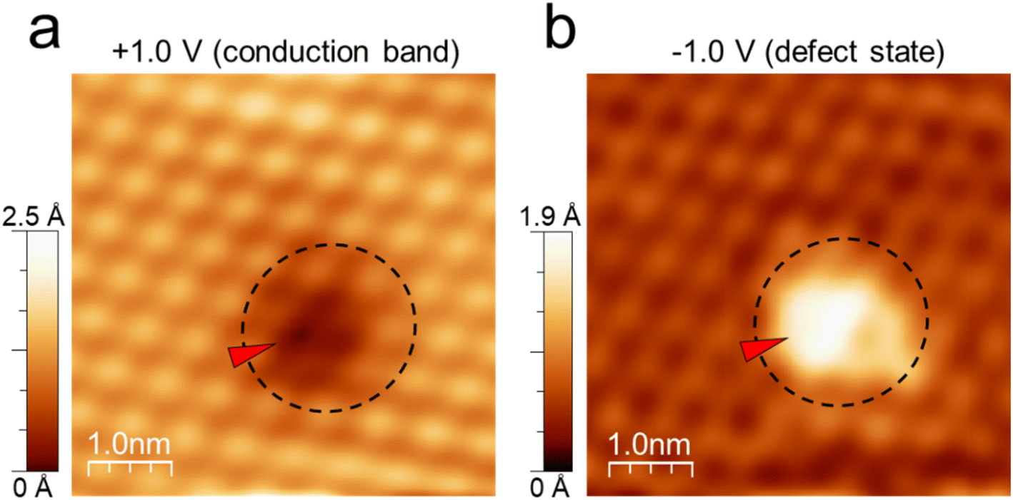 | ||
| Fig. 4 The spatially extended defect state of an Se4 vacancy. STM images of an Se4 vacancy at (a) +1.0 V (conduction band region) and (b) −1.0 V (defect state level). | ||
In essence, via a close collaboration between high-resolution STM/STS experiments and advanced DFT-based STM modeling (by including the DFT-parametrized linear combination of tip orbitals), we unambiguously provide a direct characterization of Se vacancies on the ReSe2 surface-elucidating both the actual atomic and electronic structures on an equal footing in this integrated STM approach. We advocate that such direct measurement and characterization of surface defects and their complexes are essential for providing a more complete picture of surface-dominated properties of important low-dimensional nanomaterials (as evidenced in our recent work of ultrathin complex oxides on copper surfaces41).
Conclusions
Microscopic investigation using STM/S is performed to understand the nature of Se vacancies in ML ReSe2 on a graphene substrate. Among four possible Se vacancy sites, a commonly observed defect is the Se4 vacancy, which is located close to the Re layer. Formation energy calculations support that the Se4 vacancy is thermodynamically favored, agreeing with STM observations. DFT calculations also indicate that with the Se4 vacancy, only the valence band edge is slightly up-shifted in energy, while the conduction band edge of ReSe2 is unperturbed. Our dI/dV spectroscopy results clearly show that the Se4 vacancy has a defect state at −1.0 V near EVBM (−1.2 V), which is in good agreement with the DFT prediction. The area near the Se4 vacancy exhibits bright protrusion in the STM topograph probed at −1.0 V (defect state level), spatially mapping the electronic state of the Se4 vacancy. Our results may have strong implications on how this type of ReSe2/graphene heterojunction (with naturally occurring Se vacancies) may behave in actual electronic device applications. By establishing a close collaboration between high-resolution STM/STS experiments and advanced STM models, we confidently elucidate both the actual atomic and electronic structures of low-dimensional materials.Author contributions
J. K. initiated the project. A. S. and J. K. coordinated the project. B. K. C. and Y. J. C. prepared the high-quality samples. The STM/STS measurements and data analysis were performed by N. H. L., T. T. L., K. J., and J. K. J.-H. K., G. L., and A. S. performed DFT calculations and theoretical analyses. N. H. L., J.-H. K., Y. J. C., A. S., and J. K. wrote the manuscript with contributions from all authors. All authors have discussed the results and commented on the manuscript.Conflicts of interest
There are no conflicts to declare.Acknowledgements
This work is supported by National Research Foundation (NRF) grants funded by the Korean government (NRF-2018R1D1A1B07050144, NRF-2019R1A6A1A11053838, NRF-2018M3D1A1058536, NRF-2020R1A2C200373211, NRF-2021R1A6A3A14040322). J. Kim acknowledges the support of an internal R&D programme at KAERI funded by the Ministry of Science and ICT (MIST) of the Republic of Korea (524420-23). Computational resources have been kindly provided by the KISTI Super-computing Center (KSC-2021-CRE-0450). This work was also supported by the 2022 Research Fund of the University of Seoul for Young Jun Chang.References
- Q. H. Wang, K. Kalantar-Zadeh, A. Kis, J. N. Coleman and M. S. Strano, Nat. Nanotechnol., 2012, 7, 699–712 CrossRef CAS PubMed.
- F. Xia, H. Wang, D. Xiao, M. Dubey and A. Ramasubramaniam, Nat. Photonics, 2014, 8, 899–907 CrossRef CAS.
- P. Ranjan, S. Gaur, H. Yadav, A. B. Urgunde, V. Singh, A. Patel, K. Vishwakarma, D. Kalirawana, R. Gupta and P. Kumar, Nano Convergence, 2022, 9, 26 CrossRef CAS PubMed.
- D. Wolverson, S. Crampin, A. S. Kazemi, A. Ilie and S. J. Bending, ACS Nano, 2014, 8, 11154–11164 CrossRef CAS PubMed.
- H. X. Zhong, S. Gao, J. J. Shi and L. Yang, Phys. Rev. B: Condens. Matter Mater. Phys., 2015, 92, 115438 CrossRef.
- A. Arora, J. Noky, M. Drüppel, B. Jariwala, T. Deilmann, R. Schneider, R. Schmidt, O. Del Pozo-Zamudio, T. Stiehm, A. Bhattacharya, P. Krüger, S. Michaelis de Vasconcellos, M. Rohlfing and R. Bratschitsch, Nano Lett., 2017, 17, 3202–3207 CrossRef CAS PubMed.
- S. Bae and S. Sim, J. Korean Phys. Soc., 2022, 81, 532–548 CrossRef CAS.
- K. Volckaert, B. K. Choi, H. J. Kim, D. Biswas, D. Puntel, S. Peli, F. Parmigiani, F. Cilento, Y. J. Chang and S. Ulstrup, Phys. Rev. Mater., 2023, 7, L041001 CrossRef CAS.
- Z. Qiu, M. Trushin, H. Fang, I. Verzhbitskiy, S. Gao, E. Laksono, M. Yang, P. Lyu, J. Li, J. Su, M. Telychko, K. Watanabe, T. Taniguchi, J. Wu, A. H. C. Neto, L. Yang, G. Eda, S. Adam and J. Lu, Sci. Adv., 2022, 5, eaaw2347 CrossRef PubMed.
- S. H. Yang, K. C. Lee, M. Y. Tsai, Y. M. Chang, C. Y. Lin, F. S. Yang, K. Watanabe, T. Taniguchi, C. H. Lien, C. H. Ho, M. Li, Y. F. Lin and Y. C. Lai, Nano Energy, 2019, 66, 104107 CrossRef CAS.
- J. Ahn, K. Ko, J. Kyhm, H. S. Ra, H. Bae, S. Hong, D. Y. Kim, J. Jang, T. W. Kim, S. Choi, J. H. Kang, N. Kwon, S. Park, B. K. Ju, T. C. Poon, M. C. Park, S. Im and D. K. Hwang, ACS Nano, 2021, 15, 17917–17925 CrossRef CAS PubMed.
- Z. Fang, B. Bueken, D. E. De Vos and R. A. Fischer, Angew. Chem., Int. Ed., 2015, 54, 7234–7254 CrossRef CAS PubMed.
- Z. Lin, A. McCreary, N. Briggs, S. Subramanian, K. Zhang, Y. Sun, X. Li, N. J. Borys, H. Yuan, S. K. Fullerton-Shirey, A. Chernikov, H. Zhao, S. McDonnell, A. M. Lindenberg, K. Xiao, B. J. LeRoy, M. Drndić, J. C. M. Hwang, J. Park, M. Chhowalla, R. E. Schaak, A. Javey, M. C. Hersam, J. Robinson and M. Terrones, 2D Mater., 2016, 3, 042001 CrossRef.
- D. Rhodes, S. H. Chae, R. Ribeiro-Palau and J. Hone, Nat. Mater., 2019, 18, 541–549 CrossRef CAS PubMed.
- C. Xie, D. Yan, W. Chen, Y. Zou, R. Chen, S. Zang, Y. Wang, X. Yao and S. Wang, Mater. Today, 2019, 31, 47–68 CrossRef CAS.
- Z. Yu, Y. Pan, Y. Shen, Z. Wang, Z. Y. Ong, T. Xu, R. Xin, L. Pan, B. Wang, L. Sun, J. Wang, G. Zhang, Y. W. Zhang, Y. Shi and X. Wang, Nat. Commun., 2014, 5, 5290 CrossRef CAS PubMed.
- Z. Wu, Z. Luo, Y. Shen, W. Zhao, W. Wang, H. Nan, X. Guo, L. Sun, X. Wang, Y. You and Z. Ni, Nano Res., 2016, 9, 3622–3631 CrossRef CAS.
- M. G. Stanford, P. R. Pudasaini, E. T. Gallmeier, N. Cross, L. Liang, A. Oyedele, G. Duscher, M. Mahjouri-Samani, K. Wang, K. Xiao, D. B. Geohegan, A. Belianinov, B. G. Sumpter and P. D. Rack, Adv. Funct. Mater., 2017, 27, 1702829 CrossRef.
- Z. Ding, Q. X. Pei, J. W. Jiang and Y. W. Zhang, J. Phys. Chem. C, 2015, 119, 16358–16365 CrossRef CAS.
- B. Peng, Z. Ning, H. Zhang, H. Shao, Y. Xu, G. Ni and H. Zhu, J. Phys. Chem. C, 2016, 120, 29324–29331 CrossRef CAS.
- M. Yarali, H. Brahmi, Z. Yan, X. Li, L. Xie, S. Chen, S. Kumar, M. Yoon, K. Xiao and A. Mavrokefalos, ACS Appl. Mater. Interfaces, 2018, 10, 4921–4928 CrossRef CAS PubMed.
- H. J. Kim, N. Van Quang, T. H. Nguyen, S. Kim, Y. Lee, I. H. Lee, S. Cho, M. J. Seong, K. Kim and Y. J. Chang, Nanoscale Res. Lett., 2022, 17, 26 CrossRef CAS PubMed.
- C. Tsai, H. Li, S. Park, J. Park, H. S. Han, J. K. Nørskov, X. Zheng and F. Abild-Pedersen, Nat. Commun., 2017, 8, 15113 CrossRef PubMed.
- J. Yang, Y. Wang, M. J. Lagos, V. Manichev, R. Fullon, X. Song, D. Voiry, S. Chakraborty, W. Zhang, P. E. Batson, L. Feldman, T. Gustafsson and M. Chhowalla, ACS Nano, 2019, 13, 9958–9964 CrossRef CAS PubMed.
- X. Wang, Y. Zhang, H. Si, Q. Zhang, J. Wu, L. Gao, X. Wei, Y. Sun, Q. Liao, Z. Zhang, K. Ammarah, L. Gu, Z. Kang and Y. Zhang, J. Am. Chem. Soc., 2020, 142, 4298–4308 CrossRef CAS PubMed.
- X. Yan, L. Zhuang, Z. Zhu and X. Yao, Nanoscale, 2021, 13, 3327–3345 RSC.
- M. Kianinia, Z. Q. Xu, M. Toth and I. Aharonovich, Appl. Phys. Rev., 2022, 9, 011306 CAS.
- H. Nan, Z. Wang, W. Wang, Z. Liang, Y. Lu, Q. Chen, D. He, P. Tan, F. Miao, X. Wang, J. Wang and Z. Ni, ACS Nano, 2014, 8, 5738–5745 CrossRef CAS PubMed.
- P. K. Chow, R. B. Jacobs-Gedrim, J. Gao, T. M. Lu, B. Yu, H. Terrones and N. Koratkar, ACS Nano, 2015, 9, 1520–1527 CrossRef CAS PubMed.
- Z. Wu, W. Zhao, J. Jiang, T. Zheng, Y. You, J. Lu and Z. Ni, J. Phys. Chem. C, 2017, 121, 12294–12299 CrossRef CAS.
- Y. Zhu, L. Tao, X. Chen, Y. Ma, S. Ning, J. Zhou, X. Zhao, M. Bosman, Z. Liu, S. Du, S. T. Pantelides and W. Zhou, iScience, 2021, 24, 103456 CrossRef CAS PubMed.
- J. Kim, H. Nam, S. Qin, S. Kim, A. Schroeder, D. Eom and C. K. Shih, Rev. Sci. Instrum., 2015, 86, 093707 CrossRef PubMed.
- G. Kresse and J. Hafner, Phys. Rev. B: Condens. Matter Mater. Phys., 1993, 47, 558–561 CrossRef CAS PubMed.
- G. Kresse and J. Hafner, Phys. Rev. B: Condens. Matter Mater. Phys., 1994, 49, 14251–14269 CrossRef CAS PubMed.
- T. Thi Ly, Y. J. Lee, B. Ki Choi, H. Lee, H. Jin Kim, G. Duvjir, N. Huu Lam, K. Jang, K. Palotás, Y. Jun Chang, A. Soon and J. Kim, Appl. Surf. Sci., 2022, 579, 152187 CrossRef CAS.
- J. Klimeš, D. R. Bowler and A. Michaelides, J. Phys.: Condens.Matter, 2010, 22, 022201 CrossRef PubMed.
- J. Heyd, G. E. Scuseria and M. Ernzerhof, J. Chem. Phys., 2003, 118, 8207–8215 CrossRef CAS.
- J. Heyd, G. E. Scuseria and M. Ernzerhof, J. Chem. Phys., 2006, 124, 219906 CrossRef.
- K. Palotás and W. A. Hofer, J. Phys.: Condens.Matter, 2005, 17, 2705–2713 CrossRef.
- G. Mándi and K. Palotás, Phys. Rev. B: Condens. Matter Mater. Phys., 2015, 91, 165406 CrossRef.
- Y. J. Lee, T. T. Ly, T. Lee, K. Palotás, S. Y. Jeong, J. Kim and A. Soon, Appl. Surf. Sci., 2021, 562, 150148 CrossRef CAS.
- B. A. Parkinson, J. Ren and M. H. Whangbo, J. Am. Chem. Soc., 1991, 113, 7833–7837 CrossRef CAS.
- H. J. Lamfers, A. Meetsma, G. A. Wiegers and J. L. de Boer, J. Alloys Compd., 1996, 241, 34–39 CrossRef CAS.
- B. K. Choi, S. Ulstrup, S. M. Gunasekera, J. Kim, S. Y. Lim, L. Moreschini, J. S. Oh, S. H. Chun, C. Jozwiak, A. Bostwick, E. Rotenberg, H. Cheong, I. W. Lyo, M. Mucha-Kruczynski and Y. J. Chang, ACS Nano, 2020, 14, 7880–7891 CrossRef CAS PubMed.
- S. Haastrup, M. Strange, M. Pandey, T. Deilmann, P. S. Schmidt, N. F. Hinsche, M. N. Gjerding, D. Torelli, P. M. Larsen, A. C. Riis-Jensen, J. Gath, K. W. Jacobsen, J. Jørgen Mortensen, T. Olsen and K. S. Thygesen, 2D Mater., 2018, 5, 042002 CrossRef CAS.
- M. M. Ugeda, A. J. Bradley, S. F. Shi, F. H. da Jornada, Y. Zhang, D. Y. Qiu, W. Ruan, S. K. Mo, Z. Hussain, Z. X. Shen, F. Wang, S. G. Louie and M. F. Crommie, Nat. Mater., 2014, 13, 1091–1095 CrossRef CAS PubMed.
- A. C. Riis-Jensen, J. Lu and K. S. Thygesen, Phys. Rev. B, 2020, 101, 121110 CrossRef CAS.
Footnotes |
| † Electronic supplementary information (ESI) available. See DOI: https://doi.org/10.1039/d3na00363a |
| ‡ These authors contributed equally to this work. |
| This journal is © The Royal Society of Chemistry 2023 |