
 Open Access Article
 This Open Access Article is licensed under a
 Creative Commons Attribution 3.0 Unported Licence
Consolidation and performance gains in plasma-sintered printed nanoelectrodes†
Lukas F.
Engel
 a,
Lola
González-García
*ab and
Tobias
Kraus
*ac
a,
Lola
González-García
*ab and
Tobias
Kraus
*ac
aINM – Leibniz Institute for New Materials, Campus D2 2, 66123 Saarbrücken, Germany. E-mail: lola.gonzalez-garcia@leibniz-inm.de; Tel: +49 (0)681-9300-269
bDepartment of Materials Science and Engineering, Saarland University, Campus D2 2, 66123 Saarbrücken, Germany
cColloid and Interface Chemistry, Saarland University, Campus D2 2, 66123 Saarbrücken, Germany. E-mail: tobias.kraus@leibniz-inm.de; Tel: +49 (0)681-9300-389
First published on 11th July 2023
Abstract
We report on the unusual, advantageous ageing of flexible transparent electrodes (FTEs) that were self-assembled from oleylamine-capped gold nanospheres (AuNPs) by direct nanoimprinting of inks with different particle concentrations (cAu = 3 mg mL−1 to 30 mg mL−1). The resulting lines were less than 2.5 μm wide and consisted of disordered particle assemblies. Small-Angle X-ray Scattering confirmed that particle packing did not change with ink concentration. Plasma sintering converted the printed structures into lines with a thin, electrically conductive metal shell and a less conductive hybrid core. We studied the opto-electronic performance directly after plasma sintering and after fourteen days of storage at 22 °C and 55% rH in the dark. The mean optical transmittance ![[T with combining macron]](https://www.rsc.org/images/entities/i_char_0054_0304.gif) 400–800 in the range from 400 nm to 800 nm increased by up to ≈ 3%, while the sheet resistance Rsh strongly decreased by up to ≈ 82% at all concentrations. We correlated the changes with morphological changes visible in scanning and transmission electron microscopy and identified two sequential ageing stages: (I) post-plasma relaxation effects in and consolidation of the shell, and (II) particle re-organization, de-mixing, coarsening, and densification of the core with plating of Au from the core onto the shell, followed by solid-state de-wetting (ink concentrations cAu < 15 mg mL−1) or stability (cAu ≥ 15 mg mL−1). The plating of Au from the hybrid core improved the FTEs' Figure of Merit FOM = 400–800·Rsh−1 by up to ≈ 5.8 times and explains the stable value of ≈ 3.3%·Ωsq−1 reached after 7 days of ageing at cAu = 30 mg mL−1.
400–800 in the range from 400 nm to 800 nm increased by up to ≈ 3%, while the sheet resistance Rsh strongly decreased by up to ≈ 82% at all concentrations. We correlated the changes with morphological changes visible in scanning and transmission electron microscopy and identified two sequential ageing stages: (I) post-plasma relaxation effects in and consolidation of the shell, and (II) particle re-organization, de-mixing, coarsening, and densification of the core with plating of Au from the core onto the shell, followed by solid-state de-wetting (ink concentrations cAu < 15 mg mL−1) or stability (cAu ≥ 15 mg mL−1). The plating of Au from the hybrid core improved the FTEs' Figure of Merit FOM = 400–800·Rsh−1 by up to ≈ 5.8 times and explains the stable value of ≈ 3.3%·Ωsq−1 reached after 7 days of ageing at cAu = 30 mg mL−1.
1. Introduction
Flexible and transparent electrodes (FTEs) are indispensable components of modern opto-electronics such as foldable smartphones or wearables.1 Metal grids with (sub-)micron line widths allow to combine mechanical flexibility and optical transparency with electrical conductance.2 Micron-scale conductive metal lines are sufficiently conductive for many applications at areal fractions that let most light pass through. A useful figure of merit of such an electrode is the ratio between optical transmittance and sheet resistance.3 It can be tailored to the application by varying the grid pattern, line dimensions, or metal type, for example.4Direct nanoimprinting of colloidal metal inks is an established route to metal grid FTEs.5 Printing is feasible in a single, roll-to-roll-compatible step under ambient conditions.6 It is possible to print at the sub-micron resolution required for ultra-high definition displays.7 Advanced printing processes use a patterned polydimethylsiloxane (PDMS) elastomer stamp that patterns a colloidal metal ink when it meets the substrate. The stamp absorbs the solvent and/or its vapors, the colloids concentrate and self-assemble inside the stamp's cavities, and percolating networks form that follow the stamp's features.8
Ko et al.9 and Park et al.10 used such a process and nanoimprinted Au nanospheres with a core diameter of dc ≈ 1 nm to 3 nm and strongly bound hexanethiol ligands, dispersed in α-terpineol. Kister et al.7 employed Au nanospheres with dc ≈ 3.2 nm and weakly bound dodecylamine (C12) ligands, dispersed in cyclohexane. Maurer et al.8 imprinted ultra-thin Au nanowires with dc ≈ 1.6 nm, lengths above 1.6 μm, and a weakly bound oleylamine (OAm, C18) ligand shell, dispersed in cyclohexane. Park et al.11 worked with Ag nanospheres with a core diameter of dc ≈ 3 nm to 7 nm and dodecylamine (C12) ligands, dispersed in a mixture of toluene and α-terpineol. Agrawal and Garnett12 used Ag nanocubes with a core edge length of ≈75 nm and a polyvinylpyrrolidone (PVP) ligand shell, dispersed in ethanol, to form monocrystalline structures.13
Nanoimprinting is usually followed by a densification step. For example, colloidal metal typically contains electrically insulating ligands that have to be removed after imprinting.14 Thermal, photonic, or plasma-based processes are commonly used for ligand removal and sintering.15 Nanoscale colloids can be plasma-sintered at temperatures far below the melting point of the bulk metal.16 Plasma sintering avoids softening of the polymer substrate, e.g. polyethylene terephthalate (PET) with Tg ≈ 75 °C.17 Oxygen-containing plasma removes organic ligands primarily through oxidation, while inert plasma acts by sputtering.18 Both accelerate surface diffusion on metals and cause sintering.19 Shaw et al.20 showed that low-pressure O2 plasma penetrates 440 nm thick layers of ceramic nanospheres (ZrO2, core diameter dc ≈ 3.7 nm, trioctylphosphine oxide ligand shell) and removes virtually all organics while retaining the individual nanospheres. Reinhold et al.21 and Ma et al.22 provided evidence for the formation of a conductive Ag shell around an insulating core in a low-pressure Ar plasma for films of printed and drop-casted Ag nanospheres (e.g., dc ≈ 23 nm with a gum arabicum ligand shell). Engel et al.23 reported the formation of a conductive gold shell on top of an oleylamine-gold core for nanoimprinted lines of ultra-thin Au nanowires (AuNWs, dc ≈ 1.7 nm) or of Au nanospheres (AuNPs, dc ≈ 3.7 nm) in a low-pressure H2/Ar plasma.
The last three reports find a strongly improved conductance immediately after plasma treatment. Few authors report on the stability of this improvement or on the efficiency of metal use. It is known that thermally annealed random networks of Ag nanowires degrade as a function of temperature, humidity, light, and electric current.24–29 Such electrodes may fragment into spheres upon heating due to the Rayleigh–Plateau instability30 and are prone to failure due to electromigration. They are susceptible to UV light and chemical corrosion (sulfides, oxygen, and acids), which can be prevented by protective coatings that reduce surface diffusivity and the Rayleigh–Plateau instability. Maurer et al.31,32 reported that dip-coated layers (up to 10 nm thick) of AuNWs on glass substrate degraded within hours at room temperature, unless they were coarsened by a H2/Ar plasma. Annealing resulted in de-wetting, which accelerated with growing temperature and decreasing film thickness. Engel et al.33 examined the stability of grid-like FTEs (up to ≈ 275 nm thick) imprinted from AuNWs at different Au concentrations cAu on PET foil and identified ageing by solid-state de-wetting of the shell, de-mixing of the hybrid core, and collapse of the shell. All reports indicated a degradation with time that has to be prevented via additional coatings or other stabilizing measures.
Here, we show that the degradation of plasma-treated metal grid FTEs is connected to the porosity of the conductive shell and the residual organics inside their hybrid core. We printed FTEs using gold nanospheres (AuNPs) at different concentrations to obtain parallel lines. Their structures were analyzed via Small-Angle X-ray Scattering (SAXS) and the lines were sintered in a H2/Ar plasma. Electron microscopy (SEM/TEM) before and after sintering indicated the formation of increasingly smooth lines with growing gold concentration. The mean optical transmittances (400–800) increased by up to ≈ 3.17% within 14 days after sintering, while the electrical resistance Rsh strongly decreased by up to ≈ 82.2%, depending on the particle concentration. Detailed analyses of the morphological changes indicated that compact, stable shells formed during plasma sintering. They covered hybrid cores that de-mixed after sintering such that additional metal was plated onto the shell, increasing conductance.
2. Materials and methods
2.1. Synthesis of Au nanospheres
2.2. Small-angle X-ray scattering (SAXS)
The AuNP core size dsp and the colloidal state of order in the dispersions were determined via SAXS. The respective dispersion was filled into a glass mark-tube from Hilgenberg GmbH (Malfeld, Germany) with an inner diameter of 1.5 mm. The tube was sealed with a fast-curing two-component epoxy from R&G Faserverbundwerkstoffe GmbH (Waldenbuch, Germany) to exclude solvent evaporation. Each sample was measured for a total of 30 min. The solvent's background was accounted for by measuring its scattering curve separately and subtracting it from the sample curves. To determine dsp, fitting was performed using the software SASfit from the Laboratory for Neutron Scattering at Paul Scherrer Institute (Villigen, Switzerland).The spheres' structural arrangement within the pre-plasma lines was studied in transmission right after imprinting on PET. Measurements were performed at room temperature on ambient air to prevent any influence from drawing vacuum. Each sample was measured for 120 min in total.
The scattering setup consisted of a Xeuss 2.0 HR SAXS/WAXS instrument from Xenocs SAS (Grenoble, France) with a Cu Kα source and a detector PILATUS3 R 1 M from DECTRIS AG (Baden, Switzerland) which was placed at a distance of about 550 mm from the samples. Precise calibration of this distance was ensured using a standard of Ag behenate before each measurement. Through azimuthal integration, the scattering curves were obtained from the two-dimensional scattering images using the software Foxtrot from Synchrotron SOLEIL (Saint-Aubin, France).
2.3. Thermogravimetric analysis (TGA)
The sample for TGA was prepared by drying 0.360 mL of a 20 mg mL−1 AuNP dispersion in a crucible made from aluminum oxide. To remove any solvent and moisture, the sample was dried in a drying oven for 16 h at 30 °C and 50 mbar before being placed in an analyzer of type STA 449 F3 Jupiter from NETZSCH-Gerätebau GmbH (Selb, Germany). The sample was heated from room temperature to 1200 °C at a rate of 10 °C min−1 in synthetic dry air while the mass was continuously recorded from 50 °C onward.2.4. Nanoimprinting
Both masters had to be silanized prior to the moulding procedure. Silanization of the silicon master was carried out without pre-treatment, while silanization of the PDMS master was performed after its plasma activation for 1.5 min using an oxygen plasma at 0.3 mbar in a low pressure plasma reactor of type Pico from Diener electronic GmbH & Co. KG (Ebhausen, Germany). Each silanization was performed inside a conventional glass desiccator with a snap-on vial cap containing 30 μL of (tridecafluoro-1,1,2,2-tetrahydrooctyl)trichlorosilane from abcr GmbH (Karlsruhe, Germany). The snap-on vial cap was shielded from the respective master to achieve uniform silanization. Firstly, the desiccator was flushed with Ar (the silane is sensitive to humidity), evacuated to 3 mbar, and disconnected from the vacuum pump. After 30 min at room temperature, the desiccator was slowly ventilated with air.
The pre-polymer and the cross-linker of a PDMS kit, Sylgard 184 from Dow Inc. (Midland, USA), were mixed in a 10![[thin space (1/6-em)]](https://www.rsc.org/images/entities/char_2009.gif) :1 (w/w) ratio prior to degassing in a Speedmixer DAC 600.2 VAC-P from Hauschild GmbH & Co. KG (Hamm, Germany) at 2350 rpm and 1 mbar for 3 min. The resulting mixture was poured onto the respective master which carried a Teflon ring (2 mm thick) as spacer, sealed at the edges with add-i-gum light N from DE Healthcare Products (Gillingham, UK), and a glass plate as top sealing to ensure uniform thickness. The PDMS was cured for 3 h at 80 °C before carefully peeling off the replica along the stamp channels.
:1 (w/w) ratio prior to degassing in a Speedmixer DAC 600.2 VAC-P from Hauschild GmbH & Co. KG (Hamm, Germany) at 2350 rpm and 1 mbar for 3 min. The resulting mixture was poured onto the respective master which carried a Teflon ring (2 mm thick) as spacer, sealed at the edges with add-i-gum light N from DE Healthcare Products (Gillingham, UK), and a glass plate as top sealing to ensure uniform thickness. The PDMS was cured for 3 h at 80 °C before carefully peeling off the replica along the stamp channels.
The replica of the PDMS master was cut into two equal halves, each being an imprinting stamp with an area of 3.5 cm × 8 cm of which 3.5 cm × 7 cm were patterned and 3.5 cm × 0.5 cm at either end were not. The latter served as run-in and run-out areas during imprinting. Larger areas can be printed using the complete replicate.8
2.5. Plasma sintering
Plasma sintering was performed within a low pressure 13.56 MHz RF plasma reactor of type Pico from Diener electronic GmbH & Co. KG (Ebhausen, Germany) right after nanoimprinting. A mixture of 5% H2 in 95% Ar (H2/Ar) served as process gas. Plasma sintering was carried out at room temperature for 20 min at ≈ 0.3 mbar with 100 W RF power.2.6. Sheet resistance measurements
The electrodes' sheet resistances Rsh were determined in 2-point-probe configuration with a multi-channel multi-meter (DAQ6510 data acquisition logging multi-meter system) which was equipped with multiplexer cards (7702 40-channel differential multiplexer module with screw terminals) from Keithley Instruments GmbH (Germering, Germany). A fast drying Ag paste ACHESON Ag DAG 1415 from Plano GmbH (Wetzlar, Germany) and AGF 1 miniature crocodile clamps from SKS Kontakttechnik GmbH (Niederdorf, Germany) were used for contacting. The Ag paste was deposited as two parallel lines, each 1.5 cm long and spaced 1.5 cm apart, forming a square measurement field. The measured resistances corresponded directly to the desired sheet resistances. Measurements were automatically recorded every 10 min during storage under ambient conditions (T ≈ 22 °C, rH ≈ 55%) in the dark to avoid e.g. radiation heating.2.7. UV-vis spectroscopy
The electrodes' optical transmittances were determined using a Cary 5000 UV-vis-NIR spectrophotometer from Agilent Technologies Deutschland GmbH (Waldbronn, Germany) having a tungsten halogen light source for the visible and a deuterium arc light source for the UV range. The respective electrode on PET was mounted behind a blackened metal mask with circular aperture (5 mm in diameter). Measurements were carried out in the range 400 nm to 800 nm in double-beam mode against air at scan rates of 600 nm min−1. A PET substrate with the imprinted electrode on top was placed such that the blank side was in contact with the mask to prevent any damage to the electrode on the other side. Baselines of the bare PET substrates were recorded, too, as references.2.8. Cross-sectioning via focused ion beam (FIB)
Cross-sections of printed and of sintered lines were prepared with a FEI Versa 3D DualBeam from Thermo Fisher Scientific GmbH (Schwerte, Germany). The surfaces of the lines were protected by layers of Pt which were first deposited using the electron beam, and then with an ion beam.2.9. Transmission electron microscopy (TEM)
All FIB cuts were characterized at an acceleration voltage of 200 kV in a JEM 2010 from JEOL GmbH (Freising, Germany).2.10. Scanning electron microscopy (SEM)
For SEM imaging, either a FEI Quanta 400 ESEM or a FEI Versa 3D DualBeam from Thermo Fisher Scientific GmbH (Schwerte, Germany) with secondary electron detectors was used. Instead of PET, polished p-type silicon wafers from Siegert Wafer GmbH (Aachen, Germany) were used as substrate for better imaging.3. Results and discussion
Fig. 1 illustrates the performance of freshly prepared (purple) and aged (orange) metal-grid FTEs printed using inks with different gold concentrations cAu (denoted in the figure with the color gradient, where the intensity of the color indicates higher concentrations). We printed grids from oleylamine-capped gold nanospheres (AuNPs), plasma-sintered them, and compared their mean transmittances400–800 in the visible range to their sheet resistances Rsh immediately after plasma sintering and two weeks later. Sheet resistances Rsh and optical transmittances 400–800 consistently decreased with increasing concentration cAu in the range of 3–30 mg mL−1. Lower concentrations were insufficient to form percolating, conductive lines; higher concentrations led to optical transmittances of below 85%. The figure of merit according to Fraser and Cook,3| FOM = 400–800·Rsh−1, | (1) |
400–800 and Rsh at different concentrations cAu; it increased with cAu.
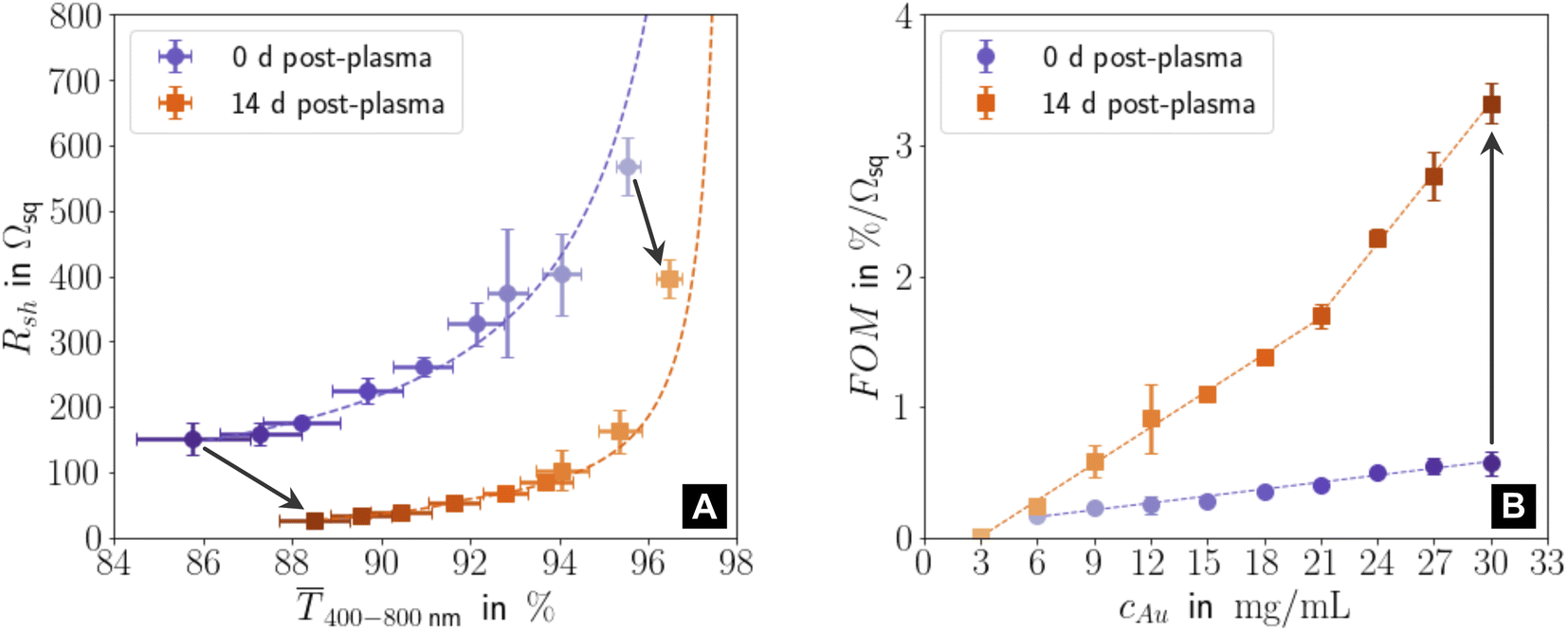 | ||
| Fig. 1 (A) Sheet resistances Rsh and mean optical transmittances 400–800 for electrodes directly after plasma sintering and fourteen days later. (B) Change of the figure of merit FOM = 400–800·Rsh−1 with gold concentration cAu for new and aged samples. All graphs show averages and standard deviations from three samples, and the corresponding fits (dashed lines). Fig. S1 in the ESI† has the complete data set and the fitting details for (A). Light colours represent lower cAu. | ||
Resistances were more sensitive to cAu than transmittances, and the FOM of aged electrodes was more sensitive to cAu than that of freshly sintered ones. During 14 days of ageing, 400–800 (Fig. S3 and S4 in the ESI† show the averaged optical transmittance spectra for all concentrations immediately after plasma sintering and 14 days later) always increased (by up to ≈ 3.17%) while Rsh always dropped (by up to ≈ 82.2%), which increased the FOM up to ≈ 5.8 times. This is in stark contrast to the situation for metal grid FTEs printed with oleylamine-capped ultra-thin gold nanowires (AuNWs). Their sheet resistances increased by ≈30% in 14 days for concentrations up to 3 mg mL−1, and they became non-conductive within 8 h for cAu ≥ 5 mg mL−1.33
We studied the ageing mechanisms to optimize the stability and performance of the affected FTEs. In the following, we give an overview of the resistances' temporal evolution, compare it to structural analyses, and develop mechanistic hypotheses.
The relative change in sheet resistance (Rsh,t − Rsh,t0)·Rsh,t0−1 = ΔRsh,t·Rsh,t0−1 at time t progressed in two sequential stages. Their exact progressions depended on cAu, but the qualitative features were similar for all concentrations. Differences between the stages were particularly distinct for cAu = 30 mg mL−1, the case shown in Fig. 2. An initial exponential decay (stage I) was followed by a reversed S-curve (stage II). We analyzed the morphological evolution of the lines and correlated it with the change in their resistance (Fig. 3).
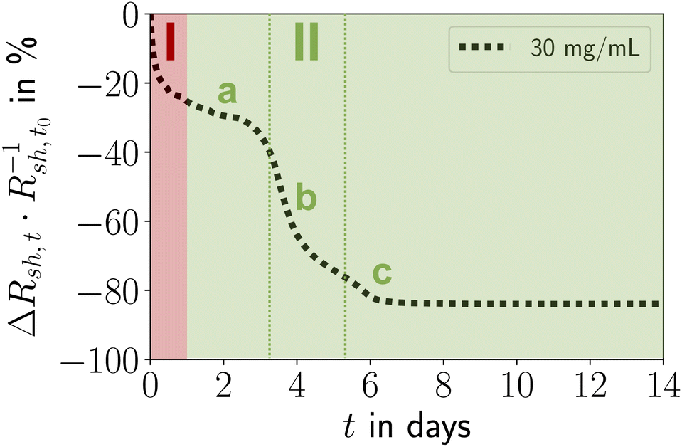 | ||
| Fig. 2 Stages I and II of electrode ageing: (I) post-plasma relaxation effects in and consolidation of the shell, (II) particle re-organization, de-mixing, coarsening, and densification of the core with Au plating onto the shell, followed by stabilization or (for cAu < 15 mg mL−1) solid-state de-wetting. Stage II can be split into an initial phase a, an intermediate phase b, and a final phase c. | ||
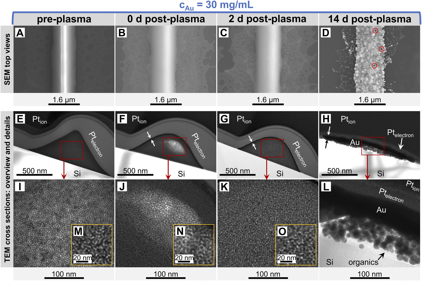 | ||
| Fig. 3 Surfaces and cross-sections of lines imprinted at 30 mg mL−1 before (A, E, I, M), immediately after (B, F, J, N), two days after (C, G, K, O), and fourteen days after (D, H, L) plasma sintering. They show the smooth line surface flanked by a thin layer of bleeded spheres (A) and the amorphous sphere arrangement in triangular shape (E, I and M) before, the now Gaussian-shaped core–shell structure (F, J and N) right after and (G, K and O) two days after as well as the densified core (H and L), the coarsened surface with occasional pores (red circles) and the coalesced bled spheres (D) fourteen days after plasma sintering. Note that each TEM image was taken from an individual TEM lamella. We prepared lamellae from different locations of the same FTE sample. | ||
The printed structure initially consisted of randomly and densely packed nanospheres. Small-angle X-ray scattering (SAXS, Fig. S6 of the ESI†) confirmed that the printed particles with a core diameter of dsp = 3.7 ± 0.37 nm packed with a center-to-center distance of ac–c = 5.61 ± 0.07 nm (Sections 3.1 and 3.2 in the ESI†). The surface-to-surface distance of the Au cores of as–s ≈ 1.91 nm was about the length of an oleylamine (OAm) molecule (lOAm ≈ 2.05 nm (ref. 36)), probably due to interdigitation of the OAm shells.37
The printed lines were slightly narrower than the stamp feature wc = 1.6 μm and had triangular cross-sections with a central ridge that appears as a bright center (Fig. 3A). Limited bleeding formed a sub-mono AuNP layer barely visible in the cross-section of Fig. 3E.
Plasma sintering blunted the ridge (Fig. 3B), reduced its height, and formed a conductive line with a Gaussian profile (Fig. 3F). Gold and OAm were moved or removed during plasma sintering. The outermost particles were sintered and formed a thin Au shell with a thickness of tshell = 8.07 ± 1.36 nm.23 This shell was slightly thicker than that reported for plasma-sintered AuNW lines.23
Ageing stage I (Fig. 2) was not accompanied by visible morphological changes (Fig. 3M–O). The resistance in Fig. 2 indicates that ageing started immediately after plasma sintering, but there were no changes visible in electron microscopy (EM) that would explain the initial drop in Rsh during stage I. The unchanged microstructure and the time scale suggest that stage I is dominated by stress relaxation that reduces atomic lattice distortions in the metal shell.38 Slow consolidation processes likely close small pores in the shell, and metal grain sizes increase. The overall process can be likened to the final stage of ceramic solid-phase sintering.39 It is interesting to compare it to the ageing of AuNW grids at high cAu. These rapidly age and degrade after plasma sintering by fast de-mixing and compaction of the hybrid core, processes that damage the conductive shell and are clearly visible in EM.33 We find that plasma-sintered spherical nanoparticles form a thicker,23 less porous shell that shields the hybrid core from the plasma. This limits the removal of OAm and fragments thereof from the core that dominates the ageing of AuNW-derived structures.33
Ageing stage II was characterized by a reversed S-curve course that can be divided (Fig. 2) into an initial, an intermediate, and a final phase. The decrease of Rsh started slowly, accelerated, and finally stabilized. This may be compared to powder sintering with a liquid phase due to a low-melting secondary powder component, where most of the densification occurs quickly in the intermediate phase, too.39 A similar liquid phase may form in the hybrid core due to ”melting” of the ligand shells that are partially degraded by plasma sintering.
The decrease of resistance in stage II suggests coordinated particle movement inside the core rather than the motion of single particles that fill gaps. This is consistent with the average particle spacing from SAXS as–s that is ≈48% below the particle diameter dsp and would not allow single particles to move inside packing. Instead, collective particle motion caused morphological changes that were clearly visible in electron microscopy Fig. 3D, H and L. The hybrid core had densified significantly, confirming the removal of a relevant fraction of OAm during plasma sintering. The surface of the lines had visibly coarsened after 14 days and pores were visible (indicated by red circles). We found that these pores appeared in lines printed at the same ink concentrations at similar densities, with spacings of at least 1 μm. This may indicate a “depletion” volume that forms below the pores. Metallic Au apparently migrated to the shell and increased its thickness from tshell = 8.07 ± 1.36 nm (ref. 23) up to ≈ 100 nm (Fig. 3H and L). This migration probably decreased Rsh and stabilized the aged lines against solid-state dewetting.40 The shell thickness was surprisingly uniform across the entire width, indicating uniform plating from the core onto the inside of the shell. The aged lines appeared slightly wider than before, probably because the core partially collapsed in height with an intact shell. This reduced optical transmittance, an effect overcompensated by coalescence of the spheres in the thin layers surrounding the lines (Fig. 3D). This coalescence reduced optical scattering and probably explains the 3.17% increase in optical transmittance. Larger Au spheres formed in the core, probably by Ostwald ripening.41
The ageing of lines printed at lower cAu was qualitatively similar (Fig. 4A–C). At cAu = 6 mg mL−1 to 12 mg mL−1 (Fig. 4A), stage I was unchanged, but the intermediate phase of stage II started earlier than at cAu = 30 mg mL−1 and caused a smaller relative decrease in Rsh.
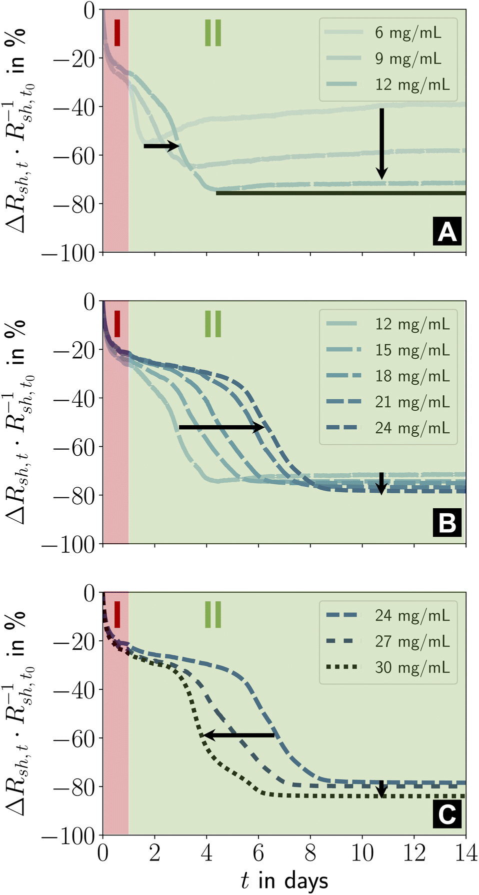 | ||
| Fig. 4 (A–C) Effect of ink concentration cAu on the two ageing stages I and II. Relative changes in sheet resistance during fourteen days of storage under ambient conditions in the dark are shown. The different concentrations were distributed over three plots for improved readability. Figure S2 in the ESI† illustrates the repeatability and the result for cAu = 3 mg mL−1. | ||
Previous studies reported that lines printed at low cAu were up to ≈ 41% wider, lower in height, more porous, and had disconnected gold parts that did not contribute to conductance.23 Lines printed at higher cAu had smoother surfaces and were higher and narrower (minimum width at cAu = 12 mg mL−1, Fig. 4B). Our recent results suggest that porous, flat, wide lines age unfavorably. The conductance decrease in stage II at cAu = 6 mg mL−1 strongly reminds of the ageing of wire-based electrodes33 imprinted at low concentrations that have a rough, porous surface and slowly degrade due to solid-state de-wetting.40
Lines printed at cAu = 12 mg mL−1 to 24 mg mL−1 (Fig. 4B) aged in similar ways. Stage II lasted longer with increasing cAu. The (stable) resistance in its final phase consistently decreased with increasing cAu, while its relative change increased due to the growing Au fraction in the hybrid core. The initial steep drop in relative Rsh remained unchanged, consistent with a relaxation mechanism. It is conceivable that the thin and wide lines that form at cAu ≤ 9 mg mL−1 (ref. 23) promote the re-arrangement of particles in the hybrid core, obscuring the initial phase of stage II. A higher fraction of fragmented ligands may reduce viscosity and increase mobility.
Lines printed at cAu = 24 mg mL−1 to 30 mg mL−1 (Fig. 4C) had similar stages I and II, but the length of the initial phase of stage II decreased with cAu. It appears likely that the residual organics inside the hybrid core reach a critical concentration as the line height grows linearly with cAu, while the plasma penetration depth is limited. The low binding energy of Au–NH2,42,43 the partial fragmentation of OAm during plasma sintering, and the low viscosity44 of OAm at room temperature increase the mobility of the core components45–47 such that particle re-orientation accelerates. This is consistent with FTEs imprinted from AuNWs, where the fraction in residual organics inside the hybrid core controlled the ageing rate.33
The ageing mechanisms discussed above explain the evolution of the FOM with cAu after 14 days shown in Fig. 1B. The increase in the gold fraction of the compact shell with cAu increased the overall conductance. The change in the slope δFOM/δcAu at 21 mg mL−1 (“kink”) indicates that a larger fraction of the AuNPs within the core migrated to the conductive shell for cAu > 21 mg mL−1 than for cAu ≤ 21 mg mL−1, probably due to their larger residual organic content that facilitates de-mixing. The kink in Fig. 1B coincides with the decreasing duration of the initial phase of stage II at approximately 21 mg mL−1.
The effect of the residual organic concentration inside the hybrid core plausibly explains why ageing in stage II consistently accelerates, too. Any Au plated from the core onto the shell increases the fraction of residual organics in the core. Mobile gold in hybrid phases that enables low-temperature annealing has been previously reported, including the mobility-increasing effect of plasmas.48–50
4. Conclusions
Flexible transparent electrodes were imprinted from AuNPs at different particle concentrations and plasma sintered, partially removing the OAm ligands. We found strong correlations between the ink concentration, the electrodes' ageing, and the resulting opto-electronic performance.Plasma sintering formed conductive lines with an outer Au shell that covered a hybrid core. Organic residues in the core caused it to re-organize, de-mix, coarsen, and compact. The shell thickened as metallic gold from the hybrid core deposited on it. Residual organics facilitated de-mixing and enabled further densification of the core.
The change in resistance during ageing was characterized by two sequential stages at all ink concentrations. Stage I comprised post-plasma relaxation in and consolidation of the shell. Stage II comprised the re-organization, de-mixing, coarsening, and densification of the core as well as Au plating from the core onto the shell. It ended with a stable resistance at cAu ≥ 15 mg mL−1 or solid-state de-wetting that degraded lines printed at lower concentrations.
Ageing in stage I was largely concentration independent, while stage II was clearly dependent on cAu but always followed an inverted “S” shape. The largest relative decrease in Rsh within its intermediate phase of 40% to 50% within 2 to 3 days occurred at cAu > 12 mg mL−1. The evolution is consistent with a liquid-like organic phase in the hybrid core not unlike the liquid phase in powder sintering after the liquefaction of a low-melting secondary powder component.39 The organic phase promoted plating of metallic Au onto the shell. This thickened the shell up to 100 nm and caused the FOM in the aged state to increase rapidly: δFOM/δcAu increased, reaching the highest FOM ≈ 3.32%·Ωsq−1 at cAu = 30 mg mL−1. Ink concentrations of 6 mg mL−1 to 24 mg mL−1 yielded thicker lines. This decreased the fraction of low-viscosity ligand fragments, increasing the duration of stage II.
The results confirm the importance of a robust shell during ageing. The concentration of residual organics and the ratio between particle spacing and core diameter set the kinetics of gold plating on the shell. Future studies could assess whether temperature can be used to control the ageing kinetics, and whether an optimal ratio of particle diameter to spacing exists.
Author contributions
L. F. Engel designed the experiments, performed the experiments himself or supervised them, implemented Python code for data analysis and visualization, analysed and visualized all acquired data and wrote the original draft. T. Kraus and L. González-García devised the research strategy, acquired funding, administered, and supervised the project. They reviewed, edited, and commented the manuscript drafts.Conflicts of interest
There are no conflicts to declare.Acknowledgements
The authors thank Birgit Nothdurft for recording TEM images of the line cross-sections after preparation via FIB and for additional SEM microscopy, Marcus Koch for recording TEM images of the line cross-sections, Bart-Jan Niebuur for SAXS measurements, and Robert Drumm for TGA measurements.References
- G. H. Kim, H. Woo, S. Kim, T. An and G. Lim, RSC Adv., 2020, 10, 9940–9948 RSC.
- G. Xu and Y. Li, Nano Select, 2020, 1, 169–182 CrossRef.
- D. B. Fraser and H. D. Cook, J. Electrochem. Soc., 1972, 119, 1368 CrossRef CAS.
- X. Lu, Y. Zhang and Z. Zheng, Adv. Electron. Mater., 2021, 7, 2001121 CrossRef CAS.
- J. H. M. Maurer, L. González-García, B. Reiser, I. Kanelidis and T. Kraus, Nano Lett., 2016, 16, 2921–2925 CrossRef CAS PubMed.
- J. Woerle and H. Rost, MRS Bull., 2011, 36, 789–793 CrossRef CAS.
- T. Kister, J. H. M. Maurer, L. González-García and T. Kraus, ACS Appl. Mater. Interfaces, 2018, 10, 6079–6083 CrossRef CAS PubMed.
- J. H. M. Maurer, L. González-García, I. K. Backes, B. Reiser, S. M. Schlossberg and T. Kraus, Adv. Mater. Technol., 2017, 2, 1700034 CrossRef.
- S. H. Ko, I. Park, H. Pan, C. P. Grigoropoulos, A. P. Pisano, C. K. Luscombe and J. M. J. Fréchet, Nano Lett., 2007, 7, 1869–1877 CrossRef CAS PubMed.
- I. Park, S. H. Ko, H. Pan, C. P. Grigoropoulos, A. P. Pisano, J. M. J. Fréchet, E.-S. Lee and J.-H. Jeong, Adv. Mater., 2008, 20, 489–496 CrossRef CAS.
- I. Park, S. H. Ko, H. Pan, A. P. Pisano and C. P. Grigoropoulos, Proceedings of IMECE2007, 2007, 307–314 Search PubMed.
- H. Agrawal and E. C. Garnett, ACS Nano, 2020, 14, 11009–11016 CrossRef CAS PubMed.
- B. Sciacca, A. Berkhout, B. J. M. Brenny, S. Z. Oener, M. A. van Huis, A. Polman and E. C. Garnett, Adv. Mater., 2017, 29, 1701064 CrossRef PubMed.
- B. Reiser, L. González-García, I. Kanelidis, J. H. M. Maurer and T. Kraus, Chem. Sci., 2016, 7, 4190–4196 RSC.
- J. Niittynen, R. Abbel, M. Mäntysalo, J. Perelaer, U. S. Schubert and D. Lupo, Thin Solid Films, 2014, 556, 452–459 CrossRef CAS.
- W. H. Qi and M. P. Wang, Mater. Chem. Phys., 2004, 88, 280–284 CrossRef CAS.
- Y. Zhang, J. Zhang, Y. Lu, Y. Duan, S. Yan and D. Shen, Macromolecules, 2004, 37, 2532–2537 CrossRef CAS.
- J. A. Poulis, J. C. Cool and E. Logtenberg, Int. J. Adhes. Adhes., 1993, 13, 89–96 CrossRef CAS.
- W. M. Greene, W. G. Oldham and D. W. Hess, Appl. Phys. Lett., 1988, 52, 1133–1135 CrossRef CAS.
- S. Shaw, B. Yuan, X. Tian, K. J. Miller, B. M. Cote, J. L. Colaux, A. Migliori, M. G. Panthani and L. Cademartiri, Adv. Mater., 2016, 28, 8892–8899 CrossRef CAS PubMed.
- I. Reinhold, C. E. Hendriks, R. Eckardt, J. M. Kranenburg, J. Perelaer, R. R. Baumann and U. S. Schubert, J. Mater. Chem., 2009, 19, 3384 RSC.
- S. Ma, V. Bromberg, L. Liu, F. D. Egitto, P. R. Chiarot and T. J. Singler, Appl. Surf. Sci., 2014, 293, 207–215 CrossRef CAS.
- L. F. Engel, L. González-García and T. Kraus, Nanoscale Adv., 2022, 4, 3370–3380 RSC.
- G. Deignan and I. A. Goldthorpe, RSC Adv., 2017, 7, 35590–35597 RSC.
- J. Jiu, J. Wang, T. Sugahara, S. Nagao, M. Nogi, H. Koga, K. Suganuma, M. Hara, E. Nakazawa and H. Uchida, RSC Adv., 2015, 5, 27657–27664 RSC.
- H. H. Khaligh and I. A. Goldthorpe, Nanoscale Res. Lett., 2013, 8, 235 CrossRef PubMed.
- A. Madeira, M. Plissonneau, L. Servant, I. A. Goldthorpe and M. Tréguer-Delapierre, Nanomaterials, 2019, 9, 899 CrossRef CAS PubMed.
- C. Mayousse, C. Celle, A. Fraczkiewicz and J.-P. Simonato, Nanoscale, 2015, 7, 2107–2115 RSC.
- T.-B. Song, Y. S. Rim, F. Liu, B. Bob, S. Ye, Y.-T. Hsieh and Y. Yang, ACS Appl. Mater. Interfaces, 2015, 7, 24601–24607 CrossRef CAS PubMed.
- L. Rayleigh, Proc. London Math. Soc., 1878, s1–10(1), 4–13 CrossRef.
- J. H. M. Maurer, L. González-García, B. Reiser, I. Kanelidis and T. Kraus, ACS Appl. Mater. Interfaces, 2015, 7, 7838–7842 CrossRef CAS PubMed.
- J. H. M. Maurer, L. González-García, B. Reiser, I. Kanelidis and T. Kraus, Phys. Status Solidi A, 2016, 213, 2336–2340 CrossRef CAS.
- L. F. Engel, L. González-García and T. Kraus, Nanoscale Adv., 2022, 4, 3940–3949 RSC.
- U. Schubert, N. Hüsing and R. M. Laine, Materials Syntheses: A Practical Guide, Springer, Wien, 2008 Search PubMed.
- B.-H. Wu, H.-Y. Yang, H.-Q. Huang, G.-X. Chen and N.-F. Zheng, Chin. Chem. Lett., 2013, 24, 457–462 CrossRef CAS.
- S. Mourdikoudis and L. M. Liz-Marzán, Chem. Mater., 2013, 25, 1465–1476 CrossRef CAS.
- B. Reiser, D. Gerstner, L. González-García, J. H. M. Maurer, I. Kanelidis and T. Kraus, Phys. Chem. Chem. Phys., 2016, 18, 27165–27169 RSC.
- S. M. Rossnagel and J. J. Cuomo, Thin Solid Films, 1989, 171, 143–156 CrossRef CAS.
- H. Salmang, H. Scholze and R. Telle, Keramik, Springer, Dordrecht, 7th edn, 2007 Search PubMed.
- C. V. Thompson, Annu. Rev. Mater. Res., 2012, 42, 399–434 CrossRef CAS.
- W. Ostwald, Z. Phys. Chem., 1897, 22, 289–330 CrossRef CAS.
- Q. Tang and D.-e. Jiang, Chem. Mater., 2017, 29, 6908–6915 CrossRef CAS.
- H. Shen, J. Niu, X. Li, H. Wang, M. Xing, X. Chen and L. S. Li, Nanoscale, 2012, 4, 2741–2747 RSC.
- CRC Handbook of chemistry and physics: A ready-reference book of chemical and physical data, ed. W. M. Haynes, CRC Press, Boca Raton and London and New York, 97th edn, 2017 Search PubMed.
- W. D. Luedtke and U. Landman, J. Phys. Chem., 1996, 100, 13323–13329 CrossRef CAS.
- G. Tian, T. Zhao, J. Niu, H. Shen and L. S. Li, RSC Adv., 2014, 4, 39547 RSC.
- Y. Zhang, P. Yu, Y. Qi, F. Chen, Y. Li and Y. Zhang, Mater. Lett., 2017, 193, 93–96 CrossRef CAS.
- B. Ingham, T. H. Lim, C. J. Dotzler, A. Henning, M. F. Toney and R. D. Tilley, Chem. Mater., 2011, 23, 3312–3317 CrossRef CAS.
- S. K. Volkman, S. Yin, T. Bakhishev, K. Puntambekar, V. Subramanian and M. F. Toney, Chem. Mater., 2011, 23, 4634–4640 CrossRef CAS.
- S. Wünscher, S. Stumpf, J. Perelaer and U. S. Schubert, J. Mater. Chem. C, 2014, 2, 1642 RSC.
Footnote |
| † Electronic supplementary information (ESI) available. See DOI: https://doi.org/10.1039/d3na00293d |
| This journal is © The Royal Society of Chemistry 2023 |