
 Open Access Article
 This Open Access Article is licensed under a Creative Commons Attribution-Non Commercial 3.0 Unported Licence
First-principles examination of two-dimensional Janus quintuple-layer atomic structures XCrSiN2 (X = S, Se, and Te)
P. T. Linh
Tran
 a,
Nguyen V.
Hieu
b,
Hoi
Bui D.
c,
Q. Nguyen
Cuong
de and
Nguyen N.
Hieu
*de
a,
Nguyen V.
Hieu
b,
Hoi
Bui D.
c,
Q. Nguyen
Cuong
de and
Nguyen N.
Hieu
*de
aFaculty of Physics, Hanoi National University of Education, Hanoi 100000, Viet Nam
bPhysics Department, The University of Danang – University of Science and Education, Da Nang, 550000, Viet Nam
cFaculty of Physics, University of Education, Hue University, Hue 530000, Viet Nam
dInstitute of Research and Development, Duy Tan University, Da Nang 550000, Viet Nam. E-mail: hieunn@duytan.edu.vn
eFaculty of Natural Sciences, Duy Tan University, Da Nang 550000, Viet Nam
First published on 5th May 2023
Abstract
In this work, we propose novel two-dimensional Janus XCrSiN2 (X = S, Se, and Te) single-layers and comprehensively investigate their crystal structure, electronic properties, and carrier mobility by using a first-principles method. These configurations are the combination of the CrSi2N4 material and a transition metal dichalcogenide. The X-Cr-SiN2 single-layers are constructed by replacing the N–Si–N atomic layer on one side with chalcogen atoms (S, Se, or Te). The structural characteristics, mechanical or thermal stabilities, and electronic properties are investigated adequately. All three examined configurations are energetically stable and are all small-bandgap semiconductors (<1 eV). Since the mirror symmetry is broken in the Janus material, there exists a remarkable built-in electric field and intrinsic dipole moment. Therefore, the spin–orbit interaction is considered intensively. However, it is observed that the spin–orbit coupling has insignificant effects on the electronic properties of XCrSiN2 (X = S, Se, and Te). Moreover, an external electric field and strain are applied to evaluate the adjustment of the electronic features of the three structures. The transport properties of the proposed configurations are calculated and analyzed systematically, indicating the highly directional isotropy. Our results suggest that the proposed Janus XCrSiN2 could be potential candidates for various applications, especially in nanoscale electronic devices.
1 Introduction
Two-dimensional (2D) materials have attracted interest in not only theoretical but also experimental studies due to their unique physicochemical characteristics. The distinct properties compared to the corresponding bulk phases make 2D materials become potential candidates for tremendous applications such as energy conversion, spintronics,1–4 piezoelectric materials,5 photocatalysts,6 or supercapacitors,7etc. Currently, there are considerable types of 2D materials studied widely, including graphene,8,9 transition metal dichalcogenides,10–12 post-transition metal monochalcogenides,13–15 stanene,16 or germanene.17Currently, Janus single-layers are notably interested as a promising candidate for new 2D nanostructures.18–21 Janus materials possess asymmetric structures due to the lacking of vertical symmetry, leading to many new electronic and photocatalytic properties. Most of the synthesized or proposed Janus structures recently are based on binary or ternary TMDs. Since septuple-atomic-layer MoSi2N4 was successfully synthesized22via chemical vapor deposition, these materials have been studied extensively. The MoSi2N4 single-layer exhibited indirect semiconducting behavior and excellent ambient stability. Recently, Gao and co-workers proposed different nanodevices based on the MoSi2P4 monolayer, including p–i–n junction field-effect transistors, p–n junction diodes, and photoelectric transistors.23 In our previous work,24 we proposed and theoretically investigated the five-atomic-layer Janus SMoSiN2 single-layers that could be obtained from MoSi2N4 through the substitutions of S atoms for N–Si–N atoms on one side. The Janus SMoSiN2 single-layer exhibits a direct-bandgap semiconducting characteristic. Interestingly, our obtained result indicates that the introduction of S atoms to replace the N–Si–N atoms on one side of the MoSi2N4 single-layer results in an enhancement of the energy bandgap value and causes the indirect–direct bandgap transition in the considered semiconductor. Then, brand-new heterostructures of the MoSi2N2 single-layer were proposed as potential configurations in various applications. Following that research subjects, in the current work, our group proposes the asymmetric atomic structures XCrSiN2 (X = S, Se, Te) that are constructed from CrSi2N4 by substituting N–Si–N atoms by chalcogen atoms (S, Se, and Te). They can be regarded as a 2D Janus material with mirror symmetry breaking resulting in several extraordinary properties.
In this work, we first optimize the crystal structures of three proposed Janus single-layers XCrSiN2 (X = S, Se, Te) and verify their mechanical and thermal stabilities by performing the first-principles calculations of phonon dispersion and ab initio molecular dynamics (AIMD) calculations. Importantly, the electronic properties are investigated and strictly analyzed through the band structures and weighted band structures of all three configurations. Additionally, we investigate how the electronic states of XCrSiN2 single-layers are affected by extrinsic factors, such as mechanical strain and external field. Since the mirror symmetry is broken, resulting in a significant difference in electronegativity of the N–Si–N atomic layer and chalcogen atoms, it is expected that the carrier mobilities, hence the generation/combination of electron–hole pairs, are influenced. Therefore, besides structural and electronic properties, in this work, we also discover electronic transport characteristics.
2 Computational method
The simulations in the present work were carried out by using the density functional method (DFT) as implemented by the Quantum Espresso code.25 We used the generalized gradient approximation (GGA) of Perdew–Burke–Ernzerhof (PBE)26 to consider the exchange-correlation functionals. The first Brillouin zone was sampled by (15 × 15 × 1) k-point grid using the Monkhorst–Pack model.27 The cutoff energy for plane waves was set at 50 Ry. The convergence threshold for energy and forces was adopted to be 10−6 eV and 10−3 eV Å−1, respectively. Besides, we also used the semiempirical DFT-D3 approach28 to treat the weak van der Waals forces in the examined layered materials. The vertical vacuum distance of 20 Å was inserted to reduce interactions that may exist between periodic images. The AIMD simulations with the NVT ensemble29 were performed within 8 ps (time step of 1 fs) to test the thermodynamic stability. We used a 6 × 6 × 1 supercell for the AIMD simulations. The deformation potential theory by Bardeen and Shockley was used to evaluate the carrier mobility in the studied single-layers.303 Calculated results and discussion
3.1 Crystal lattice
The crystal structures of XCrSiN2 (X = S, Se, Te) single-layers belong to the space group P3m1 (point group C3v). The optimized crystal structures of the XCrSiN2 (X = S, Se, Te) configurations are presented in Fig. 1, where the stacking order of atomic layers is X–Cr–N–Si–N. The largest lattice constant is found for TeCrSiN2 of 2.99 Å, followed by those of TeCrSiN2 (2.91 Å) and SCrSiN2 (2.87 Å). The cation–cation bond lengths and the thicknesses of the single-layers are also evaluated and listed in Table 1. Similarly, those values are found to decrease in the order of TeCrSiN2, SeCrSiN2, and SCrSiN2 single-layers. The discrepancies in the obtained lattice constants, bond lengths, and thicknesses are attributed to the dissimilarity of the ionic radii of Se, Te, and S ions. The obtained lattice constant of XCrSiN2 is higher than that of CrSi2N4 (2.84 Å).31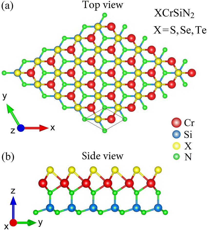 | ||
| Fig. 1 Top (a) and side (b) views of the crystal structure of XCrSiN2 (X = S, Se, Te) single-layers. | ||
| a | d Cr–X | d Cr–N | d Si–N(b) | d Si–N(m) | h | E c | C 11 | C 12 | C 66 | Y 2D | ν | |
|---|---|---|---|---|---|---|---|---|---|---|---|---|
| SCrSiN2 | 2.87 | 2.26 | 1.99 | 1.74 | 1.74 | 4.90 | −7.93 | 326.66 | 90.62 | 118.02 | 301.52 | 0.277 |
| SeCrSiN2 | 2.91 | 2.39 | 2.00 | 1.76 | 1.74 | 5.02 | −7.71 | 316.75 | 85.19 | 115.78 | 293.84 | 0.269 |
| TeCrSiN2 | 2.99 | 2.59 | 2.01 | 1.79 | 1.75 | 5.18 | −7.38 | 307.02 | 84.56 | 111.23 | 283.73 | 0.275 |
By calculating and then analyzing the cohesive energy Ecoh, the chemical bond strength is examined to confirm the structural stability of these suggested Janus structures. The cohesive energy can be calculated from the following expression
 | (1) |
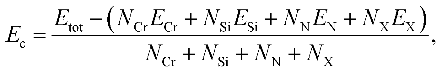
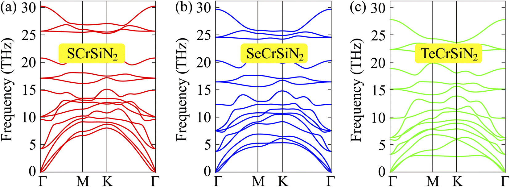
Moreover, accurate phonon calculations along the high symmetry line Γ–M–K–Γ are performed to investigate the dynamic stability of the three XCrSiN2 configurations. It is observed from Fig. 2 that there are fifteen vibrational branches (three acoustic and twelve optical modes) since there are five atoms in the primitive cell. In case the negative frequencies are available, there are no restoring forces against the atom displacement. The absence of the soft phonon modes of XCrSiN2 indicates the dynamic stability of these structures. No gap can be observed between the acoustic and optical branches demonstrating a quite high scattering process rate, i.e. the lattice thermal conductivity is relatively low. Besides, we also investigated the thermal stability of XCrSiN2 (X = S, Se, Te) structures by means of AIMD simulations at 300 K as presented in Fig. 3. It can be seen that the total potential energies in all three structures fluctuated insignificantly, about 0.3 eV, and were almost unchanged during the whole simulation. Hence, the vibration of constituent atoms is slight and only around the equilibrium positions, so that the chemical bonds remain robust.
 | ||
| Fig. 2 Phonon dispersions of (a) SCrSiN2, (b) SeCrSiN2, and (c) TeCrSiN2 single-layers. | ||
 | ||
| Fig. 3 AIMD calculations for the variations of the total energies to time of XCrSiN2 single-layers at 300 K. Insets are the crystal structures of the corresponding single layers at the end of the AIMD test. | ||
Next, the mechanical stability of Janus structures is investigated by calculating and analyzing the elastic constants in accordance with mechanical stability conditions suggested by Born and Huang.32 In general, for 2D materials, it is necessary to test four independent elastic constants, namely C11, C22, C12, and C66 (in Voigt notation). As shown in Fig. 1a, the considered material has a hexagonal structure resulting in C11 = C22. Consequently, the three following elastic constants are calculated, C11, C12 and C66, in which C66 is related to C11 and C12 by the equation C66 = (C11 − C12)/2. The obtained results Cij are tabulated in Table 1. It is found that all the elastic constants Cij decrease as the chalcogen element's atomic size increases. In more detail, C11 is ranging from 326.66 to 307.02 N m−1, C12 is ranging from 90.62 to 84.56 N m−1 and C66 is ranging from 118.02 to 111.23 N m−1 in the order of S, Se, and Te chalcogens. The elastic constants of current Janus structures XCrSiN2 meet Born–Huang's criteria for the hexagonal lattice as C11 > 0, C11 > C12, and C66 > 0,33 indicating their structures to be mechanically stable.
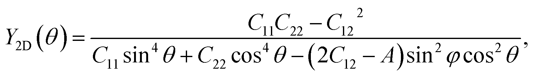
The mechanical features are also characterized by Young's modulus and Poisson's ratio, which can be calculated from Cij. The direction-dependent 2D Young's modulus (in-plane stiffness) Y2D(θ) and Poisson's ratio ν(θ) can be defined as34,35
 | (2) |
 | (3) |
 | ||
| Fig. 4 Polar diagrams for (a) Young's modulus and (b) Poisson's ratio of XCrSiN2. | ||
3.2 Electronic properties
Along with verifying the structural and dynamic stability, the electronic properties are taken into account by evaluating the band structures. In this work, both PBE and PBE + SOC functionals are utilized in order to examine precisely the energy gaps and other electronic properties of the XCrSiN2 (X = S, Se, Te) single-layers. The obtained band structures are presented in Fig. 5 and the energy bandgaps are reported in Table 2. It is calculated that the PBE bandgaps of SCrSiN2, SeCrSiN2, and TeCrSiN2 monolayers are 0.83, 0.62, and 0.16 eV, respectively. The indirect bandgap of XCrSiN2 is comparable with that of CrSi2N4 (0.49 eV). It is obvious that the band structures have the same profiles and the bandgaps calculated using PBE and PBE + SOC functionals are similar. This suggests that for these current structures, the SOC effect could be neglected to reduce computational cost without any significant difference.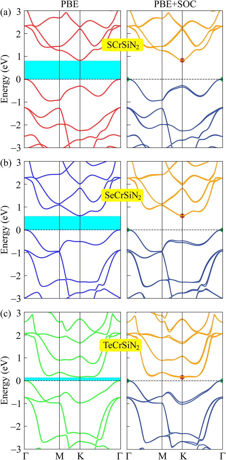 | ||
| Fig. 5 Calculated band structures of (a) SCrSiN2, (b) SeCrSiN2, and (c) TeCrSiN2 single-layers by using the PBE and PBE + SOC methods. The Fermi level is set at 0 eV. | ||
|
|
|
ΔΦ | Φ N | Φ X | |
|---|---|---|---|---|---|
| SCrSiN2 | 0.83 | 0.83 | 0.26 | 5.52 | 5.26 |
| SeCrSiN2 | 0.62 | 0.61 | 1.07 | 5.38 | 4.31 |
| TeCrSiN2 | 0.16 | 0.15 | 1.91 | 5.09 | 3.18 |
From Fig. 5, we can observe that XCrSiN2 single-layers exhibit small-bandgap semiconductor characteristics with the bandgaps decreasing as the atomic size of chalcogen X increases (S, Se, and Te). All three configurations are indirect semiconductors because the CBM and VBM are located at K and Γ points, respectively. Besides, the PBE-weighted bands of XCrSiN2 are illustrated in Fig. 6 in order to investigate the contribution of each orbital to the electronic energy bands. It can be observed that the weighted band structures of the three configurations are quite similar. The main contribution to the CBM in XCrSiN2 single-layers is the hybridization of the d-orbital of Cr with the p-orbital of S in SCrSiN2, and with the d-orbital of Se and Te in SeCrSiN2 and TeCrSiN2, respectively. However, the VBM of XCrSiN2 is contributed by the hybridization of the d-orbital of Cr with the p-orbital of N mainly, and partly with the p-orbital/d-orbital of the X atom. The Janus XCrSiN2 structures may inhibit the undesirable recombination of photoexcited electron–hole pairs due to their small energy bandgap and different atomic contributions in the CBM and VBM.
 | ||
| Fig. 6 The PBE weighted bands of (a) SCrSiN2, (b) SeCrSiN2, and (c) TeCrSiN2 single-layers. | ||
Furthermore, we calculate the work function Φ, another important feature of electrons. By calculating the electrostatic potential of the vacuum (Φvac) and of the Fermi level (ΦF), the work function Φ can be defined as Φ = Φvac − ΦF. From Table 2, the ΦN and ΦX of the three structures are not much different, implying that electrons have a comparable ability to escape from surfaces of the XCrSiN2 single-layers. Because Janus structures lack vertical mirror symmetry, inherent electric dipoles are introduced, which leads to a discrepancy in the vacuum level on the two surfaces along the z-direction, which can be characterized by ΔΦFig. 5 presents the planar electrostatic potentials of the XCrSiN2 single-layers where the dipole correction is included.37 The highest vacuum level difference between two different surfaces (ΔΦ) is found for SCrSiN2 (0.26 eV), followed by that of TeCrSiN2 (1.91 eV). The smallest work function is found for SeCrSiN2 (1.07 eV), demonstrating that the electrons can escape more easily from the surface of SeCrSiN2 than other structures. These obtained work functions are explained by the slight electronegativity difference between the N and X constituents on the two surfaces (Fig. 7).
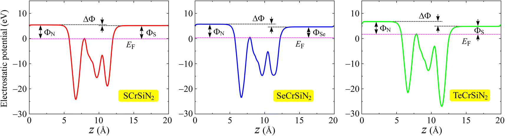 | ||
| Fig. 7 Electrostatic potentials with the dipole corrections of XCrSiN2 single-layers. The horizontal dashed line indicates the Fermi level. | ||
It is important to examine the diverse structures under various settings because, as has been reported, the physical properties, particularly the electrical characteristics, of 2D materials are easily modulated by external conditions. Among several approaches, such as doping, heterostructures, etc., strain engineering is one of the simplest but most powerful ways to modulate the electronic structures of 2D nanomaterials. The biaxial strain is defined as εb = (a − a0)/a0, where a and a0 are the length of the distorted and undistorted computed cells, respectively. In the current study, we apply a strain of from 0 to ±10%, in which compressive strain is represented by the negative sign and tensile strain by the positive sign. Previous studies38–42 indicated that the strain could result in a phase transition in 2D structures. In order to evaluate the modification of the electronic states of XCrSiN2, we applied the volumetric expansion to the unit cell of the current three structures and the tuning of electronic properties by strain εb is considered. From Fig. 8, it can be observed that the band structures of all three single-layers are altered as the biaxial strains were changed, where the notable change is found to be near the Fermi levels. Fig. 9a depicts the dependence of energy bandgap on the biaxial strain. When the compressive strain increases, the energy bandgaps of both SCrSiN2 and SeCrSiN2 increase, up to about 1.7 and 1.0 eV, respectively. However, for TeCrSiN2, the energy bandgap is almost unchanged when the compressive strain is lower than 10%; and as εb = −10%, the energy bandgap is nearly zero, i.e., there is a transition from a small-bandgap to zero-bandgap semiconductor in TeCrSiN2. When there is tensile strain, the energy bandgap of SCrSiN2 is rapidly decreased (about 0.2 eV as εb = 10%); that of SeCrSiN2 is reduced as well (about 0.5 eV as εb = 10%), and that of TeCrSiN2 is insignificantly changed.
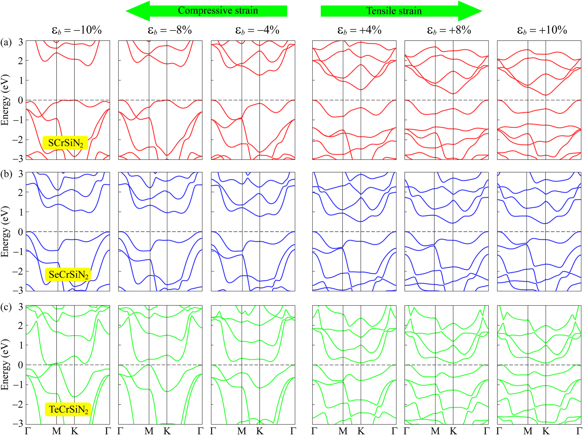 | ||
| Fig. 8 Band structures of (a) SCrSiN2, (b) SeCrSiN2, and (c) TeCrSiN2 under the biaxial strains εb. | ||
 | ||
| Fig. 9 Bandgaps of XCrSiN2 as functions of the biaxial strain (a) and external electric field (b). | ||
For further investigating the alternative electronic structures under different conditions, besides volumetric strain, an external electric field is next employed to control the electronic structure of examined single-layers. In our modeling, an external electric field is set perpendicular to the 2D plane of materials. The electric field intensity is from −5 V nm−1 to +5 V nm−1. The positive (negative) electric fields indicate that the direction is along (opposite to) the positive z-axis. The obtained calculations for energy bandgaps are plotted in Fig. 9b. It can be seen that bandgaps of all three single layers are hardly changed when the electric field is introduced. These results are derived from the band structure calculations (not shown here) in which there is a weak dependence of the band structure on the electric field.
3.3 Carrier mobility
The carrier mobilities and transport characteristics of XCrSiN2 are explored in the final section to examine the migration and separation mechanisms. The suitability of a material for use in electrical devices is mostly determined by the mobility of carriers, especially electrons. It is well-known that there are many efficient ways to calculate carrier mobility, such as deformation potential approximation30 and Boltzmann transport theory.43 It should be emphasized that electron-phonon coupling (EPC) is significant in influencing the physical characteristics of materials, particularly thermoelectric properties and thermal conductivity.44,45 In the present work, we only use the deformation potential (DP) approximation to evaluate the mobility of carriers. In the DP theory, the carrier mobility for 2D materials μ2D is given by:46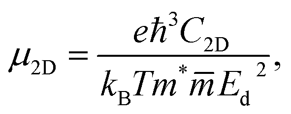 | (4) |
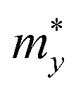
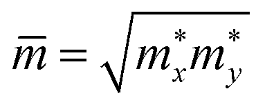 refers to the average effective mass. The DP constant Ed and elastic modulus C2D are obtained by calculating the band edges and total energy, respectively, with respect to the uniaxial strain. The m* of the carriers is calculated based on the dispersion of the CBM and VBM. The more dispersive area, the smaller the effective mass. In this study, the temperature T is set to be 300 K. All of the calculated values of effective mass, elastic modulus, DP constant, and mobility of carriers along the x and y directions are tabulated in Table 3.
|
|
|
|
|
|
|
μ x (cm2 V−1 s−1) | μ y (cm2 V−1 s−1) | ||
|---|---|---|---|---|---|---|---|---|---|
| Electron | SCrSiN2 | 1.08 | 1.16 | 420.84 | 420.99 | −10.49 | −10.49 | 67.01 | 62.80 |
| SeCrSiN2 | 1.53 | 1.59 | 403.19 | 403.54 | −10.04 | −10.04 | 35.62 | 34.44 | |
| TeCrSiN2 | 5.36 | 4.78 | 385.82 | 386.14 | −9.79 | −9.79 | 3.15 | 3.53 | |
| Hole | SCrSiN2 | 2.98 | 2.86 | 420.84 | 420.99 | −5.94 | −5.96 | 29.16 | 30.36 |
| SeCrSiN2 | 3.21 | 3.03 | 403.19 | 403.54 | −6.77 | −6.77 | 18.74 | 19.83 | |
| TeCrSiN2 | 3.14 | 2.92 | 385.82 | 386.14 | −8.66 | −8.66 | 11.49 | 12.41 |


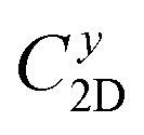
The small uniaxial strain εuni (from −0.4 to +0.4%) is used to estimate the changing of total energy and the band edge positions. Fig. 10 illustrates the dependence of the total energies and the energies at the band edges on uniaxial strain εuni. From Fig. 10a, the total energies are found to alter insignificantly when the small uniaxial strain εuni is applied in the x− or y− direction and has similar values in both directions. As for the elastic modulus, the highest value C2D is found for SMoSiN2, followed by that of SeMoSiN2, then of TeMoSiN2. It can be seen that for each structure, the elastic modulus  and
and  are nearly equal; in other words, the elastic modulus is essentially independent of the directions of uniaxial strains. However, it can be observed from Fig. 10b that the band edge positions of XMoSiN2 are almost the same along the directions of uniaxial strains. The deformation potential constants Ed listed in Table 3 indicate that for both electron and hole carriers, Ed is quite isotropic with the two in-plane transport directions. Consequently, the carrier mobilities are expected to be directional isotropy with the x and y transport directions.
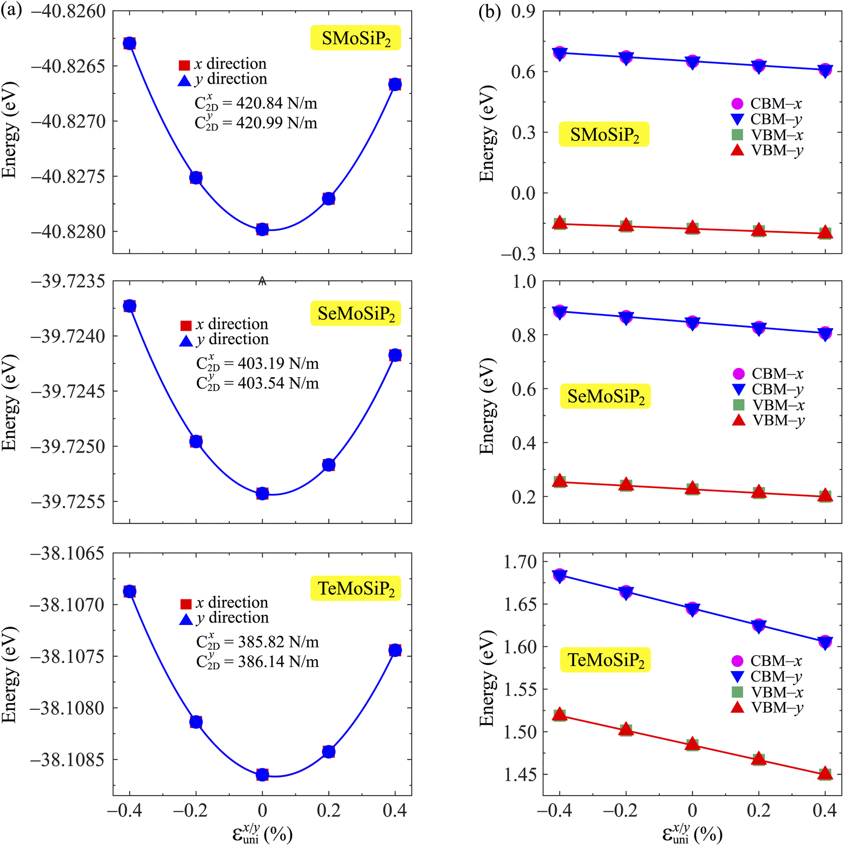 | ||
Fig. 10 The uniaxial strain-dependence 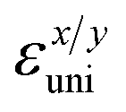 of the total energies (a) and energies at the band edges (b) of XCrSiN2 single-layers. Fitted data are shown by the solid line. of the total energies (a) and energies at the band edges (b) of XCrSiN2 single-layers. Fitted data are shown by the solid line. | ||
Concerning directional isotropy, electron and hole mobilities for the x direction and y direction are similar. The electron mobilities in SCrSiN2 and SeCrSiN2 are much higher [67.01 (62.08) and 35.62 (34.44) cm2 V−1 s−1 along the x− (y−) direction] than that in TeCrSiN2 [3.15 (3.53) cm2 V−1 s−1 along the x− (y−) direction]. As for hole mobilities, in both directions, higher values are found for the holes in the VBM of SCrSiN2 and SeCrSiN2, followed by that of TeCrSiN2. These obtained mobilities demonstrate that the electrons and holes in SCrSiN2 are all fast carriers with the highest migration abilities among the carriers in the three materials. Moreover, it is worth noting that in SCrSiN2 and SeCrSiN2 structures, the mobilities of electrons are greater than those of holes. However, in SeCrSiN2 structures, it can be seen that the hole mobilities are higher compared to electron mobilities. This is mainly due to the differences of structural and chemical structures, specifically, the differences of dispersion profiles in the CBM and VBM in XCrSiN2 single-layers as shown in Fig. 5 and 6; hence, the effective mass of electrons and holes is affected.
4 Conclusive remarks
In the current work, we explored the stabilities of the crystal structure, electronic properties, and transport features of the new quintuple XCrSiN2 single-layers. The results show that the proposed Janus single-layers are energetically and thermally stable that reveal the potential to fabricate experimentally. All three structures exhibit semiconducting behavior with small indirect bandgaps. When biaxial strain is applied, the electronic structures of the Janus XCrSiN2 single-layers are modulated significantly, especially, at εb = −10%, and those of SCrSiN2 single-layers are transmitted from the semiconductor to metal. Meanwhile, it is found that these proposed structures show weak dependence of their electronic bands on the electric field. The mobilities of electrons and holes are calculated indicating the highly directional isotropy due to the similarity in the effective masses. The mobility of electrons is higher than that of holes in SCrSiN2 and SeCrSiN2. The calculated results for mobility are found to be opposite for the TeCrSiN2 case. Our proposed Janus quintuple XCrSiN2 single-layers are promising 2D materials in the future with various applications.Conflicts of interest
There are no conflicts of interest to declare.Acknowledgements
This research was funded by the Vietnam Ministry of Education and Training under grant no. B2022-DNA-14.References
- Y. Guo, S. Zhou, Y. Bai and J. Zhao, Appl. Phys. Lett., 2017, 110, 163102 CrossRef.
- A. Kandemir and H. Sahin, Phys. Rev. B, 2018, 97, 155410 CrossRef CAS.
- Y. Bai, Q. Zhang, N. Xu, K. Deng and E. Kan, Appl. Surf. Sci., 2019, 478, 522–531 CrossRef CAS.
- W. Zhou, J. Chen, Z. Yang, J. Liu and F. Ouyang, Phys. Rev. B, 2019, 99, 075160 CrossRef.
- T. V. Vu, H. V. Phuc, A. I. Kartamyshev and N. N. Hieu, Appl. Phys. Lett., 2023, 122, 061601 CrossRef CAS.
- M.-Y. Liu, Y. He, X. Li and K. Xiong, Phys. Chem. Chem. Phys., 2023, 25, 7278–7288 RSC.
- Y. Dahiya, M. Hariram, M. Kumar, A. Jain and D. Sarkar, Coord. Chem. Rev., 2022, 451, 214265 CrossRef CAS.
- L. Banszerus, M. Schmitz, S. Engels, J. Dauber, M. Oellers, F. Haupt, K. Watanabe, T. Taniguchi, B. Beschoten and C. Stampfer, Sci. Adv., 2015, 1, e1500222 CrossRef PubMed.
- N. A. Poklonski, S. A. Vyrko, A. I. Siahlo, O. N. Poklonskaya, S. V. Ratkevich, N. N. Hieu and A. A. Kocherzhenko, Mater. Res. Express, 2019, 6, 042002 CrossRef.
- Q. H. Wang, K. Kalantar-Zadeh, A. Kis, J. N. Coleman and M. S. Strano, Nat. Nanotechnol., 2012, 7, 699 CrossRef CAS PubMed.
- C. V. Nguyen, N. N. Hieu, N. A. Poklonski, V. V. Ilyasov, L. Dinh, T. C. Phong, L. V. Tung and H. V. Phuc, Phys. Rev. B, 2017, 96, 125411 CrossRef.
- N. N. Hieu, H. V. Phuc, V. V. Ilyasov, N. D. Chien, N. A. Poklonski, N. V. Hieu and C. V. Nguyen, J. Appl. Phys., 2017, 122, 104301 CrossRef.
- A. V. Lugovskoi, M. I. Katsnelson and A. N. Rudenko, Phys. Rev. Lett., 2019, 123, 176401 CrossRef CAS PubMed.
- V. T. Vi, N. N. Hieu, B. D. Hoi, N. T. Binh and T. V. Vu, Superlattices Microstruct., 2020, 140, 106435 CrossRef CAS.
- K. D. Pham, V. T. Vi, D. V. Thuan, N. V. Hieu, C. V. Nguyen, H. V. Phuc, B. D. Hoi, L. T. Phuong, N. Q. Cuong, D. V. Lu and N. N. Hieu, Chem. Phys., 2019, 524, 101–105 CrossRef CAS.
- F.-f. Zhu, W.-j. Chen, Y. Xu, C.-l. Gao, D.-d. Guan, C.-h. Liu, D. Qian, S.-C. Zhang and J.-f. Jia, Nat. Mater., 2015, 14, 1020–1025 CrossRef CAS PubMed.
- A. Acun, L. Zhang, P. Bampoulis, M. Farmanbar, A. van Houselt, A. N. Rudenko, M. Lingenfelder, G. Brocks, B. Poelsema, M. I. Katsnelson and H. J. W. Zandvliet, J. Phys.: Condens. Matter, 2015, 27, 443002 CrossRef CAS PubMed.
- N. N. Hieu, H. V. Phuc, A. I. Kartamyshev and T. V. Vu, Phys. Rev. B, 2022, 105, 075402 CrossRef CAS.
- T. V. Vu, V. T. T. Vi, H. V. Phuc, A. I. Kartamyshev and N. N. Hieu, Phys. Rev. B, 2021, 104, 115410 CrossRef CAS.
- S.-D. Guo, W.-Q. Mu, Y.-T. Zhu, R.-Y. Han and W.-C. Ren, J. Mater. Chem. C, 2021, 9, 2464–2473 RSC.
- T. V. Vu and N. N. Hieu, J. Condens.: Matter Phys., 2021, 34, 115601 CrossRef PubMed.
- H. Zhou, H. Tang, H. Yuan and H. Chen, J. Magn. Magn. Mater., 2022, 562, 169742 CrossRef CAS.
- Y. Gao, J. Liao, H. Wang, Y. Wu, Y. Li, K. Wang, C. Ma, S. Gong, T. Wang, X. Dong, Z. Jiao and Y. An, Phys. Rev. Appl., 2022, 18, 034033 CrossRef CAS.
- S.-T. Nguyen, C. Q. Nguyen, Y. S. Ang, H. V. Phuc, N. N. Hieu, N. T. Hiep, N. M. Hung, L. T. T. Phuong, N. V. Hieu and C. V. Nguyen, J. Phys. D: Appl. Phys., 2022, 56, 045306 CrossRef.
- P. Giannozzi, S. Baroni, N. Bonini, M. Calandra, R. Car, C. Cavazzoni, D. Ceresoli, G. L. Chiarotti, M. Cococcioni, I. Dabo, A. D. Corso, S. de Gironcoli, S. Fabris, G. Fratesi, R. Gebauer, U. Gerstmann, C. Gougoussis, A. Kokalj, M. Lazzeri, L. Martin-Samos, N. Marzari, F. Mauri, R. Mazzarello, S. Paolini, A. Pasquarello, L. Paulatto, C. Sbraccia, S. Scandolo, G. Sclauzero, A. P. Seitsonen, A. Smogunov, P. Umari and R. M. Wentzcovitch, J. Phys.: Condens. Matter, 2009, 21, 395502 CrossRef PubMed.
- J. P. Perdew, K. Burke and M. Ernzerhof, Phys. Rev. Lett., 1996, 77, 3865 CrossRef CAS PubMed.
- H. J. Monkhorst and J. D. Pack, Phys. Rev. B, 1976, 13, 5188–5192 CrossRef.
- S. Grimme, J. Antony, S. Ehrlich and H. Krieg, J. Chem. Phys., 2010, 132, 154104 CrossRef PubMed.
- S. Nosé, J. Chem. Phys., 1984, 81, 511 CrossRef.
- J. Bardeen and W. Shockley, Phys. Rev., 1950, 80, 72 CrossRef CAS.
- L. Wang, Y. Shi, M. Liu, A. Zhang, Y.-L. Hong, R. Li, Q. Gao, M. Chen, W. Ren, H.-M. Cheng, Y. Li and X.-Q. Chen, Nat. Commun., 2021, 12, 2361 CrossRef CAS PubMed.
- M. Born and K. Huang, Am. J. Phys., 1955, 23, 474 CrossRef.
- R. C. Andrew, R. E. Mapasha, A. M. Ukpong and N. Chetty, Phys. Rev. B, 2012, 85, 125428 CrossRef.
- N. T. Hung, A. R. T. Nugraha and R. Saito, J. Phys. D: Appl. Phys., 2018, 51, 075306 CrossRef.
- P. Xiang, S. Sharma, Z. M. Wang, J. Wu and U. Schwingenschlögl, ACS Appl. Mater. Interfaces, 2020, 12, 30731 CrossRef CAS PubMed.
- D. G. Pettifor, Mater. Sci. Technol., 1992, 8, 345–349 CrossRef CAS.
- L. Bengtsson, Phys. Rev. B, 1999, 59, 12301 CrossRef CAS.
- H. Liu, Z. Huang, C. He, Y. Wu, L. Xue, C. Tang, X. Qi and J. Zhong, J. Appl. Phys., 2018, 125, 082516 CrossRef.
- D. Q. Khoa, D. T. Nguyen, C. V. Nguyen, V. T. Vi, H. V. Phuc, L. T. Phuong, B. D. Hoi and N. N. Hieu, Chem. Phys., 2019, 516, 213–217 CrossRef CAS.
- T. V. Vu, V. T. T. Vi, C. V. Nguyen, H. V. Phuc and N. N. Hieu, J. Phys. D: Appl. Phys., 2020, 53, 455302 CrossRef CAS.
- T. V. Vu, V. T. T. Vi, H. V. Phuc, C. V. Nguyen, N. A. Poklonski, C. A. Duque, D. P. Rai, B. D. Hoi and N. N. Hieu, J. Phys.: Condens. Matter, 2021, 33, 225503 CrossRef CAS PubMed.
- T. V. Vu, C. V. Nguyen, H. V. Phuc, A. A. Lavrentyev, O. Y. Khyzhun, N. V. Hieu, M. M. Obeid, D. P. Rai, H. D. Tong and N. N. Hieu, Phys. Rev. B, 2021, 103, 085422 CrossRef CAS.
- B. Zeng, M. Li, X. Zhang, Y. Yi, L. Fu and M. Long, J. Phys. Chem. C, 2016, 120, 25037–25042 CrossRef CAS.
- S. Qi, J. Liu, Y. Li and M. Zhao, Phys. Rev. B, 2022, 106, 165204 CrossRef CAS.
- A. Giri, P. Karna and P. E. Hopkins, J. Phys. Chem. Lett., 2022, 13, 10918–10923 CrossRef CAS PubMed.
- W. Wan, S. Zhao, Y. Ge and Y. Liu, J. Phys.: Condens. Matter, 2019, 31, 435501 CrossRef CAS PubMed.
| This journal is © The Royal Society of Chemistry 2023 |