
 Open Access Article
 This Open Access Article is licensed under a
 Creative Commons Attribution 3.0 Unported Licence
Edge contacts accelerate the response of MoS2 photodetectors†
Fabian
Strauß
ab,
Christine
Schedel
a and
Marcus
Scheele
 *ab
*ab
aInstitute of Physical and Theoretical Chemistry, University of Tübingen, Auf der Morgenstelle 18, 72076 Tübingen, Germany. E-mail: marcus.scheele@uni-tuebingen.de
bLISA+, University of Tübingen, Auf der Morgenstelle 15, 72076 Tübingen, Germany
First published on 5th June 2023
Abstract
We use a facile plasma etching process to define contacts with an embedded edge geometry for multilayer MoS2 photodetectors. Compared to the conventional top contact geometry, the detector response time is accelerated by more than an order of magnitude by this action. We attribute this improvement to the higher in-plane mobility and direct contacting of the individual MoS2 layers in the edge geometry. With this method, we demonstrate electrical 3 dB bandwidths of up to 18 MHz which is one of the highest values reported for pure MoS2 photodetectors. We anticipate that this approach should also be applicable to other layered materials, guiding a way to faster next-generation photodetectors.
Introduction
The rise of 2D materials in optoelectronics has led to remarkable research results in recent years, from ultra-thin transistors1,2 to single-layer light-emitting diodes3 and novel photodetectors.4,5 For the latter, two properties are of particular interest: device responsivity and device speed. For high frequency applications, silicon and InGaAs are the most advanced materials today,6 but they are starting to reach physical limits. A possible alternative is found in layered materials. The intrinsic photoresponse of these layered materials such as graphene or transition metal dichalcogenides (TMDCs) has revealed response times in the picosecond regime.7 This intrinsic response is a measure for the pure, material-specific photoresponse and defines an upper limit for an ideal photodetector, in which the speed is solely limited by the active material. However, in most devices the actual speed is furthermore affected by extrinsic properties related to the device geometry, such as the RC- or transit time. Pure TMDC devices exhibit typical response times ranging from milliseconds8,9 to seconds,8–10 with a few fast devices in the microsecond range7–9,11,12 and even less in the sub-microsecond regime.13 Many methods have been used in the search for ultrafast photodetectors based on nanomaterials: chemical doping,14 heterojunction implementation,15,16 photonic waveguide integration,17 and small channel lengths,18,19 to name a few. In addition, parameters such as the choice of substrate,18,20 interface roughness,21 electrode material,10,22,23 and geometry13,24,25 or environment26,27 must be considered each time.Traditionally, top contacts above, or bottom contacts below the active material are used for nanomaterial photodetectors. More advanced structures can also be built by a vertical arrangement of electrodes and desired material.13,19 In addition, layered materials can be contacted at the edge of the flake.28,29 Thereby, instead of touching the surface of the layered material, cf.Fig. 1a, the edge of a flake is uncovered, for example with etching,29,30 and the electrodes are evaporated on the edge of the material, cf.Fig. 1b.
 | ||
| Fig. 1 Schematic of an (a) top contacted and (b) edge contacted MoS2 crystal. (c) SEM image of an etched MoS2 flake. | ||
An SEM-image of an etched flake showing the exposed edge of a MoS2 flake can be seen in Fig. 1c and SI2.† These one-dimensional edge contacts have attracted much attention in recent years. They are being investigated for their reduced transfer length,31,32 lower contact resistance,28,33–35 better control of the Schottky barrier36,37 higher capability of charge injection37,38 or Fermi level depinning,28,30,36 to name a few examples. However, to our knowledge, the effect of edge contacts on the response time properties of TMDC photodetectors is still unknown.
In this work, we investigate the difference between edge electrodes and conventional top electrodes and their influence on the response speed of pure MoS2 photodetectors. The MoS2 flakes studied here were exfoliated using a standard scotch tape/PDMS exfoliation method.29 They are between 50 and 200 nm thick, see Fig. SI1e,† and can thus be considered bulk crystals where the height no longer affects the properties.12
We show that the electrode geometry of the device – edge electrodes instead of top contacts – accelerate the decay time by at least an order of magnitude. Primarily, we have studied the steady state photoresponse towards a 635 nm square pulse with some additional non-steady state measurements towards a 636 nm impulse laser. By using these techniques, pure MoS2 devices can be realized with one of the highest recorded bandwidths of more than 18 MHz. We hypothesize that this geometry should be particularly advantageous for TMDCs in view of the much more efficient in-plane transport compared to transport across several van-der-Waals layers.
Experimental section
Fabrication
MoS2 detectors were fabricated by exfoliating TMDC flakes with scotch tape onto cleaned glass substrates functionalized with HMDS. For the bottom contacts, the flakes were stamped directly onto lithographically fabricated electrodes (2.5–20 × 80 μm). For all other electrode geometries, optical lithography was performed directly on the flakes using a maskless aligner (μMLA Heidelberg Instruments). For the edge contacts, an additional plasma etching step is performed before vapor deposition of the electrode material. The platelets were etched with a mixture of O2/SF6 plasma (100 W, 25% O2/75% SF6, 50 mTorr, 20 s). The electrode material, e.g., 4 nm Ti and 20 nm Au, was evaporated at a pressure of <2 × 10⁻⁶ mbar. The detectors were examined under atmospheric conditions.For the Ti![[thin space (1/6-em)]](https://www.rsc.org/images/entities/char_2009.gif) :Au top contacts as well as the Au edge electrodes, 4 nm Ti and 20 nm Au were evaporated. For the Ti edge contacts, 20 nm Ti and 4 nm Au or only 25 nm Ti were evaporated. Since they have shown similar behavior, their data is shown jointly. The Au bottom contacts are made of 4 nm Ti and 20 nm Au and the Ti bottom contacts of 25 nm Ti.
:Au top contacts as well as the Au edge electrodes, 4 nm Ti and 20 nm Au were evaporated. For the Ti edge contacts, 20 nm Ti and 4 nm Au or only 25 nm Ti were evaporated. Since they have shown similar behavior, their data is shown jointly. The Au bottom contacts are made of 4 nm Ti and 20 nm Au and the Ti bottom contacts of 25 nm Ti.
Transient photoresponse
Time-resolved photocurrent measurements were performed at room temperature in a Lake Shore Cryotronics CRX-6.5K probe station. Square pulse illumination of the photodetectors was used to measure the steady state photoelectric response. For this, a fast-switching laser driver (FSL500, PicoQuant), driven by a Hewlett Packard 33120A arbitrary waveform generator was used. The 635 nm laser diode has an optical output power of ≤12 mW and a laser rise time of <0.5 ns. The non-steady state photoresponse of the detectors was investigated with a picosecond pulsed laser driver (Taiko PDL M1, PicoQuant) utilizing a 636 nm laser head with a pulse width <500 ps. For a repetition rate of 100 kHz, an average optical power of 22 μW was chosen. The laser powers were further reduced due to decollimation of the beam, inefficient coupling into the optical fiber and scattering. An unfocused beam was used with a laser spot larger than the detector area.50 Ω matched tungsten probes and 40 GHz coaxial cables as short as possible were used to contact the detector with the external circuit. A transimpedance amplifier (FEMTO DHPCA-100) was used to preamplify the current before measuring with a Zurich Instruments UHFLI lock-in amplifier with a Periodic Waveform Analyzer function averaging the signal from 2 G samples. Before further analysis, the signals were background corrected. The bandwidth of the lock-in amplifier is 600 MHz which is further reduced to 14–200 MHz by the variable gain transimpedance amplifier.
For some contacts, the Fourier transform of 100 kHz measurements was performed after applying zero padding to mimic a 25 kHz measurement and determine the 3 dB bandwidth.
Results and discussion
Steady state photoresponse of edge and top contacted MoS2
Square pulse laser measurements determine the rise time to reach steady state as well as the corresponding fall time. This allows investigating the influence of changing the electrode geometry and/or the contacting metal for both parameters, which we used to study the effect of an edge contact compared to titanium:gold top electrodes (Ti:Au top). For further information and a scheme of the measurement setup used, the interested reader is referred to our previous work.18
The edge geometry is either fabricated with the same ratio of Ti:Au (Au edge) or with the inverted ratio of titanium and gold (Ti edge), referring to the predominant contacting metal. See Fig. SI3† for the fabrication process. Typical square pulse responses of these three geometries are shown in Fig. 2a.
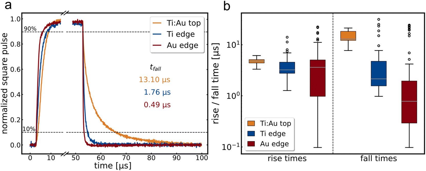 | ||
| Fig. 2 (a) Normalized square pulse response of a top contact (ochre), a titanium edge contact (blue) and a gold edge contact (red). All measurements performed with a 635 nm square pulse laser with 10 kHz repetition rate, 15 μm channel length, 0.1 V bias applied. (b) Box-and-whisker-plots of all 10 kHz, 635 nm square pulse measurements for each electrode configuration. The left half displays the rise times, and the right half the fall times. Measurements of 18 Ti:Au top, 74 Au edge, 46 Ti edge measurements contacts are included at various bias voltages between −1 and 1 V. | ||
The fall time accelerates tremendously for the edge geometry, while the rise time accelerates only slightly. We attribute this result predominantly to the geometry but note that the metal also plays an important role. The significance of each effect can be seen in Fig. 2b, which shows the box-and-whisker plots across all 10 kHz square pulse measurements for all investigated Ti:Au top and Ti and Au edge contact flakes (4 Ti:Au top, 8 Au edge, 5 Ti edge contacts; 18 Ti:Au top, 74 Au edge, 46 Ti edge measurements). Thereby, the box includes all values from the first to the third quartile, while the whiskers span to the value maximal 1.5 times the box size away. Every value exceeding this range is displayed as an outlier. Again, the rise time does not show much improvement in the median values, although some contacts display much faster rise times for the edge contact compared to the top contacts. In contrast, the fall time shows a massive acceleration for the edge contacts, an improvement of at least a factor of eleven for the mean value compared to the top contacts. This uneven acceleration can be attributed to the multiple mechanisms that play a role in the rise time compared to the fall time, like generation of electron–hole pairs. The large spread in the Au edge data is caused by the slightly bigger sample size, a pronounced persistent photocurrent effect for especially higher bias voltages,39cf. Fig. SI4,† and the specific challenges of the fabrication of edge contacts: as can be seen in Fig. 1c, the etched flank is bolt upright, but it has a slight tendency to be tilted either inwards or outwards, thereby changing the contact angle for the edge electrodes and thus the quality of the contact. To further improve the edge contact in the future, more dedicated procedures like the etching process by Cheng et al.31 may be beneficial, which has the benefit to produce edge contacts with greater reliability and control over the environment.
We attribute the accelerated response times to the improved contacting method. Conventional top contacts with vapor deposited electrodes have many defects and hybridization in the first layers,40 eliminating the van der Waals gap between the electrode and TMDC. Underneath, however, are many more layers with vdW gaps and thus tunnelling barriers that must be overcome to inject a charge carrier into the electrode. In the geometry of the edge electrodes, (nearly) all layers are contacted and charge transport to the contact occurs in the plane of the MoS2 crystal, which has much higher mobilities.41 This greatly enhances the carrier injection.28 Moreover, the edge contacts may form covalent bonds with the dangling bonds of the TMDCs,28 which further improve charge transport.
In addition to the different electrode geometry, the contacting metal has also been shown to have an impact on device speed. To quantify this influence, MoS2 flakes were investigated in a bottom electrode geometry with either titanium or gold as contact material (see Fig. 3a).
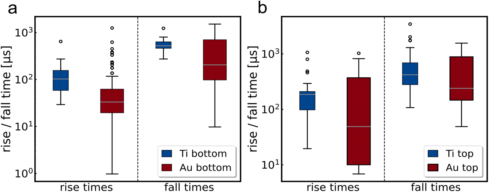 | ||
| Fig. 3 Box-and-whisker plots of rise and fall times of MoS2 flakes contacted with either titanium (blue) or gold (red). (a) Bottom electrode geometry, (b) top electrodes where the different channels on the same flake are contacted with titanium or gold. All measurements are carried-out with a 635 nm laser and a repetition rate of 100 Hz. | ||
In addition, an analysis was performed by patterning the same flake twice so that some channels were contacted with the Ti:Au top electrodes and others with Au top electrodes only (see Fig. 3b). Both sets of experiments show the same trend already observed in the edge contact experiments, namely an acceleration of the rise and fall times with gold as the contact metal. However, the mean value of all Ti edge contacts is still faster than the best top contacts, demonstrating that the contact geometry remains an important factor for the overall response speed of the MoS2 photodetectors.
The influence of the contacting metal on the electrical or optoelectrical behaviour of materials is not new and has been detailed for instance in the work of Jain et al.42 Nevertheless, it is often discussed only in terms of contact resistance or dark currents, cf. Fig. SI5,† but rarely in terms of response times. For TMDCs, a study by Zhang et al.22 already investigated the rise time effects of palladium and titanium contacts on WSe2. The authors explained the faster response for titanium with a higher Schottky barrier. In the case of Au, Ti, and MoS2, the respective work functions are about 5.4 eV,43 4.3 eV,44 and44 3.9 eV (ref. 45) for the edge facet of MoS2 or 5.4 eV (ref. 46) for the top facet. Thus, regarding the titanium gold comparison, the higher Schottky barrier is expected for Au contacts, which are shown to be faster in the experiments.38 Furthermore, in a comparison of Au with the corresponding work functions of MoS2, again, the higher Schottky barrier is found for the faster contact geometry – edge contacts, cf. Fig. SI6.† A detailed analysis of the work functions in the different contact geometries shown here is beyond the scope of this work and would require surface tunnelling spectroscopy or similar methods.
With respect to the limiting mechanism of edge and top contact we performed measurements at different voltages which could provide hints towards a transit time limitation. Additional measurements with different channel lengths in the range from 2.5 μm to 20 μm could give further information on either a transit time limited mechanism or an RC-time limit in case of no voltage dependency. Both, voltage, and channel length variation do not show any trend, cf. Fig. SI7 and SI8,† thereby a limiting mechanism cannot be determined. Further distinctions towards an RC limitation would require impedance measurements.
In summary, MoS2 detectors can be accelerated enormously by using edge contacts in comparison to top contacts, cf. Ti:Au top and Ti edge in Fig. 2a. An additional tuning by using an appropriate electrode metal as already announced in literature can further help to accelerate the detector especially in the fall times, as shown by using Au edge electrodes.
Non-steady state photoresponse of edge and top contacted MoS2
The investigation with a delta-shaped laser pulse mimics the data transmission in optical fibres and is therefore of relevance to determine the bandwidth of the device. For this purpose, the impulse response (f(t)) must be Fourier transformed (FFT) to obtain the power spectrum (P(ω)): P(ω) = |FFT(f(t))|2 After normalization with the steady-state power (P1), the bandwidth spectrum can be converted to dB = 10log10(P(ω)/P1). The 3 dB bandwidth is then a measure of the frequency at which the power of the signal drops to half its value.
Most flakes have relatively little signal, so it is not possible to determine the impulse photoresponse for each bias voltage and channel. Thus, no further information about the limiting mechanism can be obtained, only a representative trend, which can be seen in Fig. 4.
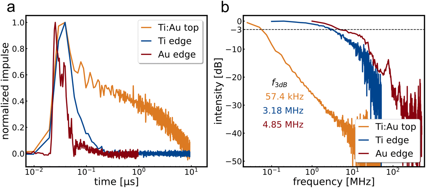 | ||
| Fig. 4 (a) Normalized impulse photoresponse of a Ti:Au top (ochre), a titanium edge (blue) and a gold edge (red) contacted MoS2 device towards a 636 nm pulsed laser. Measured are 10 μm contacts under a 1 V bias with either 100 kHz for the Ti edge and Ti:Au top device or 1 MHz for the Au edge device. (b) Fourier transformed impulse response to determine the 3 dB bandwidth of the device. For the top contact zero-padding is performed to mimic a quasi 25 kHz measurement. | ||
Fig. 4a shows exemplary impulse responses of the three types of detectors investigated and Fig. 4b the corresponding bandwidth spectra obtained by fast Fourier transform. As with the steady-state measurements, the trend shows the acceleration of the bandwidth when using edge contacts by a factor of more than 80 times for the example shown. The fastest device response exceeding a bandwidth of 18 MHz can be seen in Fig. SI9.†
Conclusions
In summary, we have demonstrated the accelerating effect of edge contacts for the response of MoS2 photodetectors compared to the conventionally used top contacts. This improvement is caused by the better charge carrier injection into the electrodes due to the higher in-plane mobility compared to the out-of-plane mobility of TMDCs. In addition, the contacting metal and the associated Schottky barrier play an important role: for MoS2, gold leads to faster rise and fall times than titanium. By combining these two effects, we have built photodetectors with a bandwidth as high as 18 MHz, which, to the best of our knowledge, surpasses all neat MoS2 photodetectors developed so far. We believe that the implementation of edge contacts in photodetectors made of 2D materials has great potential due to their scalability and simplicity.Conflicts of interest
There are no conflicts to declare.Acknowledgements
We thank Elke Nadler for the SEM images. Furthermore, we acknowledge Prof. Alfred J. Meixner and Prof. Monika Fleischer for the provision of their laboratory space and Olympia Geladari for the support with the exfoliation process. Financial support of this work has been provided by the European Research Council (ERC) under the European Union's Horizon 2020 research and innovation program (Grant Agreement 802822) as well as the DFG under grant SCHE1905/9-1.References
- B. Radisavljevic, A. Radenovic, J. Brivio, V. Giacometti and A. Kis, Nat. Nanotechnol., 2011, 6, 147–150 CrossRef CAS PubMed.
- H. Yang, S. Cai, Y. Zhang, D. Wu and X. Fang, J. Phys. Chem. Lett., 2021, 12, 2705–2711 CrossRef CAS PubMed.
- R. S. Sundaram, M. Engel, A. Lombardo, R. Krupke, A. C. Ferrari, P. Avouris and M. Steiner, Nano Lett., 2013, 13, 1416–1421 CrossRef CAS PubMed.
- Z. Yin, H. Li, H. Li, L. Jiang, Y. Shi, Y. Sun, G. Lu, Q. Zhang, X. Chen and H. Zhang, ACS Nano, 2012, 6, 74–80 CrossRef CAS PubMed.
- V. W. Brar, M. C. Sherrott and D. Jariwala, Chem. Soc. Rev., 2018, 47, 6824–6844 RSC.
- N. Huo and G. Konstantatos, Adv. Mater., 2018, 30, 1801164 CrossRef PubMed.
- H. Wang, C. Zhang, W. Chan, S. Tiwari and F. Rana, Nat. Commun., 2015, 6, 8831 CrossRef CAS PubMed.
- R. Wadhwa, A. v. Agrawal and M. Kumar, J. Phys. D: Appl. Phys., 2021, 55, 063002 CrossRef.
- A. Taffelli, S. Dirè, A. Quaranta and L. Pancheri, Sensors, 2021, 21, 2758 CrossRef CAS PubMed.
- O. Lopez-Sanchez, D. Lembke, M. Kayci, A. Radenovic and A. Kis, Nat. Nanotechnol., 2013, 8, 497–501 CrossRef CAS PubMed.
- D. S. Tsai, K. K. Liu, D. H. Lien, M. L. Tsai, C. F. Kang, C. A. Lin, L. J. Li and J. H. He, ACS Nano, 2013, 7, 3905–3911 CrossRef CAS PubMed.
- W. Tang, C. Liu, L. Wang, X. Chen, M. Luo, W. Guo, S. W. Wang and W. Lu, Appl. Phys. Lett., 2017, 111, 153502 CrossRef.
- D. Maeso, A. Castellanos-Gomez, N. Agraït and G. Rubio-Bollinger, Adv. Electrode Mater., 2019, 5, 1900141 CrossRef.
- Z. Hu, Z. Wu, C. Han, J. He, Z. Ni and W. Chen, Chem. Soc. Rev., 2018, 47, 3100–3128 CAS.
- P. v. Pham, S. C. Bodepudi, K. Shehzad, Y. Liu, Y. Xu, B. Yu and X. Duan, Chem. Rev., 2022, 122, 6514–6613 CrossRef CAS PubMed.
- S. Saggar, S. Sanderson, D. Gedefaw, X. Pan, B. Philippa, M. R. Andersson, S. C. Lo and E. B. Namdas, Adv. Funct. Mater., 2021, 31, 2010661 CrossRef CAS.
- J. F. Gonzalez Marin, D. Unuchek, K. Watanabe, T. Taniguchi and A. Kis, npj 2D Mater. Appl., 2019, 3, 14 CrossRef.
- C. Schedel, F. Strauß, K. Kumar, A. Maier, K. M. Wurst, P. Michel and M. Scheele, ACS Appl. Mater. Interfaces, 2021, 13, 47954–47961 CrossRef CAS PubMed.
- F. Gong, H. Fang, P. Wang, M. Su, Q. Li, J. C. Ho, X. Chen, W. Lu, L. Liao, J. Wang and W. Hu, Nanotechnol, 2017, 28, 484002 CrossRef PubMed.
- C. Schedel, F. Strauß, P. Kohlschreiber, O. Geladari, A. J. Meixner and M. Scheele, Phys. Chem. Chem. Phys., 2022, 24, 25383–25390 RSC.
- M. Li, F. Lan, W. Yang, Z. Ji, Y. Zhang, N. Xi, X. Xin, X. Jin and G. Li, Nanotechnol, 2020, 31, 395713 CrossRef CAS PubMed.
- W. Zhang, M. H. Chiu, C. H. Chen, W. Chen, L. J. Li and A. T. S. Wee, ACS Nano, 2014, 8, 8653–8661 CrossRef CAS PubMed.
- T. Wang, K. Andrews, A. Bowman, T. Hong, M. Koehler, J. Yan, D. Mandrus, Z. Zhou and Y. Q. Xu, Nano Lett., 2018, 18, 2766–2771 CrossRef CAS PubMed.
- J. Burm, K. I. Litvin, W. J. Schaff and L. F. Eastman, IEEE Photonics Technol. Lett., 1994, 6, 722–724 Search PubMed.
- S. v. Averine, Y. C. Chan and Y. L. Lam, in Conference on Optoelectronic and Microelectronic Materials and Devices, Proceedings, COMMAD, 2000, 515–518 Search PubMed.
- A. Maier, F. Strauß, P. Kohlschreiber, C. Schedel, K. Braun and M. Scheele, Nano Lett., 2022, 22, 2809–2816 CrossRef CAS PubMed.
- Z. Li, J. Wu, C. Wang, H. Zhang, W. Yu, Y. Lu and X. Liu, Nanophot, 2020, 9, 1981–1991 CrossRef CAS.
- A. Allain, J. Kang, K. Banerjee and A. Kis, Nat. Mater., 2015, 14, 1195–1205 CrossRef CAS PubMed.
- L. Wang, I. Meric, P. Y. Huang, Q. Gao, Y. Gao, H. Tran, T. Tanigchi, K. Watanabe, L. M. Campos, D. A. Muller, J. Guo, P. Kim, J. Hone, K. L. Shepard and C. R. Dean, Science, 2013, 342, 614–617 CrossRef CAS PubMed.
- Z. Yang, C. Kim, K. Y. Lee, M. Lee, S. Appalakondaiah, C. H. Ra, K. Watanabe, T. Taniguchi, K. Cho, E. Hwang, J. Hone and W. J. Yoo, Adv. Mater., 2019, 31, 1808231 CrossRef PubMed.
- Z. Cheng, Y. Yu, S. Singh, K. Price, S. G. Noyce, Y. C. Lin, L. Cao and A. D. Franklin, Nano Lett., 2019, 19, 5077–5085 CrossRef CAS PubMed.
- D. S. Schulman, A. J. Arnold and S. Das, Chem. Soc. Rev., 2018, 47, 3037–3058 RSC.
- M. H. D. Guimarães, H. Gao, Y. Han, K. Kang, S. Xie, C. J. Kim, D. A. Muller, D. C. Ralph and J. Park, ACS Nano, 2016, 10, 6392–6399 CrossRef PubMed.
- H. Choi, B. H. Moon, J. H. Kim, S. J. Yun, G. H. Han, S. G. Lee, H. Z. Gul and Y. H. Lee, ACS Nano, 2019, 13, 13169–13175 CrossRef CAS PubMed.
- L. W. Wong, L. Huang, F. Zheng, Q. H. Thi, J. Zhao, Q. Deng and T. H. Ly, Nat. Commun., 2020, 11, 3982 CrossRef CAS PubMed.
- K. Liu, P. Luo, W. Han, S. Yang, S. Zhou, H. Li and T. Zhai, Sci. Bull., 2019, 64, 1426–1435 CrossRef PubMed.
- W. Liao, S. Zhao, F. Li, C. Wang, Y. Ge, H. Wang, S. Wang and H. Zhang, Nanoscale Horiz., 2020, 5, 787–807 RSC.
- J. Kang, W. Liu, D. Sarkar, D. Jena and K. Banerjee, Phys. Rev. X, 2014, 4, 031005 CAS.
- A. Di Bartolomeo, L. Genovese, T. Foller, F. Giubileo, G. Luongo, L. Croin, S. J. Liang, L. K. Ang and M. Schleberger, Nanotechnol, 2017, 28, 214002 CrossRef PubMed.
- L. Kong, X. Zhang, Q. Tao, M. Zhang, W. Dang, Z. Li, L. Feng, L. Liao, X. Duan and Y. Liu, Nat. Commun., 2020, 11, 1866 CrossRef CAS PubMed.
- R. Fivaz and E. Mooser, Phys. Rev., 1967, 163, 743–755 CrossRef CAS.
- S. K. Jain, N. Aggarwal, S. Krishna, R. Kumar, S. Husale, V. Gupta and G. Gupta, J. Mater. Sci.: Mater. Electron., 2018, 29, 8958–8963 CrossRef CAS.
- M. Uda, A. Nakamura, T. Yamamoto and Y. Fujirnoto, J. Electron Spectrosc. Relat. Phenom., 1998, 91, 643–648 CrossRef.
- S. S. Baik, S. Im and H. J. Choi, Sci. Rep., 2017, 7, 1–8 Search PubMed.
- M. Asadi, B. Kumar, A. Behranginia, B. A. Rosen, A. Baskin, N. Repnin, D. Pisasale, P. Phillips, W. Zhu, R. Haasch, R. F. Klie, P. Král, J. Abiade and A. Salehi-Khojin, Nat. Commun., 2014, 5, 4470 CrossRef CAS PubMed.
- K. Greulich, A. Belser, S. Bölke, P. Grüninger, R. Karstens, M. S. Sättele, R. Ovsyannikov, E. Giangrisostomi, T. v. Basova, D. Klyamer, T. Chassé and H. Peisert, J. Phys. Chem. C, 2020, 124, 16990–16999 CrossRef CAS.
Footnote |
| † Electronic supplementary information (ESI) available: Further experimental details, Fig. SI1–SI9. See DOI: https://doi.org/10.1039/d3na00223c |
| This journal is © The Royal Society of Chemistry 2023 |