DOI:
10.1039/D3NA00164D
(Paper)
Nanoscale Adv., 2023,
5, 2756-2766
Morphological dependent exciton dynamics and thermal transport in MoSe2 films†
Received
15th March 2023
, Accepted 11th April 2023
First published on 12th April 2023
Abstract
Thermal transport and exciton dynamics of semiconducting transition metal dichalcogenides (TMDCs) play an immense role in next-generation electronic, photonic, and thermoelectric devices. In this work, we synthesize distinct morphologies (snow-like and hexagonal) of a trilayer MoSe2 film over the SiO2/Si substrate via the chemical vapor deposition (CVD) method and investigated their morphological dependent exciton dynamics and thermal transport behaviour for the first time to the best of our knowledge. Firstly, we studied the role of spin–orbit and interlayer couplings both theoretically as well as experimentally via first-principles density functional theory and photoluminescence study, respectively. Further, we demonstrate morphological dependent thermal sensitive exciton response at low temperatures (93–300 K), showing more dominant defect-bound excitons (EL) in snow-like MoSe2 compared to hexagonal morphology. We also examined the morphological-dependent phonon confinement and thermal transport behaviour using the optothermal Raman spectroscopy technique. To provide insights into the nonlinear temperature-dependent phonon anharmonicity, a semi-quantitative model comprising volume and temperature effects was used, divulging the dominance of three-phonon (four-phonon) scattering processes for thermal transport in hexagonal (snow-like) MoSe2. The morphological impact on thermal conductivity (ks) of MoSe2 has also been examined here by performing the optothermal Raman spectroscopy, showing ks ∼ 36 ± 6 W m−1 K−1 for snow-like and ∼41 ± 7 W m−1 K−1 for hexagonal MoSe2. Our research will contribute to the understanding of thermal transport behaviour in different morphologies of semiconducting MoSe2, finding suitability for next-generation optoelectronic devices.
Introduction
Recently, atomically thin layered structures of transition metal dichalcogenides (TMDCs) have provided extraordinary deliberation in research interest due to their unique electronic, optical, chemical, and thermal properties with high crystal quality. Unlike graphene, TMDCs nanostructures show tunable bandgap in the region of 1–2 eV, which makes them suitable for low-dimension semiconductors based on next-generation photonic and optoelectronic devices. In comparison to other conventional semiconductors, TMDCs are easy to integrate with various substrates due to their dangling bond-free interface and atomically thin structures. High-quality 2D TMDCs have low interface scattering, high charge carrier mobility, and outstanding electronic performance.1,2 Additionally, 2D TMDCs materials also delivered a new approach for quantum emitters to study the quantum physical phenomena such as quantum entanglement between phonon and photon. In recent years, there have been few efforts to demonstrate TMDCs as single-photon emitters (SPEs) by creating defect states.3,4 Among 2D TMDCs, the less-explored molybdenum diselenide (MoSe2) is expected to be one of the most imperative and superior candidates for optoelectronic behaviour due to its high optical absorbance of ∼10% (775 nm) to 30% (476 nm), low direct bandgap (∼1.58 eV) and good photoactivity, making it suitable for phototransistor, photovoltaic single-junction solar cells, photocatalysis, and photoelectrochemical cells.5,6 Theoretical and experimental investigations of MoSe2 are being explored for atomically thin spintronic and valleytronic devices due to its spin-splitting energy at the top of the valence band.7,8
Among different methods such as mechanical/chemical exfoliations, chemical vapor deposition (CVD), and physical methods such as sputtering/pulsed laser deposition involving physical deposition of atoms, ions, or molecules on a substrate, the CVD technique can generate large areas of thin films of MoSe2 with and without intrinsic defects.9 This defect tunability in CVD-grown MoSe2 can be utilized for the development of new quantum light sources such as SPEs, flexible nano-electronics, and optoelectronic devices.10,11 Integrated electronic circuits, made with millions of transistors, generate excess heat during operation, which affects the performance and stability, leading to the probable failure of the device. Hence, it is important to understand the thermal transport behaviour of MoSe2 for the development of its devices. The thermal behaviour of MoSe2 can be explained by the exchange of phonon–electron interaction and vibrational properties, where heat can be transferred due to the transport of electrons and phonons.12 Kandemir et al. predicted the thermal conductivity of MoSe2 crystal in the range 75 to 25 W m−1 K−1 at different temperatures between 200 and 500 K using molecular dynamics (MD) simulation.13 Hong et al. predicted the thermal conductivities of 43.88 ± 1.33 and 41.63 ± 0.66 W m−1 K−1 for armchair and zigzag directions of MoSe2, respectively, using classical nonequilibrium MD simulation study.14 Zobeiri et al. performed the frequency-resolved energy transport technique to investigate the in-plane thermal conductivity of different thicknesses of suspended MoSe2 samples. They observed that the thermal conductivity value increased from 6.2 ± 7.7 to 25.7 ± 7.7 W m−1 K−1 with varying thicknesses from 5 to 80 nm.15 Zhang et al. chose the optothermal Raman technique to determine the thermal transport properties of mechanically exfoliated MoSe2 and observed the thermal conductivities of 59 ± 18 and 42 ± 13 W m−1 K−1 for monolayer and bilayer MoSe2, respectively.16 Recently, Sun et al. determined the thermal conductivity of polycrystalline MoSe2 to be around 28.48 W m−1 K−1, suspended on a gold substrate.17 These studies on the thermal conductivity of MoSe2 are predicted either theoretically or mechanically exfoliated MoSe2, which are good for fundamental understanding but not for real application in devices.
Morphological-dependent exciton dynamics and thermal transport studies of CVD-grown MoSe2 are still missing in the literature. Here, we studied the morphological-dependent exciton dynamics of CVD-grown snow-like and hexagonal MoSe2 film over SiO2/Si substrate at low temperatures using the temperature-dependent photoluminescence studies, showing contrasting exciton behaviour of two morphologies. We also demonstrate the linear and non-linear thermal transport behaviour along with thermal conductivity and interfacial thermal conductance for snow-like and hexagonal MoSe2 using the optothermal Raman spectroscopy technique. To the best of our knowledge, this is the first time, we are reporting the morphological dependent exciton dynamics and thermal transport properties of the CVD-grown MoSe2 film.
Experimental and computational details
Synthesis of the MoSe2 film
The snow-like and hexagonal morphologies of MoSe2 film over the SiO2/Si substrate were grown using the CVD process. Selenium (Se) and molybdenum trioxide (MoO3) powder were used as precursors with SiO2/Si as a substrate in a two-zone furnace. The substrate was initially cleaned with piranha solution, washed with DI water and isopropanol (IPA), and then sonicated in acetone for 15 minutes. A quartz boat containing 15 mg of MoO3 was placed in a zone-1 with the SiO2/Si substrate on top of the boat. In zone-2, the second quartz boat was placed with 150 mg of Se powder. A vacuum was produced and successive purging of Ar gas with 10% H2 was performed to remove the residual oxygen from the reaction chamber. Zones 1 and 2 were heated to temperatures of 750 °C and 300 °C, respectively, for the synthesis of the MoSe2 film. Over the course of a 15 minute reaction time, the Ar/H2 was set at 50 sccm. The system was cooled down quickly after finishing the reaction process.
Characterization of the MoSe2 film
The shape and lateral dimensions of the grown film were initially observed using an optical microscope (Nikon Eclipse LV150N). The thickness and surface topography of MoSe2 were determined using an atomic force microscope (AFM type NT-MDT, Russia). A micro-Raman spectrometer (STR-300, Arix Corporation) with a 532 nm excitation source was used to conduct the Raman and PL measurements. The temperature and power-dependent Raman measurements were performed using 100× and LWD 50× objective lenses and a grating of 2400 grooves per mm with a spectral resolution of 0.4 cm−1 and a Linkam thermal stage (HFS600E).
Computational details
Theoretical calculations were performed for trilayer MoSe2 by density functional theory using QUANTUM ESPRESSO. The exchange–correlation potential was depicted by Perdew–Burke–Ernzerhof (PBE) within generalized gradient approximation (GGA) formalism. The unit cell for MoSe2 was modelled in the form of supercells by applying a vacuum of 15 Å to prevent adjacent layer interaction beyond three layers along the z-direction. A kinetic energy cut-off for plane wave expansion and charge density were 85 Ry and 510 Ry, respectively. Initially, the structure was optimized up to minimum energy, until the total energy attains the value order of 10−4 Ry and then self-consistent field calculations for band structure including spin–orbit coupling among all atoms were performed. The van der Waals interaction merges in our calculation by using the Grimme-D2 correction. The Fermi level was set at 0 eV for all calculations.
Results and discussion
Growth of the MoSe2 film and morphological analysis
The schematic diagram of the thermal CVD process for the growth of the MoSe2 nanostructure film over the SiO2/Si substrate is shown in Fig. S1a of the ESI.† As suggested in the literature,18 the CVD growth process of MoSe2 follows below eqn (1) and (2)-| | 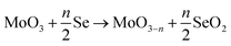 | (1) |
| |  | (2) |
The first reaction mainly occurs during the ramp-up temperature and the second reaction occurs in a constant temperature range, which is called the epitaxial process. The evolution of different morphologies in the CVD process depends upon various parameters such as the vapor pressure of precursors, reaction temperature, chemical potential, and distance between the precursors and substrate. The atomic ratio of Mo![[thin space (1/6-em)]](https://www.rsc.org/images/entities/char_2009.gif) :Se controls the final morphologies of the MoSe2 nanostructure. As reported in the literature,19,20 a large number of nucleation sites as MoO3−nSen are formed initially on the surface of the substrate, and thereafter the interfacial growth of MoSe2 nanostructure takes place and different morphologies evolve depending upon Mo:Se ratio. When the stoichiometric ratio of Mo and Se is 1:2, then the hexagonal shape is formed. Whereas, when the ratio of Mo:Se is greater than 1:2, the initially truncated triangles with Mo-terminated edges are formed and with rate limiting selenization snow-like structure is formed, as shown schematically in Fig. S1b–d of the ESI.† We examined the morphology of the prepared MoSe2 film using optical microscopy and atomic force microscopy (AFM) techniques. The optical images of the grown snow-like and hexagonal MoSe2 nanostructure films over the SiO2/Si substrate are shown in Fig. 1a and d, respectively. Fig. 1a clearly indicates the sharp edges formed in a snow-like structure, which are absent in hexagonal-shaped MoSe2. AFM studies also confirmed the same morphologies of the prepared MoSe2 film (Fig. 1b and e) and the height profile (Fig. 1c and f) study showed a thickness of around 2.4 and 2.3 nm for snow-like and hexagonal morphology, respectively. The thickness of the monolayer MoSe2 is around 0.7 nm based on crystallographic orientation,21 hence, the thickness of our film clearly indicates the formation of trilayer (3L) snow-like and hexagonal MoSe2 film. To examine the phase of the prepared MoSe2 film, we characterized it using Raman spectroscopy. Fig. 1g shows the Lorentzian fitted Raman spectra of snow-like and hexagonal 3L-MoSe2, indicating the presence of A1g mode around 240.9 and 240 cm−1, respectively, which represents out-of-plane plane vibrations of Se atoms in MoSe2. The broad and low intense peak at higher wavenumbers of 287.4 and 286.8 cm−1 is observed for snow-like and hexagonal, respectively, corresponding to the E12g mode associated with the in-plane vibrations of Mo and Se atoms.22 The presence of these peaks clearly indicates the formation of the 2H phase of MoSe2. Interestingly, an additional peak at ∼252.5 cm−1 was observed in snow-like nanostructure, which is usually associated with some kind of lattice disorder and/or Se vacancies by thermal annealing and hydrogen etching in the CVD process.23 Moreover, Raman mapping was performed to examine the distribution of defects in snow-like and hexagonal MoSe2, as shown in Fig. S2 of the ESI.† It clearly shows the uniform distribution of defects in snow-like MoSe2 and the absence of defects throughout the region in hexagonal MoSe2. Further, the semiconducting behaviour of the prepared film was examined using the PL spectroscopy technique. The Gaussian fitted room temperature PL spectra of the synthesized MoSe2 film are depicted in Fig. 1h, showing similar PL emissions for both morphologies. The exciton transition at the K-valley of the Brillouin zone of MoSe2 is the origin of the prominent peak for snow-like and hexagonal-shaped MoSe2 at approximately 1.57 and 1.58 eV, respectively.24 The strong PL emission clearly indicates the presence of direct bandgap in the prepared MoSe2 film, which can be suitable for optoelectronic applications.
:Se controls the final morphologies of the MoSe2 nanostructure. As reported in the literature,19,20 a large number of nucleation sites as MoO3−nSen are formed initially on the surface of the substrate, and thereafter the interfacial growth of MoSe2 nanostructure takes place and different morphologies evolve depending upon Mo:Se ratio. When the stoichiometric ratio of Mo and Se is 1:2, then the hexagonal shape is formed. Whereas, when the ratio of Mo:Se is greater than 1:2, the initially truncated triangles with Mo-terminated edges are formed and with rate limiting selenization snow-like structure is formed, as shown schematically in Fig. S1b–d of the ESI.† We examined the morphology of the prepared MoSe2 film using optical microscopy and atomic force microscopy (AFM) techniques. The optical images of the grown snow-like and hexagonal MoSe2 nanostructure films over the SiO2/Si substrate are shown in Fig. 1a and d, respectively. Fig. 1a clearly indicates the sharp edges formed in a snow-like structure, which are absent in hexagonal-shaped MoSe2. AFM studies also confirmed the same morphologies of the prepared MoSe2 film (Fig. 1b and e) and the height profile (Fig. 1c and f) study showed a thickness of around 2.4 and 2.3 nm for snow-like and hexagonal morphology, respectively. The thickness of the monolayer MoSe2 is around 0.7 nm based on crystallographic orientation,21 hence, the thickness of our film clearly indicates the formation of trilayer (3L) snow-like and hexagonal MoSe2 film. To examine the phase of the prepared MoSe2 film, we characterized it using Raman spectroscopy. Fig. 1g shows the Lorentzian fitted Raman spectra of snow-like and hexagonal 3L-MoSe2, indicating the presence of A1g mode around 240.9 and 240 cm−1, respectively, which represents out-of-plane plane vibrations of Se atoms in MoSe2. The broad and low intense peak at higher wavenumbers of 287.4 and 286.8 cm−1 is observed for snow-like and hexagonal, respectively, corresponding to the E12g mode associated with the in-plane vibrations of Mo and Se atoms.22 The presence of these peaks clearly indicates the formation of the 2H phase of MoSe2. Interestingly, an additional peak at ∼252.5 cm−1 was observed in snow-like nanostructure, which is usually associated with some kind of lattice disorder and/or Se vacancies by thermal annealing and hydrogen etching in the CVD process.23 Moreover, Raman mapping was performed to examine the distribution of defects in snow-like and hexagonal MoSe2, as shown in Fig. S2 of the ESI.† It clearly shows the uniform distribution of defects in snow-like MoSe2 and the absence of defects throughout the region in hexagonal MoSe2. Further, the semiconducting behaviour of the prepared film was examined using the PL spectroscopy technique. The Gaussian fitted room temperature PL spectra of the synthesized MoSe2 film are depicted in Fig. 1h, showing similar PL emissions for both morphologies. The exciton transition at the K-valley of the Brillouin zone of MoSe2 is the origin of the prominent peak for snow-like and hexagonal-shaped MoSe2 at approximately 1.57 and 1.58 eV, respectively.24 The strong PL emission clearly indicates the presence of direct bandgap in the prepared MoSe2 film, which can be suitable for optoelectronic applications.
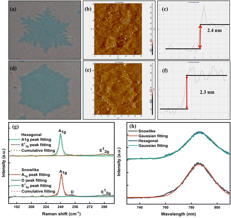 |
| | Fig. 1 (a and d) Optical images, (b and e) AFM images, and (c and f) corresponding height profiles of snow-like and hexagonal MoSe2 grown over SiO2/Si substrate; (g) room temperature Raman spectra (Lorentzian fitting of A1g mode); and (h) PL spectra for snow-like and hexagonal MoSe2. | |
Density functional study
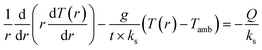
Since the synthesized film of MoSe2 consists of three layers, hence we have performed the density functional theory (DFT) calculations to obtain the electronic band structure and theoretically estimate the band gap of 3L-MoSe2 at 0 K, which can be confirmed experimentally by the temperature-dependent PL study of the prepared MoSe2 film. The lattice structure of MoSe2 contains one Mo atom sandwiched between two chalcogen atoms as shown in Fig. 2a, representing the top and side view of MoSe2, while Fig. 2b shows the unit cell of MoSe2. Successive layers are stacked one by one in such a way that the Mo atom is lined up with the Se atom of the next layer to generate a multilayer system and these layers interact via weak van der Waals forces. We used a 12 × 12 × 1 Monkhorst–Pack of K-points grids with path Γ–M–K–Γ of high symmetry points in the Brillouin zone for electronic band structure calculations. Fig. 2c and d show the electronic band structure and density of states, respectively, for 3L-MoSe2. We observed the lowest indirect bandgap of ∼0.98 eV for 3L-MoSe2, which matches well with the literature.25,26 The spin–orbit coupling effect shows a significant effect on the band structure and structural symmetry of a particular system. The energy levels at the K-point of the valence band and the Λ-point of the conduction band are corresponding to dx2–y2 and dxy orbitals of Mo atoms where the effect of spin–orbit coupling is very significant as compared to the energy levels corresponding to dz2 orbitals at Γ-point of the valence band and K-point of the conduction band. Fig. 2d shows the density of states (DOS) versus energy plot indicating the bandgap of 0.98 eV between the conduction band and valence band, which are generated by the hybridization of Mo-4d and Se-4p orbitals.
 |
| | Fig. 2 (a) Top and side view of 3L-MoSe2; (b) the 2D first BZ with high-symmetry points; (c) electronic band structure and (d) density of states for 3L-MoSe2. | |
The spin–orbit coupling leads to the splitting of the valence band at the K-point resulting in the formation of high energy (EH) and low energy (EL) excitons. It was theoretically demonstrated in the literature for molybdenum-based TMDCs that the energy separation between splitting energy levels at K-point is always positive, resulting in the low energy excitons (EL) as bright and high energy excitons (EH) as dark ones.27 Our theoretically calculated electronic band structure for 3L-MoSe2 shows the energy separation between dark and bright exciton around 0.184 eV due to the spin–orbit coupling. The interlayer coupling breaks the degeneracy of the energy level at the K-point. In 3L-MoSe2, the combination of interlayer and spin–orbit couplings results in the splitting of valence and conduction bands at the K-point because of the absence of inversion symmetry, as shown in Fig. S3 of ESI.†
Temperature-dependent PL study
To understand the thermal sensitive exciton behaviour of the prepared semiconducting MoSe2 film, we performed a temperature-dependent PL study in the temperature range 93–300 K for both morphologies (snow-like and hexagonal) of MoSe2. Fig. 3a and d show the Gaussian-fitted PL spectra for snow-like and hexagonal-shaped MoSe2 films, respectively at different temperatures. The room temperature PL spectra for both morphologies indicate the existence of high energy excitons (EH), which are blue-shifted at lower temperatures. The intensity of high-energy excitons increases at lower temperatures due to reduced non-radiative transitions via electron–phonon and phonon–phonon scatterings for both morphologies of MoSe2. Interestingly, we observed an additional feature when the surrounding temperature of MoSe2 film reached down to 213 K, a weak low-energy exciton peak (EL) appeared at lower energy for both morphologies. As per literature reports, the defect-bound excitons are the origin of this low-energy exciton peak at low temperatures.28 This low-energy exciton also follows the same trend as a high-energy exciton, i.e., it is blue-shifted and its intensity increases at lower temperatures, as observed in Fig. 3a and d. The binding energy of the defect-bound excitons for the prepared MoSe2 film was found to be 31–33 meV, lower than the high energy exciton at low temperatures, as suggested in the literature.29 Moreover, it was found that when the temperature was lowered to 123 K, the proportional intensities of EH and EL are in contrast for the snow-like and hexagonal MoSe2 films. It clearly showed that the defect-bound excitons (EL) are more dominant in snow-like MoSe2 compared to those in hexagonal MoSe2, which can be attributed to the presence of additional Se vacancies as defects in a snow-like MoSe2 film. The presence of defect has been confirmed by the Raman study, where we observed an additional D peak (at 252.5 cm−1) due to defects besides the A1g peak for snow-like MoSe2. The temperature-dependent PL study clearly suggests that emission phenomena in MoSe2 nanostructures can be tuned by changing morphologies, which can be used for developing desired atomically thin spintronic and valleytronic devices.
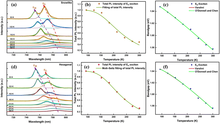 |
| | Fig. 3 Gaussian fitted PL spectra in the temperature range 93–300 K for (a) snow-like and (d) hexagonal MoSe2; variation of total PL intensity for EH exciton with temperature (b) snow-like and (e) hexagonal MoSe2; and fitting of variation in bandgap with temperature for (c) snow-like and (f) hexagonal MoSe2 film. | |
The electron undergoes the transition from an excited state of the recombination centre to the ground state via direct or indirect routes. At higher temperatures, radiative transitions are gradually replaced by non-radiative ones comprising the same defects, resulting in PL quenching as suggested by Mott–Seitz model.30,31 The temperature dependence of PL intensity of the MoSe2 film is shown in Fig. 3b and e and can be expressed as follows-
| |  | (3) |
where
I(
T) is the PL intensity at a given temperature
T,
A is known as a ratio of the nonradiative to radiative transitions probability,
Ea is the activation energy for nonradiative recombination and
kB is the Boltzmann constant. The configuration coordinate diagram is provided in Fig. S4 of the ESI,
† which comprises thermally induced excitation of the defect to the level at which adiabatic potentials of its ground and excited states cross, followed by nonradiative transition leading to phonon emission. The energy separation between the potential minimum of the excited state and the cross-over point of the excited and ground states provides the activation energy (
Ea). The obtained values of
A and
Ea for snow-like and hexagonal MoSe
2 are summarized in
Table 1. The lattice expansion along with increased phonon–phonon and electron–phonon interactions leads to the reduced intensity and red shifting of PL peaks with increasing temperature. The red-shift of
EH excitons with temperature for prepared snow-like and hexagonal MoSe
2 on SiO
2/Si substrate is shown in
Fig. 3c and f, respectively. This behaviour follows the Varshni and the O'Donnell and Chen models.
32,33 The modified Varshni equation can be expressed as follows-
| |  | (4) |
where
Eg(
T) and
Eg(0) represent the energy of
EH exciton at temperature
T and 0 K, respectively. The
α and
β are Varshni coefficients related to the temperature-dependent dilation of lattice and electron–phonon interaction. The obtained values of
Eg(0) and Varshni coefficients of high energy exciton for snow-like and hexagonal MoSe
2 are given in
Table 1.
Table 1 Fitting parameters related to thermal response of high energy excitons (EH) for snow-like and hexagonal MoSe2
| Parameter |
Snow-like MoSe2 |
Hexagonal MoSe2 |
|
Mott–Seitz equation
|
|
E
a (meV) |
69.64 |
77.98 |
|
A
|
22.86 |
38.91 |
|
|
Varshni's equation
|
|
E
0 (eV) |
1.66 |
1.65 |
|
α (10−4 eV K−1) |
4.03 |
5.11 |
|
β (K) |
108.35 |
260.52 |
|
|
O'Donnell's equation
|
|
E
0 (eV) |
1.65 |
1.64 |
|
S
|
2.24 |
2.38 |
| 〈ħω〉 (meV) |
17.06 |
25.83 |
We further fit the variation of bandgap using an additional formula, known as the O'Donnell and Chen equation to obtain the electron–phonon coupling constant (S) and the average energy of the phonon 〈ħω〉. This equation can be expressed as follows-
| |  | (5) |
The obtained values of Eg(0), S, and ħω for snow-like and hexagonal MoSe2 are given in Table 1. Similar values of Eg(0) for both morphologies are obtained using eqn (4) and (5). The higher values of coupling constant ‘S’ and average phonon energy ‘〈ħω〉’ for hexagonal MoSe2 compared to snow-like MoSe2 show a greater extent of phonon interaction with EH exciton in hexagonal MoSe2. The enhanced phonon–exciton interaction and lattice expansion with increasing temperature led to the linear increase of full width at half maximum (FWHM) for EH exciton, as shown in Fig. S5 of the ESI.† In summary, the temperature-dependent PL study of MoSe2 clearly suggests that the low energy excitons are predominant in snow-like MoSe2 due to the presence of defects and the electron–phonon coupling is stronger in hexagonal MoSe2. This study also indicates the tunability of bandgap in MoSe2 with morphology and external physical stimuli-like temperature.
Thermal transport behaviour of MoSe2 nanostructures
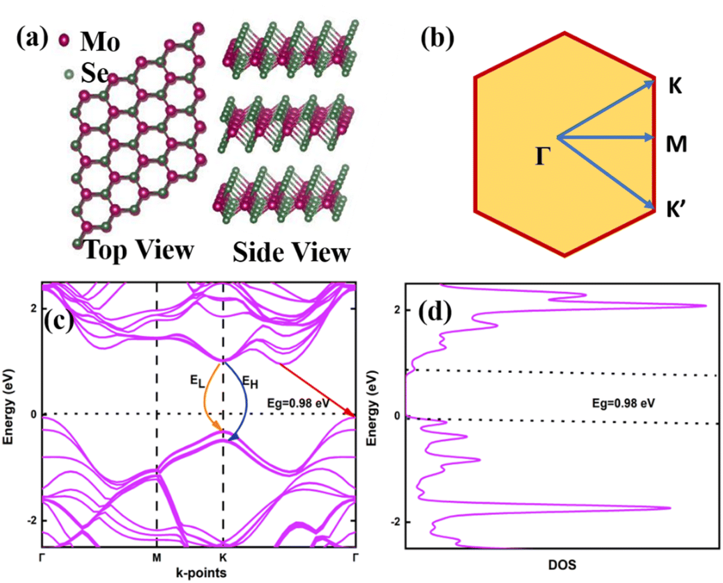
To evaluate the thermal conductivity and interfacial thermal conductance of snow-like and hexagonal MoSe2 thin film on a SiO2/Si substrate, we performed the optothermal Raman technique, which includes temperature and laser power-dependent Raman studies.17,33 In a temperature-dependent Raman study, the Raman shift is utilized to inspect the electron–phonon and phonon–phonon interactions. The temperature-dependent Raman study was performed using the LWD 50× objective lens in the temperature range 93–300 K. The temperature-dependent Raman spectra for snow-like and hexagonal MoSe2 films over the SiO2/Si substrate at different temperatures are shown in Fig. 4a and c, respectively. The remaining Lorentzian-fitted Raman spectra at other temperatures are provided in Fig. S6 of the ESI.† The corresponding variations in the peak position of A1g modes for both morphologies of the MoSe2 film with temperature are shown in Fig. 4b and d. Their linear and non-linear responses are analyzed using the following eqn (6) and (7). The linear dependence can be expressed as follows-where ω(T) and ω0 are the frequencies of the Raman mode at any temperature (T) and at 0 K, respectively, while slope χT is the first-order thermal coefficient. The corresponding χT values for snow-like and hexagonal MoSe2 are found to be −(0.0096 ± 0.0004) and −(0.0115 ± 0.0002) cm−1 K−1, respectively. The thermal response of A1g mode for snow-like MoSe2 is found non-linear, while for hexagonal MoSe2 it is found to be more linear in nature.
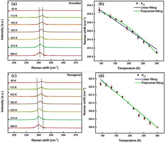 |
| | Fig. 4 Temperature-dependent Raman spectra of (a) snow-like and (c) hexagonal MoSe2; Raman shifts with temperature in (b) snow-like and (d) hexagonal MoSe2 using LWD 50× objective lens. | |
The non-linear thermal response of snow-like MoSe2 obeys the following second-order polynomial function, consisting of first- and second-order thermal coefficients (χ1, χ2).34
| | | ω(T) = ω0 + χ1T + χ2T2 | (7) |
The polynomial fit is found better for snow-like MoSe2 suggesting that the anharmonic effect of phonon–phonon coupling is the main cause of the nonlinear thermal response of Raman mode in snow-like MoSe2. The nonlinear thermal response of MoSe2 can be quantitatively evaluated using a semi-quantitative model by taking two effects into account. The first effect is the pure volume effect arising from the lattice thermal expansion and the second effect is the pure temperature effect resulting from three- and four-phonon scattering processes in phonon–phonon interaction. This semi-quantitative model can be expressed as follows-35,36
where Δ
ωE and Δ
ωA denote the Raman shifts arising from pure volume and pure temperature effects, respectively. The effect of volume expansion on Raman shift can be explained by the following Gruneisen constant model.
35,36| |  | (9) |
where
n is the degeneracy, and its value in the A
1g mode for MoSe
2 is 1. The thermal expansion coefficient of the materials is denoted by
αT, while
γ is the Gruneisen parameter. The integral shows the decrease in vibration frequency with volume expansion. The value of
ω0 is found by linear fitting. Additionally, the product
γαT of the MoSe
2 nanostructure is given in the form of the following polynomial expression.
35,36where
a,
b, and
c are the fitting constants. The anharmonic impact of three- and four-phonon scattering processes is the primary cause of the pure temperature effect comprising different light–matter interactions such as photon absorption, emission, and scattering. The semiquantitative model, developed by Klemens, expresses the pure temperature effect as follows-
37| |  | (11) |
where,
is the Boltzmann constant,
T is the temperature (in kelvin), while coefficients
A and
B denote the separate contributions of the three- and four-phonon processes, respectively.
The nonlinear temperature dependency of Raman shifts is then fitted using eqn (8)–(11) as was done in our recent study on MoS2.38 The contributions from the processes of thermal expansion, three-phonon, and four-phonon scatterings for both the morphologies of MoSe2 are shown in Fig. 5. The A and B fit parameters can be extracted by nonlinear temperature response. The retrieved fitting parameters are A = 0.38357, B = −0.0405 for snow-like MoSe2 and A = −0.66297, B = 0.00289 for the hexagonal MoSe2 film. Here, γ = 0.2 as the Gruneisen parameter and thermal expansion coefficient αT = 10.5 × 10⁻⁵ K−1 are taken for A1g mode of MoSe2 from literature.39,40 In Fig. 5, the observed experimental data are displayed along with the predicted temperature-dependent phonon profiles, i.e., contributions of thermal expansion, three- and four-phonon scattering processes for the A1g mode of snow-like (Fig. 5a), and hexagonal (Fig. 5b) MoSe2 film. The non-linear temperature dependence of the Raman shift for snow-like MoSe2 can be explained by the four-phonon process at low temperatures, with thermal expansion mostly acting as a weak linear temperature-dependent component. This study clearly suggests that the anharmonic effect arising from the four-phonon process is the primary cause of the non-linear temperature dependency in snow-like MoSe2, while the three-phonon process is mainly responsible for the non-linear temperature response of hexagonal MoSe2. The CVD-grown MoSe2 film showed a higher degree of non-linearity in the Raman shift due to the presence of defects and chemically active sites. The probability of higher-order phonon scattering is increased as the defect increases. The four-phonon process is dominant in snow-like MoSe2 due to the additional presence of defects associated with Se vacancy. In summary, the shift in the Raman modes with temperature for both morphologies of 3L-MoSe2 film over the SiO2/Si substrate can be attributed to the thermal expansion of the crystal and the resulting anharmonicity of phonon modes. The shifts in phonon energies occur due to the lattice contraction or expansion with temperature variation resulting in the change of atomic mean positions and interatomic forces. Consequently, phonon shift with temperature can be utilized to observe local temperature evolution in the synthesized semiconducting MoSe2 film by measuring the change in A1g Raman mode. The linear increase of FWHM for the A1g mode with increasing temperature is shown in Fig. S6 of the ESI,† suggesting the softening of the mode in both morphologies of MoSe2. Hence, our study suggests that phonon confinement in the MoSe2 film is extremely sensitive to thermal energy, signifying its better thermal transport behaviour, which can play a vital role in MoSe2-based devices.
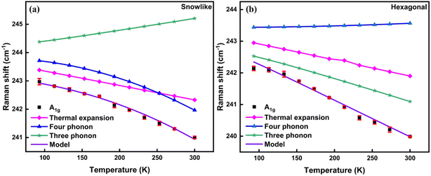 |
| | Fig. 5 The simulation of the temperature dependence of Raman shift considering the individual contributions from the processes of thermal expansion, three-phonon, and four-phonon scatterings for (a) snow-like; and (b) hexagonal MoSe2 film. | |
Power-dependent Raman study
In order to calculate the thermal conductivity of SiO2/Si substrate-supported snow-like and hexagonal 3L-MoSe2, we studied their phonon confinement behaviour in response to a local rise in temperature by laser heating with different laser powers. Raman spectra collected at different laser powers using the LWD 50× objective lens are shown in Fig. 6a and c for snow-like and hexagonal MoSe2, respectively, and the linear response of their corresponding Raman shifts with laser powers are shown in Fig. 6b and d, respectively. An enhancement in the intensity of the A1g mode due to increasing incident light intensity and red shift was observed with increasing laser power due to the softening of bonds via local temperature rise in MoSe2. Raman spectra at different laser power using a 100× objective lens are shown in Fig. S7 of the ESI.† The linear Raman shift in power-dependent Raman spectra can be described as follows-where P is incident laser power at the sample and the slope  is a first-order power-dependent coefficient. The χP values are found to be −(0.4797 ± 0.0150) and −(0.8307 ± 0.0801) cm−1 mW−1 for snow-like and hexagonal MoSe2, respectively, using LWD 50× lens and in the case of 100× lens χP values are −(0.4919 ± 0.0234) and −(1.2236 ± 0.1367) cm−1 mW−1 for snow-like and hexagonal MoSe2, respectively. In addition to the Raman shift with laser power, we also noticed the linear increase in FWHM with laser heating, as shown in Fig. S8 of the ESI.† The increase in FWHM and observed red shift in the A1g mode with increasing laser power can be directly ascribed to the lattice expansion and softening of bonds.
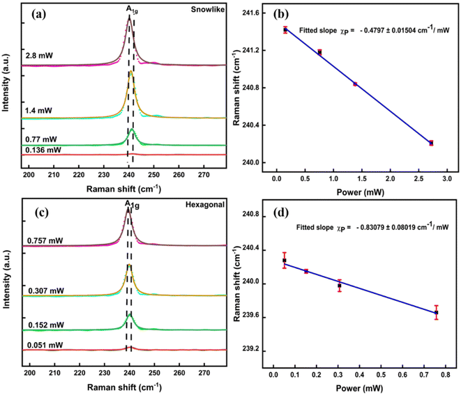 |
| | Fig. 6 Lorentzian fitted power-dependent Raman spectra for (a) snow-like and (c) hexagonal MoSe2 and (b and d) their corresponding Raman shifts with incident laser power, using the LWD 50× objective lens. | |
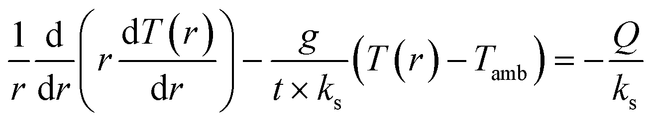
We have extracted the interfacial thermal conductance per unit area (g) and thermal conductivity (ks) of the synthesized MoSe2 film over the SiO2/Si substrate using the strategy from our earlier report on thermal conductivity of MoS2.33 Thermal conduction through MoSe2 film over the SiO2/Si substrate can be described by following heat diffusion eqn (13) in the form of cylindrical coordinate.41,42
| |  | (13) |
where
T(
r) is the radial temperature distribution,
Tamb is the global ambient temperature and
r is the distance measured from centre of the laser beam. Here,
t is the thickness of synthesized MoSe
2 film,
ks is the in-plane thermal conductivity of the SiO
2/Si supported MoSe
2 film,
g is the total interfacial thermal conductance per unit area between the film and the substrate, and
Q is the volumetric optical heating power density. This equation has been solved using our developed MATLAB simulation, as described in our earlier reports.
33,38 The solution provides an expression for
Rm depending on the ratio of
g and
ks, while two
Rm values are obtained by different laser spot sizes using two distinct objective lenses 100× and LWD 50× to obtain the final value of
g and
ks. We calculated the radius of the laser beam spot size for 100× and LWD 50× objective lenses to be around 0.19 and 0.28 μm, respectively, a detailed calculation is provided in Section S8 of the ESI.
† Experimentally the value of thermal resistance (
Rm) of the synthesized MoSe
2 film can be calculated
via the following relation-
| |  | (14) |
where, the absorption coefficient
αa ∼ 0.161 for trilayer MoSe
2, details calculation is provided in the Section S9 of the ESI.
† For the snow-like MoSe
2 film, we found the experimental value of
Rm = 3.8521 × 10
5 and 3.2886 × 10
5 KW
−1 for the spot size 0.19 μm (objective lens 100×) and 0.28 μm (objective lens LWD 50×), respectively and for the hexagonal MoSe
2 film, the experimental value of
Rm = 6.6086 × 10
5 and 4.4871 × 10
5 KW
−1 for the spot size 0.19 and 0.28 μm, respectively. We determined the value of
g ∼ 6.0788 ± 1.3707 MW m
−2 K
−1 and
ks ∼ 36 ± 6 W m
−1 K
−1 for snow-like MoSe
2 and
g ∼ 3.2278 ± 0.58565 MW m
−2 K
−1 and
ks ∼ 41 ± 7 W m
−1 K
−1 for hexagonal MoSe
2, by solving the MATLAB simulation. The decrease in phonon group velocity induced by defects, as well as phonon localization at atomic-scale lattice defects results in lower thermal conductivity of snow-like MoSe
2 compared to the hexagonal MoSe
2. Additionally, the contribution of low-frequency phonons declines with increasing defects as a result of enhanced coupling between low-frequency and high-frequency phonons. The interfacial thermal conductance of the snow-like MoSe
2 film is found higher due to the presence of additional Se vacancy defects.
Table 2 summarizes the comparison of our findings on the optothermal Raman measurements for thermal conductivity of 3L-MoSe
2 with other reports on different 2D materials. It clearly shows that our prepared 3L-MoSe
2 on SiO
2/Si substrate shows significant thermal conductivity for both morphologies making them suitable for thermal transport in optoelectronic devices. The semiconducting response of such optoelectronic devices can be tuned by using different morphology of MoSe
2 and/or applying different temperatures.
Table 2 Thermal conductivity of 2D materials by the optothermal Raman method
| 2D materials |
Raman mode |
k
s (W m−1 K−1) |
Reference |
| 200 nm-graphene (supported SiO2/Si) |
G |
370 + 650/−320 |
41
|
| 4 nm-PtS2 (suspended) |
Eg |
85.6 ± 7.70 |
43
|
| 4.5 nm-PtSe2 (suspended) |
Eg |
40.4 ± 4.67 |
43
|
| 5 to 15L-SnSe2 (suspended) |
A1g |
1.80–2.90 |
44
|
| 2L-MoS2 (supported SiO2/Si) |
A1g |
42 ± 8 |
33
|
| 2L-MoS2 (supported Au–SiO2/Si) |
A1g |
35 ± 7 |
16
|
| 2L-MoSe2 (supported Au–SiO2/Si) |
A1g |
17 ± 4 |
16
|
| Snow-like 3L-MoSe2 (supported SiO2/Si) |
A1g |
36 ± 6 |
This work |
| Hexagonal 3L-MoSe2 (supported SiO2/Si) |
A1g |
41 ± 7 |
This work |
Conclusions
In conclusion, we synthesized two different morphologies (snow-like and hexagonal) of 3L-MoSe2 over SiO2/Si substrate via the CVD technique. We reported for the first time morphological dependent phonon confinement behaviour of MoSe2 at low temperatures, revealing that the defect-bound excitons (EL) are more dominant in snow-like MoSe2 compared to hexagonal MoSe2 due to the presence of additional defects in snow-like MoSe2 film. We also demonstrated morphological-dependent thermal transport properties of MoSe2 for the first time to the best of our knowledge. We observed that four phonon scattering process is dominant in snow-like MoSe2 for thermal transport in comparison to three phonon process in hexagonal MoSe2. We also observed the thermal conductivity (ks) ∼ 36 ± 6 W m−1 K−1 and interfacial thermal conductance (g) ∼ 6.0788 ± 1.3707 MW m−2 K−1 for snow-like MoSe2 film and ks ∼ 41 ± 7 W m−1 K−1 and g ∼ 3.2278 ± 0.5856 MW m−2 K−1 for hexagonal MoSe2 film. The higher-order phonon scattering in snow-like MoSe2 results in lower thermal conductivity and higher interfacial thermal conductance compared to hexagonal MoSe2. Our study paves the way for developing MoSe2 based externally modulated optoelectronic device by tuning its morphology.
Author contributions
Jay Deep Gupta was involved in the idea of the project, the synthesis of material, analysing data, and writing the manuscript. Priyanka Jangra was involved in the investigation of DFT calculation. Bishnu Pada Majee was involved in the optothermal study. Ashish Kumar Mishra was involved in the supervision and administration of the project, arrangement of resources, data analysis, review, and editing of the manuscript.
Conflicts of interest
The authors declare that they have no known competing financial interests or personal relationships that could have appeared to influence the work reported in this paper.
Acknowledgements
The authors thank IIT (BHU) and its Central Instrument Facility. JDG is thankful to the Ministry of Education, Govt. of India for the Prime Minister Research Fellowship (PMRF). AKM acknowledges the support of SERB, India (Grant No. CRG/2020/002186). The authors also thank Dr Abhishek Sanskrityayn for the discussion on the mathematical model.
References
- X. Song, Z. Guo, Q. Zhang, P. Zhou, W. Bao and D. W. Zhang, Small, 2017, 13, 1700098 CrossRef PubMed.
- Q. H. Wang, K. Kalantar-Zadeh, A. Kis, J. N. Coleman and M. S. Strano, Nat. Nanotechnol., 2012, 7, 699–712 CrossRef CAS PubMed.
- C. Chakraborty, N. Vamivakas and D. Englund, Nanophotonics, 2019, 8, 2017–2032 CrossRef.
- S. I. Azzam, K. Parto and G. Moody, Appl. Phys. Lett., 2021, 118, 240502 CrossRef CAS.
- Z. Shi, H. Zhang, K. Khan, R. Cao, K. Xu and H. Zhang, Nano Res., 2022, 15, 104–122 CrossRef CAS.
- H. Lee, J. Ahn, S. Im, J. Kim and W. Choi, Sci. Rep., 2018, 8, 1–7 Search PubMed.
- S. Sotgiu, T. Venanzi, F. Macheda, E. Stellino, M. Ortolani, P. Postorino and L. Baldassarre, Phys. Rev. B, 2022, 106, 085204 CrossRef CAS.
- N. Kumar, J. He, D. He, Y. Wang and H. Zhao, Nanoscale, 2014, 6, 12690–12695 RSC.
- X. Wang, Y. Gong, G. Shi, W. L. Chow, K. Keyshar, G. Ye, R. Vajtai, J. Lou, Z. Liu, E. Ringe, B. K. Tay and P. M. Ajayan, ACS Nano, 2014, 8, 5125–5131 CrossRef CAS PubMed.
- S. Ren, Q. Tan and J. Zhang, J. Semicond., 2019, 40, 071903 CrossRef CAS.
- Y. Liu, Y. Liu, H. Zhou, Z. Yang, Y. Qu, Y. Tan and F. Chen, ACS Nano, 2021, 15, 16572–16580 CrossRef CAS PubMed.
- D. Saleta Reig, S. Varghese, R. Farris, A. Block, J. D. Mehew, O. Hellman, P. Woźniak, M. Sledzinska, A. el Sachat, E. Chávez-Ángel, S. O. Valenzuela, N. F. Van Hulst, P. Ordejón, Z. Zanolli, C. M. Sotomayor Torres, M. J. Verstraete and K. J. Tielrooij, Adv. Mater., 2022, 34, 2108352 CrossRef CAS PubMed.
- A. Kandemir, H. Yapicioglu, A. Kinaci, T. Çağin and C. Sevik, Nanotechnology, 2016, 27, 055703 CrossRef PubMed.
- Y. Hong, J. Zhang and X. C. Zeng, J. Phys. Chem. C, 2016, 120, 26067–26075 CrossRef CAS.
- H. Zobeiri, R. Wang, T. Wang, H. Lin, C. Deng and X. Wang, Int. J. Heat Mass Transfer, 2019, 133, 1074–1085 CrossRef CAS.
- X. Zhang, D. Sun, Y. Li, G. H. Lee, X. Cui, D. Chenet, Y. You, T. F. Heinz and J. C. Hone, ACS Appl. Mater. Interfaces, 2015, 7, 25923–25929 CrossRef CAS PubMed.
- J. Sun, K. Dai, W. Xia, J. Chen, K. Jiang, Y. Li, J. Zhang, L. Zhu, L. Shang, Z. Hu and J. Chu, ACS Omega, 2021, 6, 30526–30533 CrossRef CAS PubMed.
- J. Li, W. Yan, Y. Lv, J. Leng, D. Zhang, C. O. Coileaín, C. P. Cullen, T. Stimpel-Lindner, G. S. Duesberg, J. Cho, M. Choi, B. S. Chun, Y. Zhao, C. Lv, S. K. Arora and H. C. Wu, RSC Adv., 2020, 10, 1580–1587 RSC.
- J. Wang, X. Cai, R. Shi, Z. Wu, W. Wang, G. Long, Y. Tang, N. Cai, W. Ouyang, P. Geng, B. N. Chandrashekar, A. Amini, N. Wang and C. Cheng, ACS Nano, 2018, 12, 635–643 CrossRef CAS PubMed.
- W. Zheng, Y. Qiu, W. Feng, J. Chen, H. Yang, S. Wu, D. Jia, Y. Zhou and P. Hu, Nanotechnology, 2017, 28, 395601 CrossRef PubMed.
- M. Cowie, R. Plougmann, Y. Benkirane, L. Schué, Z. Schumacher and P. Grütter, Nanotechnology, 2022, 33, 125706 CrossRef PubMed.
- Z. Gan, E. Najafidehaghani, S. H. Han, S. Shradha, F. Abtahi, C. Neumann, J. Picker, T. Vogl, U. Hübner, F. Eilenberger, A. George and A. Turchanin, Small Methods, 2022, 6, 2200300 CrossRef CAS PubMed.
- M. Mahjouri-Samani, L. Liang, A. Oyedele, Y. S. Kim, M. Tian, N. Cross, K. Wang, M. W. Lin, A. Boulesbaa, C. M. Rouleau, A. A. Puretzky, K. Xiao, M. Yoon, G. Eres, G. Duscher, B. G. Sumpter and D. B. Geohegan, Nano Lett., 2016, 16, 5213–5220 CrossRef CAS PubMed.
- J. Xia, X. Huang, L. Z. Liu, M. Wang, L. Wang, B. Huang, D. D. Zhu, J. J. Li, C. Z. Gu and X. M. Meng, Nanoscale, 2014, 6, 8949–8955 RSC.
- S. Tongay, J. Zhou, C. Ataca, K. Lo, T. S. Matthews, J. Li, J. C. Grossman and J. Wu, Nano Lett., 2012, 12, 5576–5580 CrossRef CAS PubMed.
- Y. Sun, D. Wang and Z. Shuai, J. Phys. Chem. C, 2016, 120, 21866–21870 CrossRef CAS.
- L. Xu, L. Zhao, Y. Wang, M. Zou, Q. Zhang and A. Cao, Nano Res., 2019, 12, 1619–1624 CrossRef CAS.
- T. Godde, D. Schmidt, J. Schmutzler, M. Aßmann, J. Debus, F. Withers, E. M. Alexeev, O. del Pozo-Zamudio, O. V. Skrypka, K. S. Novoselov, M. Bayer and A. I. Tartakovskii, Phys. Rev. B, 2016, 94, 165301 CrossRef.
- M. A. Reshchikov, J. Appl. Phys., 2014, 115, 012010 CrossRef.
- N.F. Mott, Proc. R. Soc. London, Ser. A, 1938, 167, 384–391 Search PubMed.
- F. Seitz, Trans. Faraday Soc., 1939, 35, 74–85 RSC.
- K. P. O'Donnell and X. Chen, Appl. Phys. Lett., 1991, 58, 2924–2926 CrossRef.
- B. P. Majee, J. D. Gupta, A. Sanskrityayn and A. K. Mishra, J. Phys. Chem. C, 2021, 125, 14865–14873 CrossRef CAS.
- Z. Lin, W. Liu, S. Tian, K. Zhu, Y. Huang and Y. Yang, Sci. Rep., 2021, 11, 1–9 CrossRef PubMed.
- S. Najmaei, P. M. Ajayan and J. Lou, Nanoscale, 2013, 5, 9758–9763 RSC.
- X. T. Huang, Y. Gao, T. Q. Yang, W. C. Ren, H. M. Cheng and T. S. Lai, Sci. Rep., 2016, 6, 32236 CrossRef CAS PubMed.
- P. G. Klemens, Phys. Rev., 1966, 148, 845 CrossRef CAS.
- A. Singh, B. P. Majee, J. D. Gupta and A. K. Mishra, J. Phys. Chem. C, 2023, 127, 3787–3799 CrossRef CAS.
- D. J. Late, S. N. Shirodkar, U. V. Waghmare, V. P. Dravid and C. N. R. Rao, ChemPhysChem, 2014, 15, 1592–1598 CrossRef CAS PubMed.
- D. Kumar, V. Kumar, R. Kumar, M. Kumar and P. Kumar, Phys. Rev. B, 2022, 105, 085419 CrossRef CAS.
- W. Cai, A. L. Moore, Y. Zhu, X. Li, S. Chen, L. Shi and R. S. Ruoff, Nano Lett., 2010, 10, 1645–1651 CrossRef CAS PubMed.
- A. Mohapatra, S. Das, K. Majumdar, M. R. Rao and M. Jaiswal, Nanoscale Adv., 2021, 3, 1708–1716 RSC.
- S. Yin, W. Zhang, C. Tan, L. Chen, J. Chen, G. Li, H. Zhang, Y. Zhang, W. Wang and L. Li, J. Phys. Chem. C, 2021, 125, 16129–16135 CrossRef CAS.
- B. Zou, Y. Zhou, X. Zhang, M. Zhang, K. Liu, M. Gong and H. Sun, ACS Appl. Nano Mater., 2020, 3, 10543–10550 CrossRef CAS.
Footnote |
| † Electronic supplementary information (ESI) available: Density functional studies, configurational coordinate diagram, FWHM of temperature-dependent PL, temperature-dependent Raman spectra, power-dependent Raman spectra, calculations of laser spot size at different objective lenses, calculation of αa value for trilayer MoSe2. See DOI: https://doi.org/10.1039/d3na00164d |
|
| This journal is © The Royal Society of Chemistry 2023 |
Click here to see how this site uses Cookies. View our privacy policy here. 
 Open Access Article
 This Open Access Article is licensed under a Creative Commons Attribution-Non Commercial 3.0 Unported Licence
 *
*


 is the Boltzmann constant, T is the temperature (in kelvin), while coefficients A and B denote the separate contributions of the three- and four-phonon processes, respectively.

 is a first-order power-dependent coefficient. The χP values are found to be −(0.4797 ± 0.0150) and −(0.8307 ± 0.0801) cm−1 mW−1 for snow-like and hexagonal MoSe2, respectively, using LWD 50× lens and in the case of 100× lens χP values are −(0.4919 ± 0.0234) and −(1.2236 ± 0.1367) cm−1 mW−1 for snow-like and hexagonal MoSe2, respectively. In addition to the Raman shift with laser power, we also noticed the linear increase in FWHM with laser heating, as shown in Fig. S8 of the ESI.† The increase in FWHM and observed red shift in the A1g mode with increasing laser power can be directly ascribed to the lattice expansion and softening of bonds.