
 Open Access Article
 This Open Access Article is licensed under a Creative Commons Attribution-Non Commercial 3.0 Unported Licence
First-principles investigation of interface phenomena in hafnium-based metal–insulator–metal diodes
Eleonora
Pavoni
 a,
Elaheh
Mohebbi
a,
Pierluigi
Stipa
a,
Luca
Pierantoni
a,
Davide
Mencarelli
a,
Mircea
Dragoman
b,
Martino
Aldrigo
*b and
Emiliano
Laudadio
*a
a,
Elaheh
Mohebbi
a,
Pierluigi
Stipa
a,
Luca
Pierantoni
a,
Davide
Mencarelli
a,
Mircea
Dragoman
b,
Martino
Aldrigo
*b and
Emiliano
Laudadio
*a
aMarche Polytechnic University, Via Brecce Bianche, 60131 Ancona, Italy. E-mail: e.laudadio@staff.univpm.it; e.mohebbi@stafff.univpm.it
bNational Institute for Research and Development in Microtechnologies, IMT-Bucharest, 077190 Voluntari (Ilfov), Romania. E-mail: martino.aldrigo@imt.ro
First published on 24th March 2023
Abstract
Metal–insulator–metal (MIM) diodes are very interesting in many different applications exploiting environment-friendly renewable energy solutions. Moreover, since the dimensions of such devices are at the nanoscale, the size and the characteristics of their constitutive elements can drastically influence their macroscale performance. As it could be difficult to describe in detail the physical phenomena occurring among materials in nanoscale systems, in this work first-principles calculations have been used to study the structural and electrical properties of three different hafnium oxide (HfO2)-MIM diodes. These devices have been simulated at the atomistic level by interposing 3 nm of HfO2 between drain and source electrodes made of gold and platinum, respectively. The monoclinic and orthorhombic polymorphs of HfO2 have been considered to model different types of MIM diodes, and the interface geometries have been optimized to compute the current–voltage characteristics, reflecting the tunneling mechanisms occurring in such devices. The calculation of the transmission pathways has also been carried out to investigate the effects of atomistic coordinates despite the use of the same material. The results demonstrate the role of the Miller indices of metals and the influence of the HfO2 polymorphs on the MIM properties. In this study, the importance of interface phenomena on the measurable properties of the proposed devices has been investigated in detail.
Introduction
Nowadays, radio frequency (RF) energy harvesting and wireless power transfer (WPT) are concrete possibilities to exploit environment-friendly renewable energy to supply low-power devices and components in Internet-of-Things (IoT) networks, among others. This includes the ability to use dedicated RF sources to remotely power wireless systems such as small dust sensors1 or implantable sensors,2 whereas for the RF energy harvesting approach, the ambient RF radiation is scavenged to supply the right amount of energy to battery-less electronic devices, without the need for continuous monitoring of their charging status. In both cases, a diode is always required to rectify the input RF signal to extract a useful DC output.Metal–insulator–metal (MIM) diodes work according to the principle of electron tunnelling through a thin insulator between two metals (ideally with different work functions3,4); as such, they can be used without any bias voltage, but with the requirement of maximizing the asymmetry and nonlinearity of the current–voltage dependence. Moreover, these diodes can be easily integrated with antennas to create the so-called rectennas.5 In this respect, they are today extremely attractive for high-frequency applications where typical semiconductor-based devices cannot operate.6 The reasons are various: for example, MIM diodes have the high potential to operate under zero-bias conditions, exhibit fast response times (in the order of few femtoseconds) and can be manufactured using low-cost additive technologies.7
The real advantage of MIM diodes relies on the achievement of cut-off frequencies in the THz range, but their capability of zero-bias rectification can also be highly beneficial for WPT and energy harvesting applications at RF frequencies8 and beyond, up to hundreds of GHz (or even more). However, due to their intrinsic tunnelling mechanism, they need a very thin insulator (few-nm-thick oxide or ferroelectric material) to guarantee electron tunnelling. The latter aspect could represent a bottleneck for the fabrication of reliable devices with repeatable performance. This means that nanoscale dimensions play a fundamental role and differences of even a few nanometres can lead to very different responses of identical MIM diodes. Moreover, a real understanding of the states of metals, in terms of three-dimensional coordinates and of Miller indices is also crucial to fabricate a valid device with the desired capabilities. This is true because the phenomena characterizing the electrical properties of nanoscale devices are strongly dependent on interface modelling: the transition identification of bonding characters at metal-oxide edges with dissimilar electronic structures on the two sides is a decisive step in understanding how they are coupled with interfacial structural and compositional variations.
The fast response of MIM diodes is a key point for many nanoelectronics applications; the tunneling phenomenon, which is crucial for achieving high performance in these devices, is extremely sensitive to the nanoscale structural and chemical qualities of interface regions. Dudek et al.9 used different growing techniques to prepare thin HfO2 films on TiN electrodes and they investigated the charge transport characteristics of HfO2 MIM. The impact of the metal electrode on the conduction mechanisms of HfO2 thin film-based MIM capacitors was investigated at different temperatures by El Kamel et al.;10 in particular, they calculated the barrier heights, at metal–HfO2 interfaces, by considering Al, Cr, and Au electrodes. Furthermore, the review by Mitrovic et al.11 presents an overview of MIM diodes focusing on a few crucial points, such as zero-bias responsivity, zero-bias dynamic resistance, and asymmetry. Among others, they consider HfO2 as a dielectric material, summarizing the electron affinity, band gap, and permittivity. Moreover, they investigated some typical metals used in MIMs (Ni, Al, Au, Cr, and Ti), their skin depths, and their work functions.
Keepng in mind the abovementioned issues, in this work, accurate first-principle simulations have been performed to provide an in-depth insight into interface phenomena occurring in MIM diodes. The aim is to demonstrate how an a-priori study based on advanced computational tools and optimization techniques can help predict the effective performance of such nanoscale devices, hence offering a powerful method to choose the right approach for the successive fabrication steps. In detail, three different MIM diodes based on hafnium oxide (HfO2) have been modelled from an atomistic point of view, and their electronic transport properties have been investigated at the atomistic level. The transmission functions have been evaluated by simulating an electric field in two directions, i.e., from the source (bottom electrode) to the drain (top electrode) and vice versa. Platinum and gold have been chosen as the source and drain, respectively, thanks to their low roughness and to their different work functions, necessary to increase the asymmetry and nonlinearity of MIM diodes, as explained before. Between the two electrodes, a 3 nm-thick HfO2 layer has been interposed. We stress here that low roughness is an essential prerequisite to avoid defects when performing the deposition of HfO2. More generally, HfO2-based thin films could be prepared by using various deposition techniques such as atomic layer deposition (ALD), which is the most common, chemical vapor deposition (CVD), chemical solution deposition (CSD), pulsed laser deposition (PLD), RF sputtering, and physical vapor deposition (PVD)12–14 Since Böscke et al.15 reported ferroelectricity in ALD deposited Si-doped HfO2 thin films, many other dopants, such as Y16,17 and Zr,18,19 have been used to induce the formation of orthorhombic crystals in HfO2. Indeed, while bulk HfO2 crystallizes in a monoclinic phase (m-phase; space group: P21/c), it is believed that the ferroelectric behaviour in doped HfO2 results from the formation of a non-centrosymmetric Pca21 orthorhombic phase induced by the dopant20 However, a ferroelectric orthorhombic phase could form also in undoped HfO2 by tuning the grain size, which can be controlled by thermal treatment and film thickness12 and can be obtained by tuning the ALD deposition temperature, and for decreased film thicknesses.19,21,22 We stress here that ALD techniques have the advantage of providing conformal and homogeneous surfaces apt for the tunnelling phenomenon.
With regard to the metals used as electrodes, gold and platinum can exhibit different Miller indices, generating different possible interaction patterns. In this respect, for this work two different Miller configurations have been chosen (100 and 110) for both metal types, since these are the most stable configurations able to generate interfaces.23,24
Moreover, HfO2 is known to adopt different polymorphs with different structural and electrical properties.18,25 To investigate the effects of polymorphs on device's properties, monoclinic P21/c (m) and orthorhombic Pca21 (o) phases of HfO2 have been considered (Fig. 1), since the first is the most stable structure and the second has an intrinsic ferroelectric behaviour.22 Finally, due to asymmetry of the o-HfO2 phase, two possible interfaces can be generated, depending on the deposition direction of the polymorph. From a technological point of view, for example in ALD techniques, ferroelectric films can be grown by using the corresponding precursors (i.e., Hf and Zr, Y, Si, etc.) on the substrate surface, followed by their oxidation to produce a homogeneous oxide. Hence, the proper engineering necessary to grow different polymorphs is made possible by a careful deposition of the precursors during the ALD cycles (which are typically performed at 200 °C).
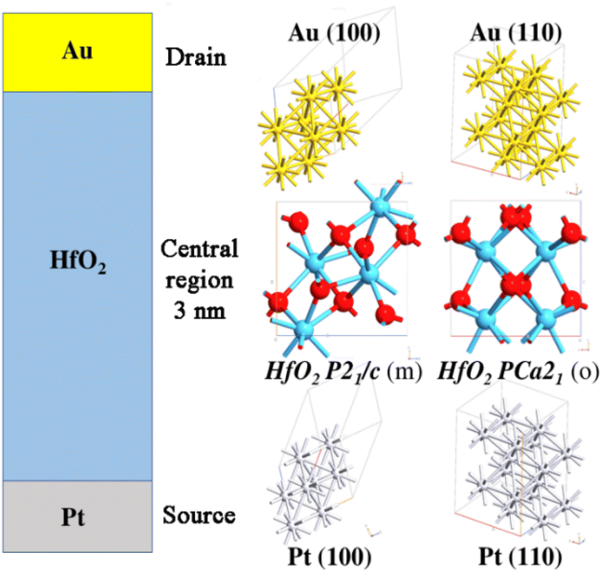 | ||
| Fig. 1 Schematic cross-section (left) and atomistic representation (right) of the studied MIM diodes, made of two different metals for the bottom (source) and top (drain) electrodes and of two different HfO2 polymorphs. | ||
To assess all the possible combinations involving Au and Pt Miller indices and HfO2 peculiarities, six HfO2-Au and six AfO2-Pt interfaces have been modelled. The optimization of the systems has been performed using density functional theory (DFT) with the generalized gradient approximation (GGA) based on the Perdew–Burke–Ernzerhof (PBE) exchange–correlation (xc) functional, together with norm-conserving PseudoDojo pseudopotentials to describe core electrons for each atom type. Considering the high number of d electrons involved in the chemical bonds on the interfaces, corrective Grimme D3 potentials have been added to DFT. This approach, called DFT-D3,26 offers the best trade-off between the accuracy degree and reasonable simulation time to detect interface phenomena. Finally, the most stable optimized interfaces have been used to model three MIM diodes and the GGA-PBE approach has been used again to calculate the current–voltage (I–V) characteristics, i.e., the first direct proof of the tunnelling behaviour of the studied devices.
Results and discussion
The search for the most stable interfaces is crucial to maximize the performance of MIM diodes and to avoid artifacts. For this reason, an extensive geometry optimization of the interfaces has been performed before the calculation of the I–V characteristics and the transmission pathways. As previously reported, both gold and platinum atomic systems have been considered with Miller indices equal to 100 and 110 in association with m-HfO2 and o-HfO2. Furthermore, because of the asymmetry of the orthorhombic unit cell, both lattice orientations have been included. By analysing the six interfaces with Au (100), stable and relaxed structures have been obtained in all cases, whereas the use of Au (110) led to distorted structures with the formation of electronic vacuum regions (Fig. 2). This was evident in the monoclinic form, whereas the asymmetry of the orthorhombic polymorph allowed more plausible interfaces although with certain intrinsic stress. Regarding the systems with Pt, a similar trend has been observed with respect to the Au interfaces, with more evident distortion in all models including Pt (110) (Fig. 3). An explanation of the larger interface deformation induced by Pt could be related to the stronger bonds formed by this metal with respect to those created by Au: gold completely fills the d orbitals involved in the chemical bonds with 10 d electrons, whereas Pt has 1 d electron less than gold. Both have the same number of orbitals; hence, the lack of one electron to complete the d orbitals in Pt leads to stronger chemical bonds.27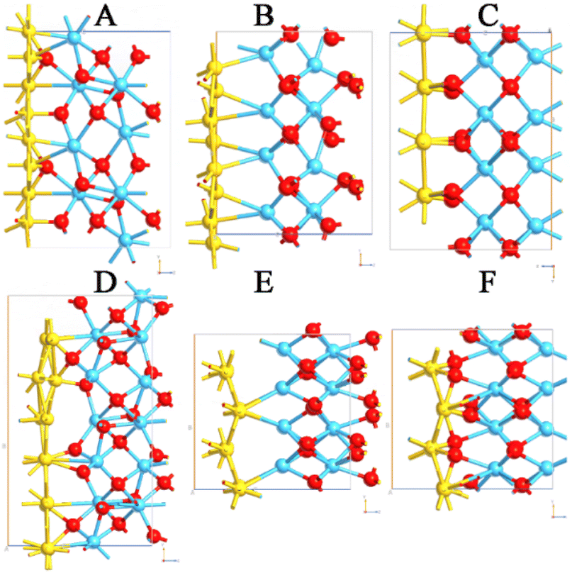 | ||
| Fig. 2 Optimized (A) Au (100)-P21/c, (B) Au (100) → Pca21, (C) Au (100) ← Pca21, (D) Au (110)-P21/c, (E) Au (110) → Pca21 and (F) Au (110) ← Pca21 (G) interfaces. The arrows indicate the direction of o-polarization. Au, Hf, and O entities are colored in yellow, grey, blue, and red, respectively. | ||
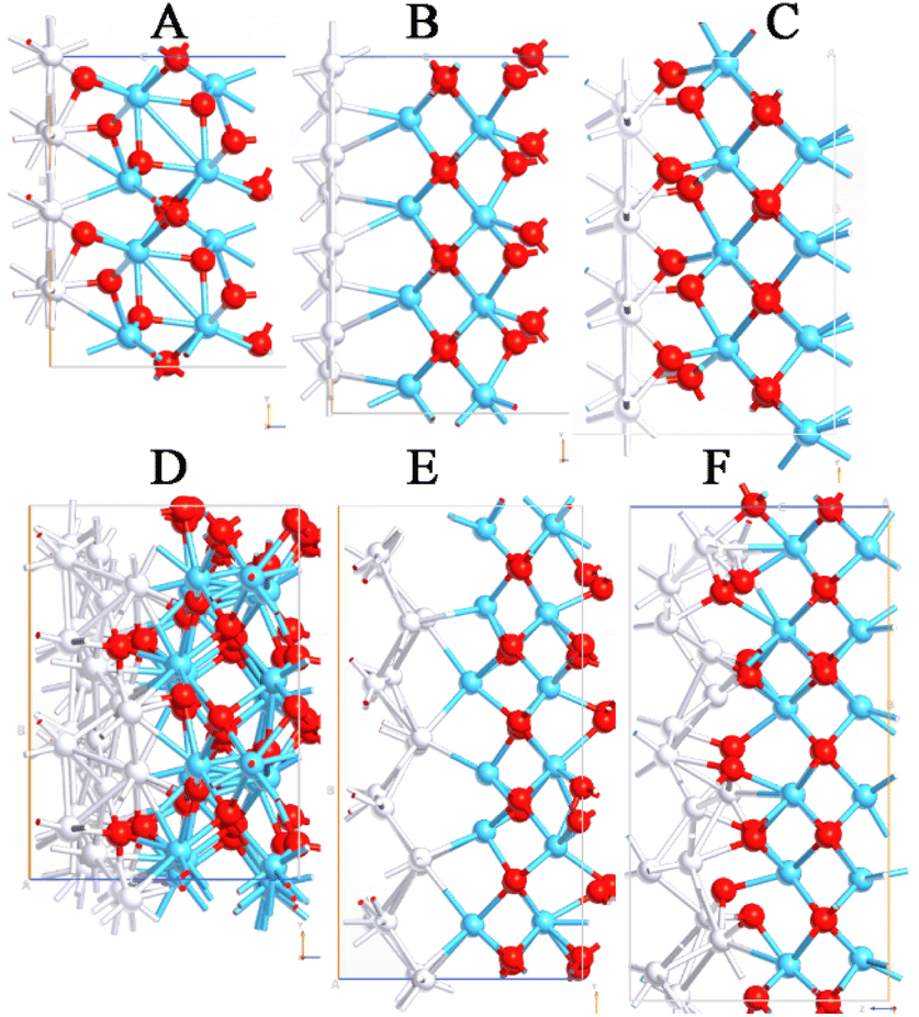 | ||
| Fig. 3 Optimized (A) Pt (100)-P21/c, (B) Pt (100) → Pca21, (C) Pt (100) ← Pca21, (D) Pt (110)-P21/c, (E) Pt (110) → Pca21, and (F) Pt (110) ← Pca21 interfaces. The arrows indicate the direction of o-polarization. Pt, Hf, and O entities are colored in yellow, grey, blue, and red, respectively. | ||
To verify the intrinsic stress of the interfaces, the cohesive formation energy values have been calculated (Table 1). The adhesion of Pt was about 0.2 eV stronger than that of Au, meaning that Pt resulted in being much more strongly bound to HfO2 with respect to Au. Moreover, since the o-HfO2 polymorphs may have two opposite orientations, it is worth noticing that the adhesion cohesive energy was −1.54 eV when Pt was directly bonded with O, and decreased to −1.12 eV when it was bound to Hf. A similar trend has been detected for Au interfaces, underlining the importance of short- and long-range phenomena between different materials. The detection of positive values of cohesive energy for different interfaces means that those interfaces are not possible, since they will be completely unstable and, from an experimental point of view, a separation between the materials should be expected. From a computational point of view, the cohesive energy has been calculated from electronic structure calculations and did not consider thermal and zero-point energy terms (i.e., vibrational contributions), but just considered optimizations in geometries. This means that by forcing the interfaces to stay together, we are sure about the reliability of the stable interfaces (i.e., those with 100 Miller indices), while those that are unstable (involving 110 orientation) have been completely discarded. For these reasons, only the most stable systems based on Au (100) and Pt (100) have been used to model three different MIM diodes. Each of them comprises 3 nm-thickness of HfO2 (i.e., one of the studied polymorphs).
| Interface with Au | Cohesive energy | Interface with Pt | Cohesive energy |
|---|---|---|---|
| (100)-P21/c HfO2 | −2.64 eV | (100)-P21/c HfO2 | −2.86 eV |
| (110)-P21/c HfO2 | 0.75 eV | (110)-P21/c HfO2 | 0.94 eV |
| (100) → Pca21 HfO2 | −0.93 eV | (100) → Pca21 HfO2 | −1.12 eV |
| (110) → Pca21 HfO2 | 0.03 eV | (110) → Pca21 HfO2 | 0.25 eV |
| (100) ← Pca21 HfO2 | −1.31 eV | (100) ← Pca21 HfO2 | −1.54 eV |
| (110) ← Pca21 HfO2 | −0.12 eV | (110) ← Pca21 HfO2 | 0.11 eV |
The thickness of the HfO2 thin film has been chosen to be equal to 3 nm for two main concatenated reasons: HfO2 acts as an insulator layer between two metallic electrodes but, to obtain a MIM architecture based on the quantum tunnelling effect, the HfO2 thickness should not be greater than 3–4 nm. Moreover, to model the MIM systems, a large enough portion of metals must be included on the right and on the left sides of the 3 nm-thick HfO2. Regions in the range of 1.84 nm for both Au and for Pt have been included following the optimized interfaces previously described. For the electrodes, we do not need to increase the dimensions more, since we use Dirichlet conditions for simulating gradient potentials, and this allows the effect of the electrodes to be simulated avoiding an increase in the explicit size of the system, thus maintaining high accuracy in the simulation results and decreasing the required computational time. For all these reasons, the dimensions of the modelled devices are as follows: x = 2.44 nm, y = 2.32 nm, and z = 6.68 nm for the m-MIM diode (Fig. 4A); x = 2.16 nm, y = 2.18 nm, and z = 6.32 nm for the “direct” o-MIM diode (i.e., polarization directed to the drain, Fig. 4B); x = 2.16 nm, y = 2.36 nm, and z = 6.32 nm for the “inverse” o-MIM diode (polarization directed to the source, Fig. 4C). In all cases, the geometry of the devices and their principle of operation did not show distortional phenomena when both metals were present, meaning that the generated interfaces were reliable and the modelled diodes are reasonable to translate the computational situation to the fabrication case. Moreover, no holes have been detected on the interfaces between the constitutive elements, meaning that the modelled atoms were correctly accommodated in the space and adopted their best coordination mode. Hence, the obtained configurations mimic very well the effective occurrences in the manufacturing process of multi-component systems.
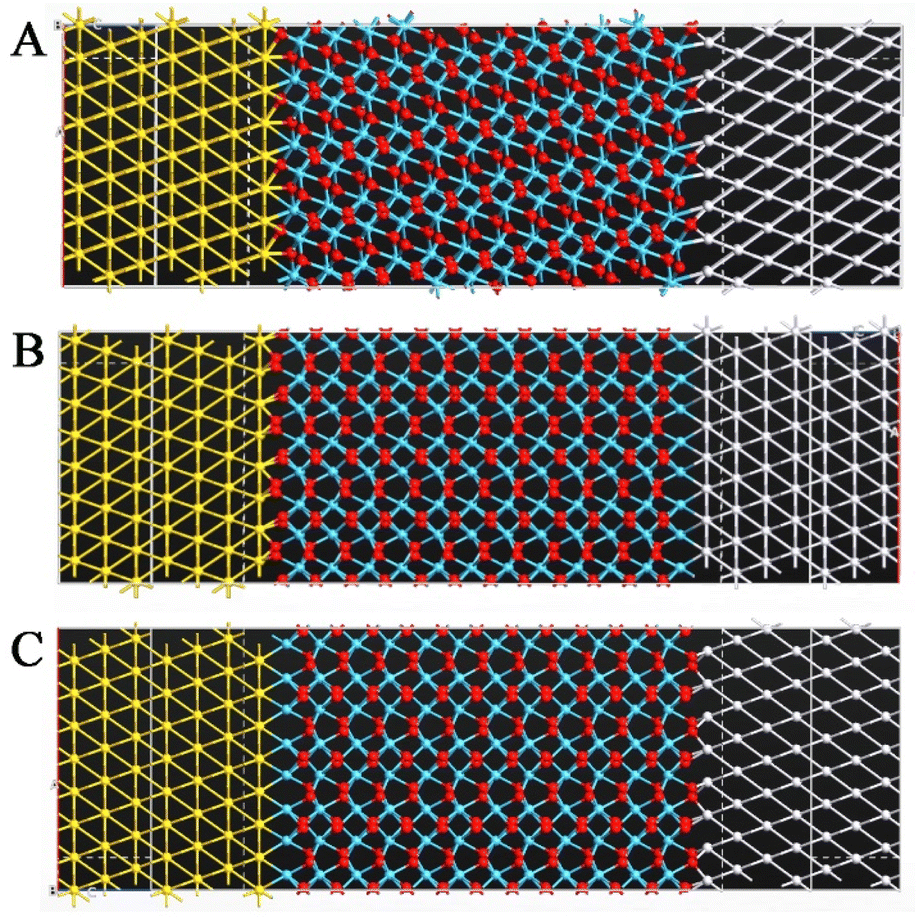 | ||
| Fig. 4 MIM diodes based on (A) m-HfO2, (B) o-HfO2 with polarization directed to the drain, and (C) o-HfO2 with polarization directed to the source. | ||
Before simulating the electronic transport properties, the calculation of the bandgap for m- and o-HfO2 polymorphs has been reported to quantify the effect of the thickness on the bandgap values. To show the differences, a comparison with bulk systems is provided in Table 2.
The I–V characteristics of the three systems have been computed following the previously described method, and the results have been shown and compared between them (Fig. 5A).
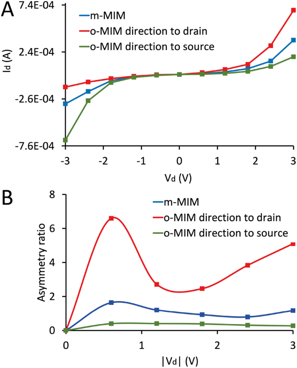 | ||
| Fig. 5 Calculated I–V characteristics (A) and the respective asymmetry ratios (B) of the three MIM diodes. | ||
For each simulation, 11 points have been considered in the whole voltage range between −3 and +3 V, since an increase in the number of points would make the simulations much heavier (in terms of memory occupation) and time consuming. In fact, the described computational method indicated together with the k-point sampling and the number of points to be written in the output requires about 14 days for each MIM diode configuration to obtain the presented simulation results.
While the monoclinic phase-based diode shows intermediate current values from negative to positive voltages, more evident differences have been observed in the I–V characteristics of the two systems containing the orthorhombic phase. Higher current values have been calculated for the system in which the spontaneous polarization of the orthorhombic phase is oriented towards the drain; on the contrary, lower values have been obtained when o-HfO2 is oriented towards the source. These results suggest how the exploitation of the ferroelectric phase of HfO2 could be beneficial for the optimization of MIM diode's performance for high-frequency detection and energy harvesting applications.
It is valuable to notice that an efficient rectification requires a large forward-to-backward current ratio. This ratio is referred to as the “asymmetry ratio” (AR) of the diode and some other figures of merit (such as the responsivity) also depend on the AR of the I–V behaviour. To analyze the AR of the I–V characteristics for different diodes, the ratio of the absolute value of current at positive (+V) and negative (−V) voltages has been considered by using the formula AR = |I(+V)/I(−V)|. The data obtained for the AR of the MIM diodes presented in Fig. 5A are shown in Fig. 5B. The results prove that the o-MIM to drain diodes attains the greatest AR value of 6.59 at a voltage |Vd| = 0.6 V, while m-MIM to drain and o-MIM to source diodes exhibit their maximum ARs of 1.63 and 0.4 at the same voltage, respectively. As one can see in Fig. 5B, the AR at higher voltages indicates lower values of the AR for voltage values in the range of 1.8–2.4 V, and the curves have increased the AR for voltage values greater than 2.4 V.28
We also stress here that the considered voltage range for the I–V curves have already been used in the literature for similar or even lower values of insulator's thickness (see, for example (ref. 29,30)). In any case, the corresponding maximum power is in the order of 1–2 mW, which does not create any issues in the experiments in terms of the breakdown of the measured devices.
To better understand the transport mechanisms of the three modelled MIM diodes, local current components have been investigated by extracting local transmission mechanisms at the atomic scale. Local charge transmissions are expressed as lines in the direction of the chemical bonds between the atoms, and these lines are referred to as the transmission pathways. The thickness and colour of these lines represent the magnitude of the local charge transmissions.
The pathways have been calculated for the devices under reverse bias (−3 V) and forward bias (+3 V). As expected, a linear trend has been observed for the MIM diode with the monoclinic HfO2 phase (Fig. 6A and B). This result is not surprising given the symmetric shape of the I–V curve: the current detected by applying a voltage between 0 V and +3 V has the same values (in terms of module) as the current recorded between 0 V and −3 V.
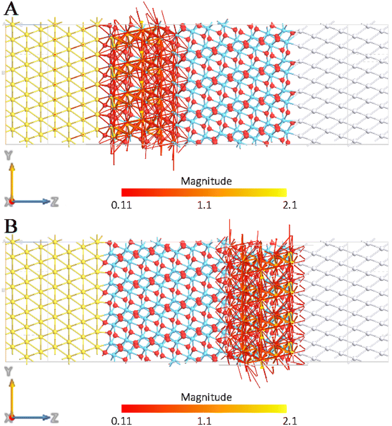 | ||
| Fig. 6 Transmission pathway plots for the MIM diode at a forward (A) and a reverse (B) bias voltage of 3 V calculated for P21/c HfO2. | ||
Thus, identical current values correspond to identical applied bias values (in terms of module), which shows the capability of this device to transport the current from platinum to gold and vice versa, despite the source and drain nature. From a chemical point of view, the symmetry of the monoclinic crystalline structure allows the electrons to move from the left to the right direction as well as the opposite one with the same magnitude. When the polarized Pca21 phase has been considered, some important peculiarities have been found. In the forward bias case (Fig. 7A), intense transmission pathways have been calculated allowing the forward conduction of current from the source to the drain. On the other hand, with the reverse bias case (Fig. 7B), an important decrease in the local transmission has been registered, confirming that the reverse conduction through the MIM diode is greatly suppressed in the presence of this orientation of the orthorhombic phase.
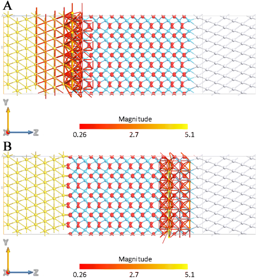 | ||
| Fig. 7 Transmission pathway plots for the MIM diode at a forward (A) and a reverse (B) bias voltage of 3 V calculated for Pca21 HfO2 oriented towards the drain. | ||
The opposite behaviour has been detected for the MIM diode in which the spontaneous polarization of the phase is oriented toward the source (Fig. 8), since the maximum transmission pathways have been calculated with the reverse bias.
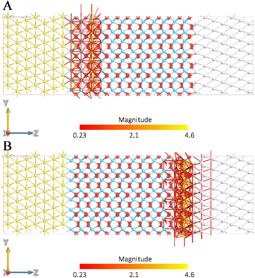 | ||
| Fig. 8 Transmission pathway plots for the MIM diode at a forward (A) and a reverse (B) bias voltage of 3 V calculated for Pca21 HfO2 oriented towards the source. | ||
Methods
All simulations have been performed using the DFT approach based on the Perdew–Burke–Ernzerhof (PBE)31 exchange–correlation (xc) functional with norm-conserving PseudoDojo32 pseudopotentials to describe core electrons for each atom type. The optimization of the interfaces has been computed using QuantumEspresso.33 The single particle wave-functions have been expanded into a basis of plane-wave (PW) functions, and D3 corrective terms34 have been added using periodic boundary conditions (PBCs) along all x and y axes. To simulate interface phenomena, periodicity along the z axis has been interrupted. The energy cut-off has been fixed at 1200 eV, and the Brillouin-zone integration was performed over a 15 × 15 × 15 k-point grid for the modelled interfaces. These parameters assure a total energy convergence of 5.0 × 10⁻⁶ eV per atom, a maximum stress of 2.0 × 10⁻² GPa, and a maximum displacement of 5.0 × 10⁻⁴ Å.The modern theory of polarization35 and the Berry phase operator method were used to obtain the polarization in the respective polymorphs. The total polarization is the sum of the electronic (Pe) and ionic (Pi) contributions. The electronic one (Pe) has been calculated as in eqn (1):
 | (1) |
The ionic contribution (Pi) has been calculated using a simple classical electrostatic sum of point charges, as reported in eqn (2):
 | (2) |
| Ec = Et − ΣxEt (x) | (3) |
The I–V characteristics and the transmission pathways have been calculated using the Quantum Atomistic Toolkit (Q-ATK) software package37 by maintaining the previously described first-principles approach, with the only differences related to the basis functions and the treatment boundary conditions (BCs). In this case, the single-electron eigenfunctions have been expanded into a set of finite-range atomic-like basis functions following the linear combination of atomic orbital (LCAO) representation. Then, the simulated I–V dependences have been referred to the specific transversal width of the modelled devices using periodic BCs along the x and y axes, whereas a fixed potential has been generated along the z-axis using Dirichlet conditions.38
In detail, PBCs have been used along the x and y axes, whereas a fixed potential has been generated along the z axis using Dirichlet conditions. Once the self-consistent non-equilibrium density matrix has been obtained, the electronic transport properties have been calculated using the nonequilibrium Green's function (NEGF) formalism. The device structures have been constructed as three regions, i.e., the source, central region, and drain (as it is displayed in Fig. 1), and coherent transport of electrons has been assumed to occur between source and drain contacts with Fermi levels μS and μD (and vice versa) through the central (HfO2) region. According to the Landauer formula, the coherent current between the electrodes is given by eqn (4):
 | (4) |
The transmission pathways have been calculated starting from the Landauer approach,39 which connects the external electrode current I(V) to the summed energy-dependent transmission probability T(E,V).40 With the aim to describe the variation of coherent electron transport through the system, local current components have been investigated at the atomistic level. Following the formalism in the ATK, the total transmission coefficient has been split into local bond contributions, Tij, which are represented by lines along the bond lengths, called transmission pathways. The relationship between the total transmission coefficient and the local bond contributions can be described by eqn (5):
 | (5) |
This approach suggests that a quantitative computationally inexpensive description of coherent transport in solid junctions is readily achievable, enabling new understanding and control of charge transport properties of atomistic–scale interfaces at large bias voltages.
Conclusions
In this paper, the modelling of MIM diodes has been presented focusing on interface phenomena among the various layers by the application of first-principles methods and also including the calculation of their electronic transport properties and their transmission pathways. The outcomes of this work demonstrate that both Au (100) and Pt (100) generate very stable interfaces with interposed HfO2. Moreover, the use of a monoclinic polymorph of the hafnium oxide system under study allows modelling a device able to transport the current from Au to Pt and vice versa, despite the source and drain nature. Finally, the devices with the orthorhombic ferroelectric phase have shown the highest and lowest current values when the orientation of the spontaneous polarization was toward the drain and the source, respectively. Altogether, the obtained results show the importance of investigating, at the atomistic scale, local phenomena at the interface level and the impact of different components on the measurable properties of the devices. The final outputs represent a powerful and promising approach for the preliminary study of such components in view of their successive fabrication, which can greatly benefit from the rigorous prediction of the best choice in terms of material type and growth method.Author contributions
Conceptualization, M. A. and E. M.; methodology, E. P., E. M., and E. L.; validation, E. P. and M. A.; investigation, E. P. and E. L.; data curation, E. M., P. S., D. M., and L. P.; writing—original draft preparation, E. L. and M. A.; writing—review and editing, P. S., D. M., L. P., and M. D.; visualization, M. D.; supervision, E. L. and M. A.; project administration, M. A., P. S., L. P., and D. M. All authors have read and agreed to the published version of the manuscript.Conflicts of interest
There are no conflicts to declare.Acknowledgements
This research was supported by the European Project H2020 FETPROACT- EIC-05-2019 “NANO-EH” under GA No. 951761, by two grants from the Romanian Ministry of Research, Innovation and Digitalization, CNCS-UEFISCDI, under Projects PN-III-P3-3.6-H2020-2020-0072 and PN-III-P4-PCE-2021-0223, within PNCDI III, and by the CINECA-HPC ISCRA MARCONI-100 computer system (Project No. HP10CMPMGP).References
- T. Salter, G. Metze and N. Goldsman, in 2009 IEEE Radio and Wireless Symposium, 2009, pp. 332–335 Search PubMed.
- S. Ladan and K. Wu, in 2013 IEEE MTT-S International Microwave Symposium Digest, MTT, 2013, pp. 1–4 Search PubMed.
- M. N. Gadalla, M. Abdel-Rahman and A. Shamim, Sci. Rep., 2014, 4, 4270 CrossRef CAS PubMed.
- S. Joshi and G. Moddel, IEEE J. Photovolt., 2016, 6, 668–672 Search PubMed.
- G. D. Boreman, Electron. Lett., 2004, 40(2), 116–118 CrossRef.
- S. Grover and G. Moddel, IEEE J. Photovolt., 2011, 1, 78–83 Search PubMed.
- M. Bareiß, B. Weiler, D. Kälblein, U. Zschieschang, H. Klauk, G. Scarpa, B. Fabel, P. Lugli and W. Porod, in 2012 IEEE Silicon Nanoelectronics Workshop, SNW, 2012, pp. 1–2 Search PubMed.
- J. G. Simmons, J. Appl. Phys., 1964, 35, 2472–2481 CrossRef.
- P. Dudek, R. Schmidt, M. Lukosius, G. Lupina, C. Wenger, A. Abrutis, M. Albert, K. Xu and A. Devi, Thin Solid Films, 2011, 519, 5796–5799 CrossRef CAS.
- F. el Kamel, P. Gonon, C. Vallée and C. Jorel, J. Appl. Phys., 2009, 106, 064508 CrossRef.
- I. Z. Mitrovic, S. Almalki, S. B. Tekin, N. Sedghi, P. R. Chalker and S. Hall, Materials, 2021, 14 Search PubMed.
- T. Mittmann, M. Materano, P. D. Lomenzo, M. H. Park, I. Stolichnov, M. Cavalieri, C. Zhou, C. C. Chung, J. L. Jones, T. Szyjka, M. Müller, A. Kersch, T. Mikolajick and U. Schroeder, Adv. Mater. Interfaces, 2019, 6, 1900042 CrossRef.
- E. P. Gusev, C. Cabral, M. Copel, C. D'Emic and M. Gribelyuk, Microelectron. Eng., 2003, 69, 145–151 CrossRef CAS.
- T. Shimizu and H. Funakubo, in Ferroelectricity in Doped Hafnium Oxide: Materials, Properties and Devices, ed. U. Schroeder, C. S. Hwang and H. Funakubo, Woodhead Publishing, 2019, pp. 173–192 Search PubMed.
- T. S. Böscke, J. Müller, D. Bräuhaus, U. Schröder and U. Böttger, Appl. Phys. Lett., 2011, 99, 102903 CrossRef.
- J. Müller, U. Schröder, T. S. Böscke, I. Müller, U. Böttger, L. Wilde, J. Sundqvist, M. Lemberger, P. Kücher, T. Mikolajick and L. Frey, J. Appl. Phys., 2011, 110, 114113 CrossRef.
- E. Pavoni, E. Mohebbi, D. Mencarelli, P. Stipa, E. Laudadio and L. Pierantoni, Nanomaterials, 2022, 12, 4324 CrossRef CAS PubMed.
- E. Pavoni, E. Mohebbi, P. Stipa, D. Mencarelli, L. Pierantoni and E. Laudadio, Materials, 2022, 15, 4175–4188 CrossRef CAS PubMed.
- J. Müller, T. S. Böscke, U. Schröder, S. Mueller, D. Bräuhaus, U. Böttger, L. Frey and T. Mikolajick, Nano Lett., 2012, 12, 4318–4323 CrossRef PubMed.
- R. Materlik, C. Künneth, M. Falkowski, T. Mikolajick and A. Kersch, J. Appl. Phys., 2018, 123, 12465–12546 CrossRef.
- K. D. Kim, M. H. Park, H. J. Kim, Y. J. Kim, T. Moon, Y. H. Lee, S. D. Hyun, T. Gwon and C. S. Hwang, J. Mater. Chem. C, 2016, 4, 6864–6872 RSC.
- P. Polakowski and J. Müller, Appl. Phys. Lett., 2015, 106, 232905 CrossRef.
- D. Su, S. Dou and G. Wang, NPG Asia Mater., 2015, 7, e155 CrossRef CAS.
- V. P. Santos and G. A. Camara, Results in Surfaces and Interfaces, 2021, 3, 100006 CrossRef.
- E. Laudadio, P. Stipa, L. Pierantoni and D. Mencarelli, Crystals, 2022, 12, 90 CrossRef CAS.
- S. Grimme, J. Antony, S. Ehrlich and H. Krieg, J. Chem. Phys., 2010, 132, 154104 CrossRef PubMed.
- Q. Cai, X. Wang and J. G. Wang, J. Phys. Chem. C, 2013, 117, 21331–21336 CrossRef CAS.
- Z. Zhu, S. Grover, K. Krueger and G. Moddel, 2011 37th IEEE Photovoltaic Specialists Conference, 2011, pp. 2120–2122 Search PubMed.
- A. Campera, G. Iannaccone and F. Crupi, IEEE Trans. Electron Devices, 2007, 54, 83–89 CrossRef CAS.
- K. Mistry, M. Yavuz and K. P. Musselman, J. Appl. Phys., 2017, 121, 184504 CrossRef.
- Z. Wan, Q.-D. Wang, D. Liu and J. Liang, Comput. Mater. Sci., 2021, 198, 110699 CrossRef CAS.
- M. J. van Setten, M. Giantomassi, E. Bousquet, M. J. Verstraete, D. R. Hamann, X. Gonze and G.-M. Rignanese, Comput. Phys. Commun., 2018, 226, 39–54 CrossRef CAS.
- P. Giannozzi, O. Andreussi, T. Brumme, O. Bunau, M. Buongiorno Nardelli, M. Calandra, R. Car, C. Cavazzoni, D. Ceresoli, M. Cococcioni, N. Colonna, I. Carnimeo, A. Dal Corso, S. de Gironcoli, P. Delugas, R. A. Distasio, A. Ferretti, A. Floris, G. Fratesi, G. Fugallo, R. Gebauer, U. Gerstmann, F. Giustino, T. Gorni, J. Jia, M. Kawamura, H. Y. Ko, A. Kokalj, E. Kücükbenli, M. Lazzeri, M. Marsili, N. Marzari, F. Mauri, N. L. Nguyen, H. v. Nguyen, A. Otero-De-La-Roza, L. Paulatto, S. Poncé, D. Rocca, R. Sabatini, B. Santra, M. Schlipf, A. P. Seitsonen, A. Smogunov, I. Timrov, T. Thonhauser, P. Umari, N. Vast, X. Wu and S. Baroni, J. Phys.: Condens. Matter, 2017, 29, 32 CrossRef PubMed.
- J. Witte, N. Mardirossian, J. B. Neaton and M. Head-Gordon, J. Chem. Theory Comput., 2017, 13, 2043–2052 CrossRef CAS PubMed.
- R. D. King-Smith and D. Vanderbilt, Phys. Rev. B: Condens. Matter Mater. Phys., 1993, 47, 1651 CrossRef CAS PubMed.
- S. T. Fan, Y. W. Chen and C. W. Liu, J. Phys. D: Appl. Phys., 2020, 53, 23LT01 CrossRef CAS.
- S. Smidstrup, T. Markussen, P. Vancraeyveld, J. Wellendorff, J. Schneider, T. Gunst, B. Verstichel, D. Stradi, P. A. Khomyakov, U. G. Vej-Hansen, M.-E. Lee, S. T. Chill, F. Rasmussen, G. Penazzi, F. Corsetti, A. Ojanperä, K. Jensen, M. L. N. Palsgaard, U. Martinez, A. Blom, M. Brandbyge and K. Stokbro, J. Phys.: Condens. Matter, 2019, 32, 015901 CrossRef PubMed.
- L. Gélébart, C. R. Mec., 2020, 348, 693–704 Search PubMed.
- R. Landauer, IBM J. Res. Dev., 1957, 1, 223–231 Search PubMed.
- G. C. Solomon, C. Herrmann, T. Hansen, V. Mujica and M. A. Ratner, Nat. Chem., 2010, 2, 223–228 CrossRef CAS PubMed.
| This journal is © The Royal Society of Chemistry 2023 |