DOI:
10.1039/D3NA00061C
(Paper)
Nanoscale Adv., 2023,
5, 1943-1955
Angle-resolved plasmonic photocapacitance of gold nanorod dimers†
Received
26th January 2023
, Accepted 17th February 2023
First published on 28th February 2023
Abstract
The assembly of nanostructures with plausible statistical orientations has provided the opportunity to correlate physical observables to develop a diverse range of niche applications. The dimeric configurations of gold nanorods have been chosen as atypical model systems to correlate optoelectronic with mechanical properties at a number of combinations of angular orientations. Metals are considered as conductors in electronics and reflectors in optics – therefore, metallic particles at the nanoscale exhibit unique optoelectronic characteristics that enable the design of materials to meet the demand of the modern world. Gold nanorods have often been adopted as prototypical anisotropic nanostructures owing to their excellent shape-selective plasmonic tunability in the vis-NIR region. When a pair of metallic nanostructures is sufficiently close to exhibit electromagnetic interaction, the evolution of collective plasmon modes, substantial enhancement of the near-field and strong squeezing of the electromagnetic energy at the interparticle spatial region of the dimeric nanostructures occur. The localised surface plasmon resonance energies of the nanostructured dimers strongly depend on the geometry as well as the relative configurations of the neighbouring particle pairs. Recent advances in the ‘tips and tricks’ guide have even made it possible to assemble anisotropic nanostructures in a colloidal dispersion. The optoelectronic characteristics of gold nanorod homodimers at different mutual orientations with statistical variation of the angle between 0 and 90° at particular interparticle distances have been elucidated from both theoretical and experimental perspectives. It has been observed that the optoelectronic properties are governed by mechanical aspects of the nanorods at different angular orientations of the dimers. Therefore, we have approached the design of an optoelectronic landscape through the correlation of the plasmonics and photocapacitance through the optical torque of gold nanorod dimers.
1. Introduction
The spatial organisation of plasmonic nanostructures results in unique optoelectronic properties governed by mechanical aspects. This enables the design of a growing number of materials for applications in the miniaturisation of modern nanoelectronic devices.1 The fabrication of highly energetic capacitors based on nanostructures is becoming crucial for electrical energy storage because of their significant burst power and enhanced storage capability.2,3 The harvesting of electromagnetic energy in free space results in uses in a diverse range of niche applications, such as photovoltaics, communication, optical fibers, data storage and integrated optical circuits.4,5 Noble metal nanostructures have been recognised because of their unique plasmonic properties in the visible-NIR region through squeezing, control and manipulation of light in the subwavelength dimensions, underlying the emerging field of plasmonics. The energy of the localised surface plasmon resonance is found to be highly sensitive to the morphology, interparticle interaction and local environment around the nanostructures.6 Gold nanorods have often been considered typical model nanostructures due to the distinctive transverse and longitudinal plasmon maximum, the sensitivity of longitudinal resonances towards polarisation and high electrical conductivity depending on the dimensionality of the system.7 Recent advances in the ‘tips and tricks’ guide in the bottom-up assembly of gold nanorods into tailored architectures attribute cumulative physical and material properties to special functionalities.8 While a couple of nanorods are sufficiently close to exhibit electromagnetic interaction, there occurs the evolution of collective plasmon modes, modification of plasmon resonance energies and enormous enhancement of near field intensities, even up to the order of ∼105 within a small volume and at the junction between the nanostructures.9,10 This offers unique opportunities to investigate their metamaterial properties.11,12 The electromagnetic coupling effect between metallic nanostructures can be realised using the concept of a plasmon hybridisation model that depicts the mixing of surface plasmon modes due to excitation under the influence of an external electric field. This is proposed as an analogy to the notion of molecular orbital theory for dimeric chromophores.13
Several studies have revealed that the electromagnetic coupling effect is very sensitive to the material composition,14 symmetry of the assembly,15 selectivity of the plasmon modes16 and small changes in the end cap geometry.17,18 The surface plasmon coupling in dimers composed of an extensive catalogue of rod-like nanostructures, such as faceted,19 arrowhead,20 bipyramid,21,22 and dumbbell-shaped,23 has shown that just variation in the geometry governs the strength of the electromagnetic interaction at the junction of the particles. Numerous special optical attributes, viz. exciton coupling,24 Fano resonances,25 chiroplasmonic activities,26,27 circular differential scattering,28 trochoidal dichroism,29 optoacoustic tomography,30 and two-photon photoluminescence31 emerge as a result of electromagnetic coupling amongst the adjacent nanorods in the dimeric assemblies. The dimeric organisations of gold nanorods are promising optical probes because of their unique optical characteristics, such as destructive interference,32 plasmon-induced transparencies,33 symmetry breaking,34 non-local effects,35 Landau damping,36 anti-Stokes Raman signal,37 and directional photoluminescence.38 Selective dimeric aggregates of rod-like nanostructures have also attracted increasing amounts of interest for advanced technological applications, such as atomically resolved spectroscopies,39 plasmonic sensing,40,41 analytical detection,42 metal enhanced fluorescence,43 surface enhanced Raman scattering,44–46 photodetection,47 molecular electronics,48 localised plasmonic heating,49 neuromodulators50 and biomarkers in living cells.51 When a couple of nanorods approach each other, since the induced electric field can result in “capacitance” in a plasmonic configuration, the storage of optoelectronic energy becomes possible through integrating plasmonic52 and electronic36 characteristics. This forms the basis of future optoelectronic devices.53 It is evident that although there have been extensive studies on plasmonic and electronic properties, to date, attention has not been paid to the mechanical aspects of the angle dependence in the dimeric configuration of gold nanorods. Therefore, exploration of the correlation between the mechanical and optoelectronic properties using dimeric configurations of gold nanorods at different mutual orientations is critical for the utilisation of the light-matter interaction at the nanoscale.
In this article, we have aimed to bridge plasmonics and electronics through mechanics to resolve the angle dependence in case of gold nanorod dimers from both theoretical and experimental perspectives. An aqueous dispersion of gold nanorods has been synthesised by following the seed-mediated growth method and selective dimerisation amongst these anisotropic nanostructures has been induced upon judicious addition of specific organic molecules in the reaction medium. The plasmonic characteristics as a consequence of the electromagnetic interaction of the coupled nanorods have been calculated as a function of the mutual orientation between 0 and 90° at an interval of 10° and compared with the experimental results of two exemplary parallel and perpendicular orientations. It has been observed that for a particular nanorod length and aspect ratio, the plasmonic response of the adjacent nanorods depends strongly on mutual orientations assuming the interparticle distance to remain constant during the rotation. Based on this perspective, we have determined the optical torque and correlated this with the plasmonic properties and capacitance from both theoretical and experimental perspectives as far as has been practicable. Finally, the plausible applicability of the gold nanorod dimers at different angular orientations towards plasmonic photocapacitance integrating optical and electronic characteristics has been elucidated. The observation of the maximum capacitance at the parallel configuration mimics the parallel plate capacitor model of conventional electrostatics, which could pave the way towards the design of state-of-the-art nanoelectronic devices.
2. Experimental
2.1 Reagents and instruments
All the reagents used were of analytical reagent grade. Chloroauric acid (HAuCl4·3H2O), silver nitrate (AgNO3), cetyltrimethylammonium bromide (C19H42N+Br−), sodium borohydride (NaBH4), ascorbic acid, 1,8-diaminooctane and phloroglucinol (1,3,5-trihydroxybenzene) were purchased from Sigma-Aldrich and were used as received. Double distilled water was used throughout the course of the investigation.
Absorption spectra were recorded using a PerkinElmer Lambda 750 UV-vis-NIR digital spectrophotometer taking the sample in a 1 cm well-stoppered quartz cuvette. Transmission electron micrographs (TEM) of the metal colloids were recorded with a Hitachi H-9000NAR transmission electron microscope, operating at 200 kV. The samples were prepared by mounting a drop of each of the respective colloidal dispersions on carbon-coated copper grids and allowing them to dry in air. The zeta potentials of the gold nanorods before and after the addition of the organic ligands were measured by using a Nano-ZS (Malvern) test measurement system. Dark-field imaging was carried out using an Olympus GX 51F inverted optical microscope by illuminating the sample with a halogen light source (U-LH100-3). The images of single nanostructures were recorded by placing them at the entrance of an imaging spectrometer (SpectraPro 150, Acton Research) and the spectra were detected with a thermoelectrically cooled CCD camera (Prosilica GE680C). An Ocean Optics Flame-T-UV-VIS-ES spectrometer connected with the dark field microscope was used to measure the single particle scattering spectra. The capacitance was measured by using an FLIR DM-92 (Teledyne) digital multimeter with an AC voltage range between 0 and 1000 V. An aqueous dispersion of gold nanorods was placed on the glass slides using the drop cast method; the positive and negative electrodes were connected at the two ends of the dispersion and the value on the multimeter was recorded. Different simulation techniques such as the finite element method (FEM)54 were performed using the COMSOL Multiphysics software package and DDSCAT code was used to compute the scattering coefficients using discrete dipole approximation (DDA) techniques.55 The optical constant of the bulk gold provided by Johnson and Christy56 has been used in all calculations.
2.2 Synthesis of gold nanorods
The preparation of gold nanorods was via the seeded-growth approach in which spherical gold nanoparticles are used as seeds to grow gold nanorods in the presence of a growth solution comprising Au(I), weak reducing agents, trace amounts of AgNO3 and cationic surfactant (CTAB) by following the protocol reported by the Murphy group.57,58 The synthesis of gold nanorods was accomplished in two main steps, as follows.
2.2.1. Preparation of gold seeds.
Monodisperse gold seeds were prepared by mixing 5 mL of HAuCl4·3H2O (0.5 mM) with 5 mL of CTAB (0.2 M) in an aqueous medium under stirring, which forms a deep yellow colour. Then, one aliquot of 0.6 mL of freshly prepared ice-cold NaBH4 solution (10 mM) at a time was added into the reaction mixture immediately and the stirring was continued for 5 min. The colour of the dispersion changes from yellow to deep brown indicating the formation of gold seeds. The colloidal dispersion was incubated for 3–4 h before the synthesis of the nanorods.
2.2.2. Preparation of gold nanorods.
The as-prepared seeds were then added to an aqueous solution consisting of metal salt, ascorbic acid as the weak reducing agent, and CTAB as the surfactant-directing agent. Thus, the growth solution for the synthesis of gold nanorods consists of four reagents in different stoichiometries. In a typical synthesis, 0.5 mL of HAuCl4·3H2O (10 mM), 5.0 mL of CTAB (0.2 M) and 120 µL of AgNO3 (10.0 mM) solution were mixed with gentle shaking, and then 80 µL of freshly prepared ascorbic acid (0.1 M) solution was added to the reaction mixture, making the solution colourless. Then, 12 µL of the as-prepared gold seed was added, mixed by gentle shaking for a moment and kept undisturbed. Red-to-pink coloration appeared slowly within 15–20 min, indicating the formation of gold nanorods. The as-synthesised nanorods were found to be stable for a couple of weeks without considerable aggregation or precipitation.
2.3 Selective aggregation to gold nanorod dimers
The purification of the gold nanorods was carried out by repeated centrifugation and redispersion of 2.0 mL of an aqueous dispersion of CTAB-stabilised gold nanorods (0.25 mM) three times, and finally, dispersion in 1.0 mL of ethanol by sonication. For the formation of parallel dimers, 1.0 mL of 1,8-diaminooctane (0.1 mM) was diluted with a mixture of 0.4 mL of ethanol and 0.6 mL of THF and to this solution, 1.0 mL of an ethanolic dispersion of gold nanorods was added dropwise. The resultant dispersion was gently shaken for 3 min to avoid the formation of larger aggregates. A similar procedure was followed with the addition of phloroglucinol for the formation of the perpendicular dimer. The formation of dimers was reproducible and the aggregates were found to be stable for at least a couple of days.
3. Results and discussion
To control the selective aggregation of anisotropic nanostructures in the colloidal dispersion has often been challenging; however, in this experiment, dimerisation amongst the CTAB-stabilised gold nanorods has been induced by the addition of an appropriate amount of 1,8-diaminooctane or phloroglucinol to the organic solvent medium due to the non-trivial interplay of attractive and repulsive forces governed by the classical Derjaguin–Landau–Verwey–Overbeek (DLVO) theory.59 It has been observed that the monomeric gold nanorods show an average zeta potential of +41.0 mV because of the presence of a stabilising bilayer of CTAB on the surface, while this decreases to +7.6 and +3.9 mV upon dimerisation in the parallel and perpendicular orientations, respectively. When two nanorods approach each other, the judicious manipulation of the surface charge distribution through the addition of specific organic ligands in the dispersion medium renders aggregation of the monomeric building units selective to the dimers.
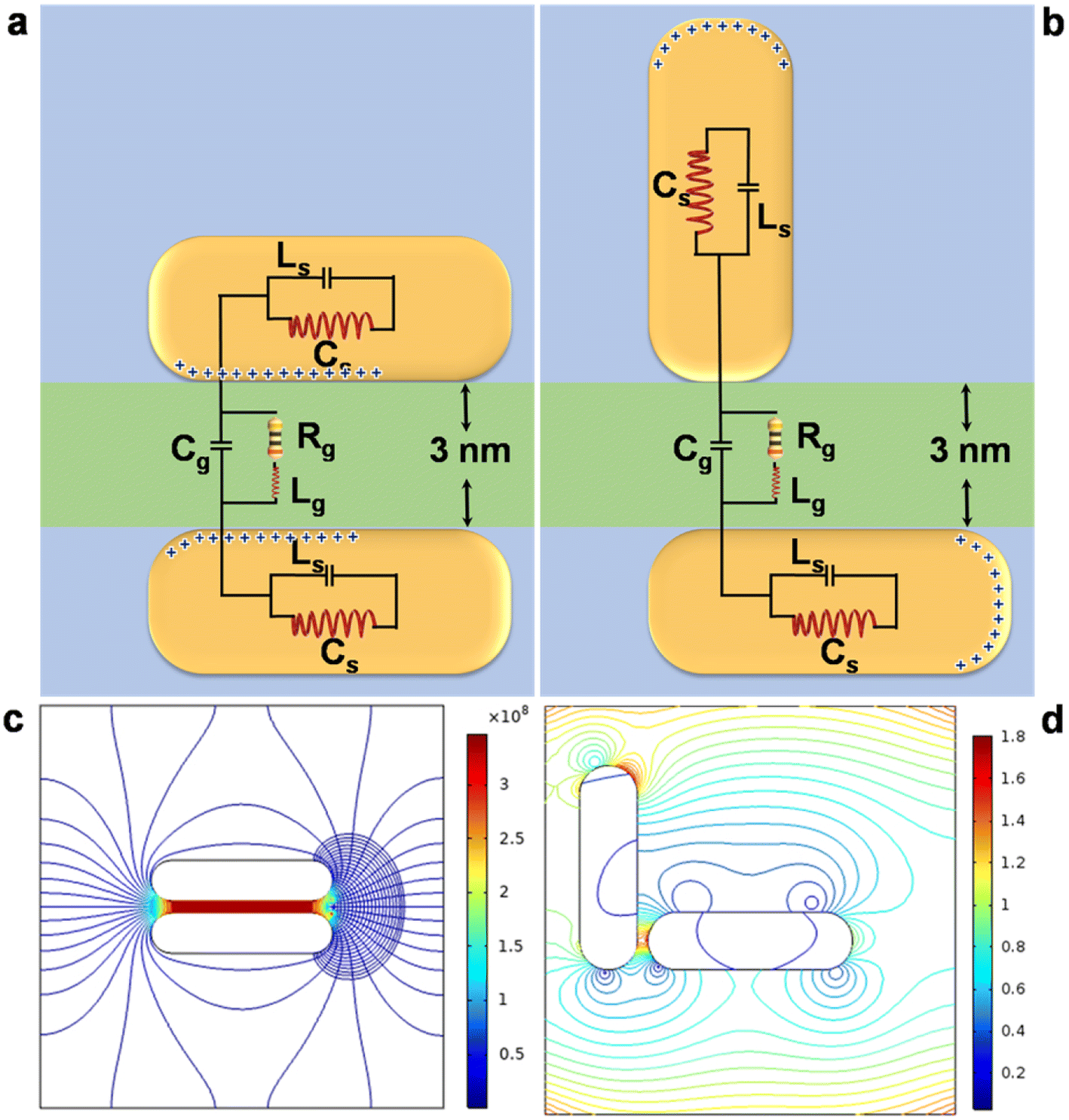
The dimers of the gold nanorods have been characterised by spectral and morphological studies as exhibited in Fig. 1. Panel a shows the ensemble-averaged absorption spectra of the monomers and upon aggregation of the nanorods. The monomeric gold nanorods exhibit transverse (∼557 nm) and longitudinal (∼732 nm) plasmon resonances corresponding to the divergence of electron oscillations along directions perpendicular and parallel to the length axis, respectively. However, upon the addition of organic ligands, the longitudinal resonance becomes blue and red shifted with maxima at ca. 714 and 741 nm, respectively, depending upon the orientation of the nanorods, while the transverse plasmon maximum remains nearly constant. The changes in the spectral positions can be attributed to the plasmon coupling between the gold nanorods; the relative decrease or increase in energy (relative to the longitudinal mode of a non-interacting rod) is indicative of the formation of gold nanorod dimers oriented in parallel and perpendicular directions, respectively. However, the polarisation of light along the direction perpendicular to the axis of the nanorods leads to excitation of the transverse mode and weak coupling between the nanorods does not impact the considerable shift of the plasmon resonance. The scattering spectra (panel b) measured at the single particle level closely resemble the absorption spectra corresponding to the monomeric and aggregated nanorods. The absorption and scattering spectra were found to be reproducible over a set of measurements. It is well documented that for the monomers, the peaks are relatively sharp, and the shift of longitudinal bands with the aspect ratio of the gold nanorods is quite distinctive. The discrimination between the monomers and dimers is due to the hybrid peaks in the longer wavelength region arising from the formation of plasmonic building units upon the addition of specific organic ligands; naked eye visualisation of the dimerisation process shows that the colour changes from reddish brown to dark or yellowish brown, indicating intrinsic morphological differences in the nature of the aggregates. Transmission electron micrographs (panels d–f) show monomeric gold nanorods with an average length of 55 ± 5 nm and width of 17 ± 2 nm (aspect ratio ∼ 3.2) and parallel and perpendicular dimers, respectively; the organic ligands bridge adjacent nanorods, manoeuvring them to be dimers. Dark field micrographs (panels g–i) display the corresponding polarisation modes of the individual nanorods and coupling between two degenerate plasmon modes of the nanorods in dimers.
 |
| | Fig. 1 Optical and structural characteristics (a) absorption and (b) scattering spectra of the monomeric and dimeric gold nanorods; (c) schematic depiction of the dimer formation from the monomeric building units upon addition of specific organic ligands; (d–f) transmission electron micrographs and (g–i) dark field microscopic images of the monomers and parallel and perpendicular dimers of gold nanorods. | |
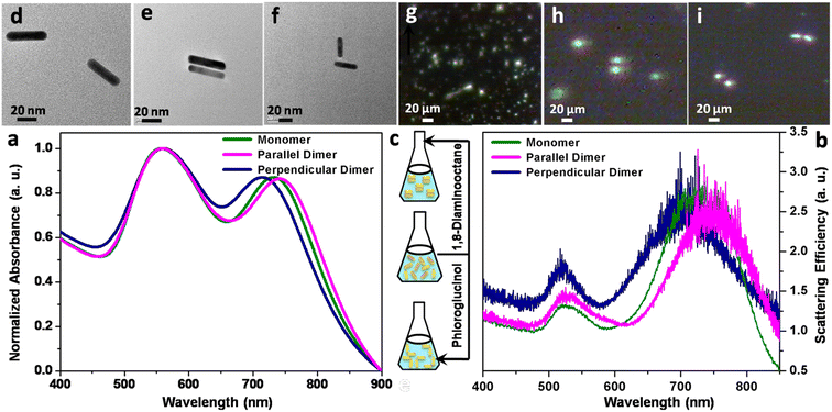
The electrodynamic interactions between gold nanorods as a function of the orientation angle were simulated based on DDA calculations, keeping the interrod distance fixed at ∼3 nm. The incident radiation is considered to be along the x-axis and the polarisation direction is along the y-axis. The extinction efficiency and the corresponding polarisation profiles for gold nanorod dimers at different mutual orientations are displayed in Fig. 2. It is noted that the extinction profile is highly dependent on the orientation angle between the optical axes of the nanorods (panel a). For these simulations, the position of one nanorod was assumed to be fixed and the other was varied with respect to the first. The relative rotation of the angle between the length axes of the coupled nanorods, θ, was considered around the z-axis (by varying θ in the DDSCAT code) on the xy-plane of the nanostructures and the excitation of the dimer was carried out at an incident angle, φ. The angle θ is considered to be the angle between the two nanorods in a dimer and φ is the angle of rotation of the working plane across the x-axis. A schematic illustration of the protocol for the angle-resolved measurements is shown in the inset. The continuous rotation of the second nanorod in the range of θ = 0° to 90° with periodic variation at an interval of 10° is observed. The distinct appearance of three peaks as indicated by the numbers 1, 2 and 3 can be attributed to the transverse, hybridised and longitudinal modes, respectively. The longitudinal mode develops due to orthogonal polarisation of the incident beam, which is not observed due to the collinearity of the beam with the axis of the parallel nanorods. The salient feature of physical significance is that the spectra show a decrease in intensity for transverse and longitudinal maxima, whereas the intensity of the hybridised peaks increases when the polarisation of the electric field is changed from the parallel to perpendicular orientations of the gold nanorod dimers. The hybrid peaks arise due to the near-field interaction between the coupled nanorods. The spectrum of the rod dimers at 0° follows the trend shown by the dimers at other angles but the third peak, which is caused by the longitudinal plasmon oscillation, becomes diminished in intensity. To realise the epicentre of the emergence of the different LSPR bands, the polarisations corresponding to the characteristic maxima of the transverse, hybridised and longitudinal peaks upon periodic variation of the orientation angle of 10° have been calculated (panels b–d). To obtain the polarisation profile, the wavelengths of the individual peaks at particular orientations have been calculated, and then the polarisations for the individual orientations have been determined corresponding to the three individual peaks of the gold nanorod dimers. It has been revealed that the gold nanorod dimers display strong polarisation dependence upon variation of the orientation angle between the nanorods. Thus, the polarisation profiles fundamentally represent the nature of the polarisation at the extinction peaks. At the 0° orientation, the double dumbbell-shaped polarisation profile can be attributed to the quadrupolar polarisation, while at 90°, the dumbbell shaped polarisation profile corresponds to a dipolar mode. As the angle between the nanorods increases from 0° to 90°, the quadrupolar mode gradually disappears with the concomitant appearance of the dipolar mode, as has been observed for gold nanorod dimers in two photon photoluminescence experiments.31 Calculations have shown that after crossing the limit of 90°, the scattering characteristics repeat, as the boundary conditions are in the range of 0–90° for the azimuthal angle, and, therefore, to explore all plausible sets of repeating patterns, we limit the calculations to this range.
 |
| | Fig. 2 Extinction and polarisation profiles (a) extinction spectra of gold nanorods dimers at different angular orientations calculated based on DDA technique; and (b–d) corresponding polarisation profiles at the wavelength maxima of the extinction profiles. The colour coded numerals 1, 2, 3 in panel a designate characteristic peaks for transverse, hybridised and longitudinal peaks at different angles of orientations. | |
The electric field distribution patterns at all the plausible geometries have been calculated by solving Maxwell's equations through the finite element method using an interval of the orientation angle of 10° assuming a constant interrod distance (∼3 nm), as presented in Fig. 3. To unravel the unprecedented dependence of the plasmonic properties of the dimers on the nanorod angle, the calculations were first performed for the longitudinal plasmon mode of the nanorod monomer to extract the requisite dimensional and dielectric parameters, because this plasmon mode was readily observed experimentally. The observation of an intense modification of the local electric field in the spatial regions of different geometries (panel a) indicates that the near-field interaction between the nanorods is highly angle-dependent.15,16,60 In addition, it is noted that the field intensity is at a maximum at the ‘hot spot’ junction between the coupled rods.15,16 As the orientation angle increases, the intensity at one end progressively decreases while the intensity reaches a maximum at the other end of the coupled dimer. It has been determined that the gold nanorods exhibit the appearance of both transverse and longitudinal modes with plasmon resonances arising from the polarisations orthogonal and along the length axis of the nanostructures. When two nanorods come into close proximity to one other, the plasmon resonances of the nanostructures lead to an electromagnetic interaction that can be treated within the framework of the plasmon hybridisation model,61 in analogy with molecular orbital theory, which predicts that upon dimerisation, the excited energy levels are split into lower and higher energy levels relative to the monomer. A plasmon hybridisation diagram has been produced to denote the energies corresponding to symmetric and antisymmetric arrangements of the transition dipoles (panel b). For parallel coupling, the higher coupled plasmon mode is bonding in nature while for perpendicular coupling, it exhibits antibonding character. The in-plane plasmon modes of the nanorod dimers were considered by assuming that the excitation light is polarised within the substrate plane either along or perpendicular to the nanorod angle. Based on this perspective, according to the plasmon hybridisation model,61 four hybridised plasmon modes are developed because each nanorod monomer possesses transverse and longitudinal plasmon modes. When the nanorod angle in the dimer is 0 and 90°, corresponding to the parallel and perpendicular orientations, respectively, the transverse and longitudinal modes are hybridised separately to exhibit the bonding and antibonding modes. The Schatz and Mirkin group62 have found that there exist many similarities between the nature of antibonding coupled modes in dimers/trimers and higher order plasmon resonances of the distinct nanorods of identical length. However, under the excitation of light polarised along the length axis of the nanorods, the parallel coupling of gold nanorod dimers has been experimentally found to exhibit a slightly red-shifted coupled plasmon mode, while perpendicular dimers support a largely blue-shifted coupled plasmon mode, as has been observed in the absorption and scattering spectral characteristics. The observation of a cross-over region at ca. 45° of the nanorod orientation (panel c) shows the existence of bonding and antibonding interactions with equal electric field intensities. This indicates that at the 45° orientation, the gap between the bonding and antibonding modes decreases to zero and the two states can be considered to be degenerate.
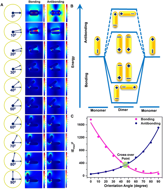 |
| | Fig. 3 Electric field distribution patterns of the bonding and antibonding modes (A) comparison of the electric field distribution patterns of the bonding and antibonding modes of the coupled gold nanorods at different orientation angles; (B) plasmon hybridization model of the coupled longitudinal plasmon excitation in nanorod dimers; and (C) profiles showing the variation in |E2| as a function of the orientation angle for the bonding and antibonding modes of the gold nanorod dimers. | |
Next, we tried to explore the dependence of the orientation angle on the electric field distribution patterns through the finite element method. The field distribution patterns corresponding to the transverse, hybridised and longitudinal maxima of the extinction profiles and the respective polarisation patterns obtained through DDA calculations are displayed in Fig. 4. It has been revealed that the electric field distribution patterns (panels A–C) are strongly dependent on the relative orientations of the coupled gold nanorods. The polarisation patterns (panel D) correspond to the transverse, hybridised and longitudinal maxima of the gold nanorod dimers at different angles of orientation. The intermediate peak arises due to plasmon hybridisation between the nanorods. Both polarisation profiles, at the intermediate and longitudinal maxima, at 0°, exhibit quadrupolar nature. As the angle between the nanorods increases, the polarisation profile changes, which can be ascribed to the disturbance of the symmetry of the organisation of the nanorods. The extent of change is greater in the case of the longitudinal than the intermediate or hybridised polarisation. This is due to the fact that as the angular displacement increases, the radial distance between the far ends of the rods is more than that between the near ends.
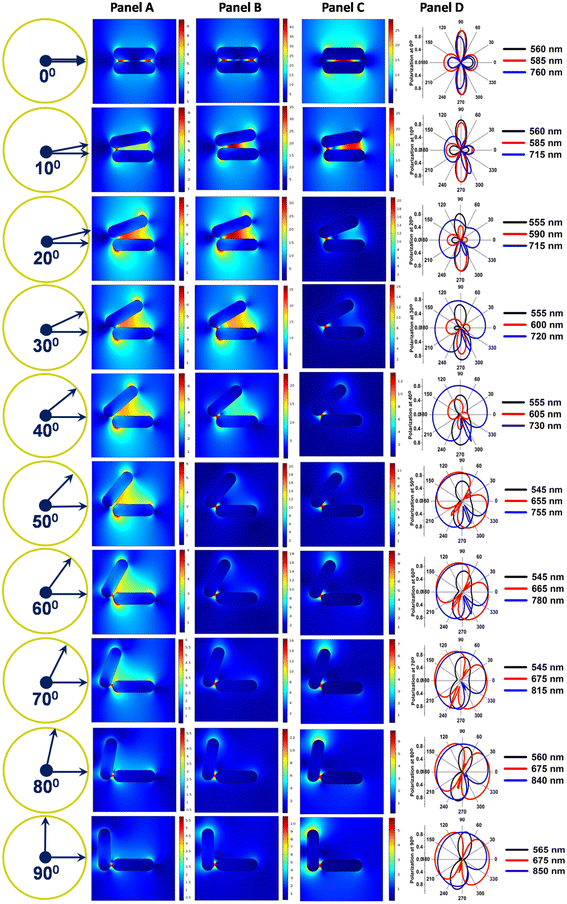 |
| | Fig. 4 Electric field distribution patterns corresponding to polarisation maxima (panels A–C) electric field distribution patterns corresponding to transverse, hybridised and longitudinal maxima; and (panel D) corresponding polarisation patterns for the respective wavelength maxima of the coupled nanorods in the extinction profiles obtained from DDA calculations. | |
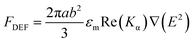
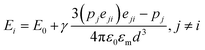
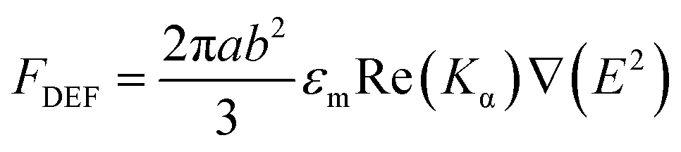
The rod-like nanostructures can be considered as prolate ellipsoidal particles with semi-major (a) and semi-minor (b) axes and the plasmonic characteristics can be treated within the framework of Gans' model at the limit of the quasistatic approximation. However, the dimerisation between two adjacent nanorods can be depicted as due to the electrostatic interaction between the two point dipoles centred at the nanorods. The time-averaged dielectrophoretic force, FDEF, experienced by a prolate ellipsoidal particle through the α-axis (where α = L,T designates longitudinal and transverse directions, respectively) oriented parallel to the direction of the electric field can be expressed as:63
| |  | (1) |
where
εm is the dielectric constant of the dispersion medium of the nanorods,
Kα the Clausius–Mossotti factor and
E the induced electric field. For a homogeneous nanorod, the electric polarisabilities (
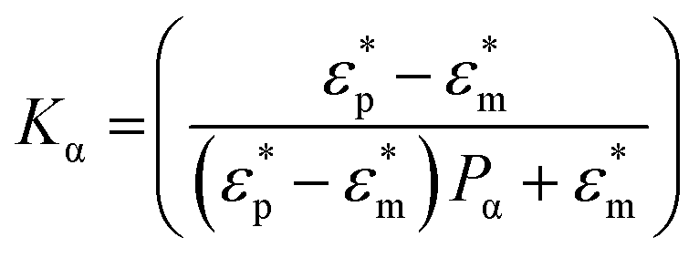
Kα) corresponding to the longitudinal and transverse plasmon modes based on the balance between the dielectrophoretic force and viscous torques can be written according to the Clausius–Mossotti equation as:
64| | 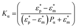 | (2) |
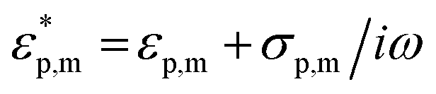
where the corrected dielectric functions are expressed as complex quantities,
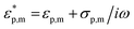
in which
εp,m and
σp,m represent the dielectric constants and conductivities of the particle and the dispersion medium, respectively,
ω the frequency of the applied electric field and
Pα the depolarisation factor of the nanorods. The depolarisation factors pertaining to the longitudinal and transverse plasmon modes of a prolate ellipsoid,
PL and
PT, respectively, can be described by the relations:
| | 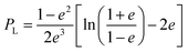 | (3) |
and
| |  | (4) |
where
e is the eccentricity

of the nanorods. From the transmission electron micrographs, the monomeric nanorod with
a = 55 and
b = 17 nm possesses the values of
e = 0.94,
PL = 0.11 and
PT = 0.95. When an external electric field is applied, the electric dipole moment,
pi of an individual
ith nanorod can be represented as:
64where
E0 is the incident electric field and
βi the electric polarisabilities (where
i =
B,
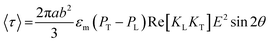
A assigns values corresponding to the bonding and antibonding plasmon modes, respectively). Therefore, when two nanorods are coupled to form a dimer, the total induced electric field on the nanorod
i,
Ei can be described as the sum of the incident electric field,
E0 and the field induced through the electric dipole of the second nanorod,
j as:
| |  | (6) |
where
d is the center-to-center distance between the two nanorods,
pj the electric dipole moment of the second nanorod,
eji the unit vector emanating from the center of the nanorod
j to the center of the nanorod
i and
γ a coefficient that can account for additional factors, such as the finite-size effect, multipolar contribution, charge redistribution and the substrate effect whenever applicable. As a consequence of the angular displacement between the nanorods, an optical torque (〈
τ〉) is generated at each orientation that can be calculated by the model proposed by the Poelsema group.
65 It has been observed that the optical torque between the nanorod dimers is dependent on the aspect ratio and the orientation angle as proposed by the equation:
| |  | (7) |
where
θ is the angular distortion between the coupled nanorods.
Fig. 5 shows the trend of the variation of the optical torque and the square of localised field strength as a function of the angular orientation. From the nature of the profiles, it can be seen that the functional behaviour is quite non-linear and asymmetric in the regime of the orientation angle under consideration. Surprisingly, it is observed that the optical torque is at a maximum at
ca. 22.5° orientation (panel a). On the other hand, the squared field strength reaches a maximum at the parallel configuration, while at the perpendicular orientation it reaches a minimum (panel b). It is noted that at an angular orientation of
ca. 45°, the longitudinal and transverse electric fields show a unique cross-over point due to the equivalent orientation of the dipole polarisation vectors. The apparent dichotomy in their functional behaviour is reflected through the non-linear nature of the surface plot, where the crest points become twisted in the
xy-plane (panel c). These results show that the maximum torque has been obtained for a distortion at an angular orientation of
ca. 22.5° of the swinging nanorod around the length axis of the basal nanorod.
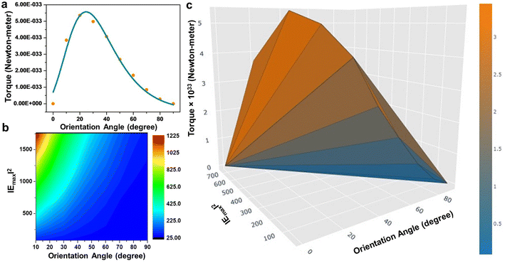 |
| | Fig. 5 Optomechanical characteristics (a) optical torque; and (b) electric field strength as a function of orientation angle of the gold nanorods; and (c) corresponding surface plot with the crest points twisted in xy-plane. | |
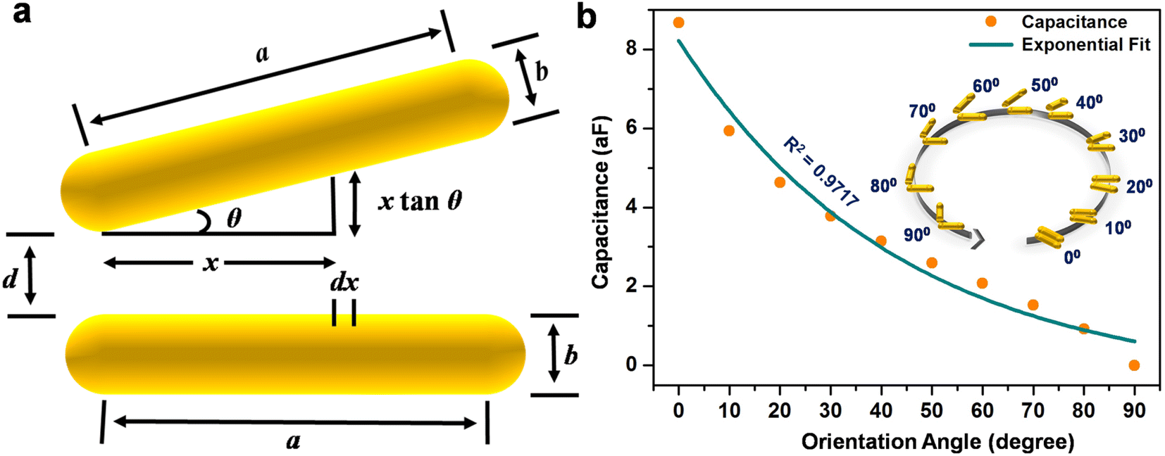
From the previous studies, it becomes evident that the optical properties of gold nanorods can be significantly altered upon dimerisation governed by optical torque66 and hence, it can be presumed that the mutual orientation of the gold nanorods in dimeric geometries can be utilised to store electrical energy in the form of capacitors. A capacitor can be considered as a device that stores electrical energy in the form of electric charge between two conductive parallel plates under the influence of an applied electric field. Therefore, capacitors are often referred to as electrical condensers to hold a voltage or potential difference in charge at equilibrium. Moreover, the high electrical conductivity and excellent faradaic effect of metallic gold warrants its application in electrical double layer capacitors. Therefore, the optomechanic characteristics of gold nanorod dimers can be investigated to exploit their plausible application in capacitors. The calculation of the capacitance of the gold nanorod dimers as a function of the orientation angle (keeping the position of one nanorod fixed, and with the dielectric constant of the medium assumed to be that of air) has been presented in Fig. 6. To model the capacitance, it can be assumed that the metallic gold at the nanoscale behaves as a perfect conductor so that the finite conductivity and skin-depth effect can be neglected.67 Panel a displays a schematic illustration of the arbitrary formation of a capacitor composed of a pair of nanorods. Let us consider a metallic nanorod with hemispherical end caps with a slit of length a, width b, closest end-to-end distance between two nanorods d, and displacement from the fixed end of the rotating nanorod x. The angular dependence of classical (geometric) capacitance (CC) upon variation of an angular parameter, θ can be calculated by the equation:
| | 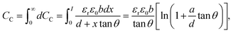 | (8) |
which can be simplified into the form:
| |  | (9) |
where
εr is the dielectric constant of metallic gold and
A the cross-sectional area of each nanorod. Details of the calculation are shown in the ESI.
† Between two electric point dipoles, at the semi-classical limit, where the nanocapacitor is composed of thousands of atoms, the quantum mechanical component,
CQ that arises because of the manifestation of the density of states of the metallic nanorods should also be taken into consideration.
68,69 Büttiker and co-workers
70 formulated a mathematical description for the quantum capacitance (
CQ) at very low frequencies:
| |  | (10) |
 |
| | Fig. 6 Angle-resolved design of the capacitor (a) schematic illustration of the arbitrary formation of a capacitor with angular orientation of nanorod dimers; and (b) the exponential decay fit of the calculated values of the capacitance at different angular orientations of the gold nanorod dimers. The inset in panel b shows a schematic presentation of the gold nanorod dimer at different mutual orientations. | |
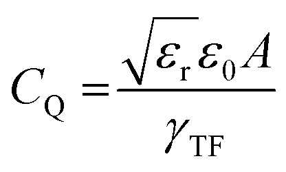
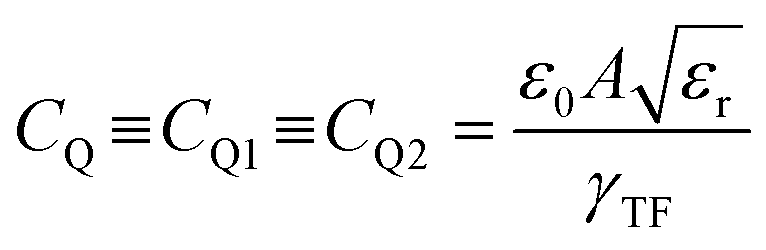
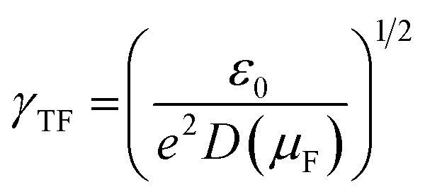
The Thomas–Fermi screening length term, γTF accounts for the penetration of the metallic nanorod surface by the incident electric field. The total capacitance (C) of the nanocapacitor due to the combination of both classical and quantum capacitance can be estimated as:
| |  | (11) |
When the metallic nanorods are composed of same material and geometrically identical, the density of states at the Fermi level of either nanorod, D(µF) = dn/dµ1 = dn/dµ2, where µ1 and µ2 are the electrochemical potentials, and under such conditions:
| |  | (12) |
where
,
e being the elementary charge of an electron
. Therefore, when two metal plates are of the same size and sufficiently large enough, the total capacitance can be simplified to the form:
| |  | (13) |
Incorporating the values of both classical and quantum capacitances, the total capacitance can be reduced to the form:
| |  | (14) |
The calculated values of the capacitance show an exponential decrease (panel b) upon angular variation from the parallel to perpendicular orientation, obeying the exponential dependence as predicted by the universal plasmonic ruler equation.60,71 Interestingly, the capacitance is at a maximum for the parallel and a minimum for the perpendicular orientations, while the fractional values of the capacitance are a measure of the degree of coupling between the nanorods. From the finite element method calculations, it has been seen that the electric field strength decreases as the angle between the nanorods increases. Therefore, it can be conceived that the increase in the angle causes the electric flux within the capacitor to decrease, as a result of which the capacitance decreases.
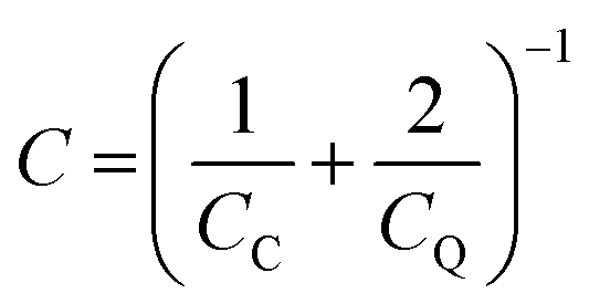
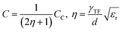
To verify the computational prediction, experiments have been performed with dimeric structures composed of discrete gold nanorods characterised by a net current as illustrated in Fig. 7. We have used an equivalent circuit shunted with a resistor and an inductor, which mimics the behaviour of conductive paths through the gap in series.72,73 Simplified pictures (panel a) show two conducting nanorods of equal dimensions connected to the power supply and the dielectric acts as the separator between the nanorods. Cs is the capacitance in series, Cg that of the dielectric, Rg the gate resistance, Ls the low power Schottky p–n junctions and Lg the gap inductance. Since there can be significant fringing fields around the capacitor plates (two nanorods), the size of the air volume truncates the modelling space. The electric fields at two different orientation angles (panel b) are relatively uniform between the plates, but strong variation is seen at the edges of the plates. The fringing fields are observed to extend a small distance away from the capacitor; a slice plot of the electric potential shows that there is an equipotential surface exactly midway between the capacitor plates.74 The capacitances of the devices are evaluated to be approximately 69 and 0 attofarads, respectively. The coupled bonding gold nanorod dimer (perpendicular) plasmon mode becomes blue shifted due to the screening of the local field in the gap. In this conductivity region, the screening field reduces the voltage between the two elements. The experimental observation is in good agreement with the computational predictions; however, the observed difference between the calculated and measured values can be attributed to the higher conductivities through a charge transfer mode in the parallel configuration. Thus, nanostructure dimerisation mimics parallel plate capacitance in conventional electrostatics and, therefore, can be considered for use in the basic elements in optical nanocircuits.
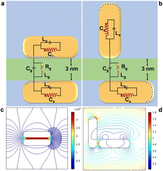 |
| | Fig. 7 Capacitive coupling (a, b) schematic diagram showing the capacitive coupling between the adjacent gold nanorods in dimers corresponding to parallel and perpendicular configurations, respectively; and (c, d) schematic depiction of the electric lines of force in dielectric medium surrounding the capacitor corresponding to parallel and perpendicular configurations, respectively. | |
4. Conclusions
In conclusion, we have determined the correspondence between plasmonics and electronics through the mechanics of gold nanorod dimers from both theoretical and experimental perspectives. It has been observed that for a particular interparticle distance, the orientation angle plays a deterministic role in governing the electrodynamic interactions between these anisotropic nanostructures. Spectral measurements and DDA calculations show that when metal nanorods are placed adjacent to each other, their localised surface plasmons are coupled together in accordance with the predictions of the plasmon hybridisation model and the appearance of a hybridised peak indicating the coupling of the adjacent nanorods at the hotspot junction. Finite element modelling shows that the field distribution changes with the orientational angle between the nanorods, the electromagnetic field being perpendicular to the plane of rotation. The confinement of the electric field in a small space can be exploited in surface enhanced spectroscopies that offer great potential for the use of light at the nanoscale. The concept of a homodimer can be extended to gold nanorod dimers with asymmetric monomeric lengths, varying interparticle distances and all plausible mutual orientations towards the generalisation of these observables. The fine tuning of the capacitance as a measure of the degree of coupling between the nanorods follows an exponential dependence similar to the universal plasmon ruler equation. The maximisation of the capacitance at an orientation of the gold nanorod dimers of 0° mimics the parallel plate capacitor model of conventional electrostatics. The main significance of these materials is that the interplay between the plasmonic characteristics and electrical capacitance of the coupled gold nanorods can lead to the formation of miniaturised nanocapacitors and, therefore, have the potential to form the basis for the design of all-optical neuromodulators, switches, integrated photonic circuits and microelectronic devices.
Conflicts of interest
There are no conflicts to declare.
Acknowledgements
We gratefully acknowledge financial support from DST-SERB, New Delhi (Project No.: EMR/2016/006842). We are thankful to Professor Nikhil R. Jana, IACS, Kolkata for providing facilities for zeta potential measurements.
References
- J. Li, Z.-H. Zhou, S. Wan, Y.-L. Zhang, Z. Shen, M. Li, C.-L. Zou, G.-C. Guo and C.-H. Dong, Phys. Rev. Lett., 2022, 129, 063605 CrossRef CAS PubMed.
- Z. Gan, J. Yin, X. Xu, Y. Cheng and T. Yu, ACS Nano, 2022, 16, 5131–5152 CrossRef CAS PubMed.
- F. Wen, Y. Zhang, S. Gottheim, N. S. King, Y. Zhang, P. Nordlander and N. J. Halas, ACS Nano, 2015, 9, 6428–6435 CrossRef CAS PubMed.
- V. G. Kravets, A. V. Kabashin, W. L. Barnes and A. N. Grigorenko, Chem. Rev., 2018, 118, 5912–5951 CrossRef CAS PubMed.
- M. E. Mann, P. Yadav and S. Kim, ACS Appl. Nano Mater., 2021, 4, 9976–9984 CrossRef CAS.
- Y. Kim, S. Cha, J.-H. Kim, J.-W. Oh and J.-M. Nam, Nanoscale, 2021, 13, 9541–9552 RSC.
- J. Zheng, X. Cheng, H. Zhang, X. Bai, R. Ai, L. Shao and J. Wang, Chem. Rev., 2021, 121, 13342–13453 CrossRef CAS PubMed.
- L. Scarabelli, A. Sánchez-Iglesias, J. Pérez-Juste and L. M. Liz-Marzán, J. Phys. Chem. Lett., 2015, 6, 4270–4279 CrossRef CAS PubMed.
- P. Pramod and K. George Thomas, Adv. Mater., 2008, 20, 4300–4305 CrossRef CAS.
- C. Ciracì, R. T. Hill, J. J. Mock, Y. Urzhumov, A. I. Fernández-Domínguez, S. A. Maier, J. B. Pendry, A. Chilkoti and D. R. Smith, Science, 2012, 337, 1072–1074 CrossRef PubMed.
- S. K. Ghosh and T. Pal, Chem. Rev., 2007, 107, 4797–4862 CrossRef CAS PubMed.
- N. J. Halas, S. Lal, W.-S. Chang, S. Link and P. Nordlander, Chem. Rev., 2011, 111, 3913–3961 CrossRef CAS PubMed.
- P. Nordlander, C. Oubre, E. Prodan and K. Li, Nano Lett., 2004, 4, 899–903 CrossRef CAS.
- J. Fontana and B. R. Ratna, Appl. Phys. Lett., 2014, 105, 011107 CrossRef.
- C. Tabor, D. van Haute and M. A. El-Sayed, ACS Nano, 2009, 3, 3670–3678 CrossRef CAS PubMed.
- L. Shao, K. C. Woo, H. Chen, Z. Jin, J. Wang and H. Q. Lin, ACS Nano, 2010, 4, 3053–3062 CrossRef CAS PubMed.
- J. Kumar and K. George Thomas, J. Phys. Chem. Lett., 2011, 2, 610–615 CrossRef CAS.
- P. Johns, R. J. Suess, N. Charipar and J. Fontana, J. Phys. Chem. C, 2019, 123, 15209–15216 CrossRef CAS.
- J. H. Yoon, F. Selbach, L. Schumacher, J. Jose and S. Schlücker, ACS Photonics, 2019, 6, 642–648 CrossRef CAS.
- C. Li, S. Li, A. Qu, H. Kuang, L. Xu and C. Xu, Adv. Funct. Mater., 2020, 30, 2001451 CrossRef CAS.
- D. Sivun, C. Vidal, B. Munkhbat, N. Arnold, T. A. Klar and C. Hrelescu, Nano Lett., 2016, 16, 7203–7209 CrossRef CAS PubMed.
- R. Deska, P. Obstarczyk, K. Matczyszyn and J. Olesiak-Bańska, J. Phys. Chem. Lett., 2021, 12, 5208–5213 CrossRef CAS PubMed.
- K. W. Smith, H. Zhao, H. Zhang, A. Sánchez-Iglesias, M. Grzelczak, Y. Wang, W.-S. Chang, P. Nordlander, L. M. Liz-Marzán and S. Link, ACS Nano, 2016, 10, 6180–6188 CrossRef CAS PubMed.
- D. E. Gömez, A. Roberts, T. J. Davis and K. C. Vernon, Phys. Rev. B: Condens. Matter Mater. Phys., 2012, 86, 035411 CrossRef.
- Z.-J. Yang, Z.-H. Hao, H.-Q. Lin and Q.-Q. Wang, Nanoscale, 2014, 6, 4985–4997 RSC.
- B. Auguié, J. L. Alonso-Gömez, A. Guerrero-Martínez and L. M. Liz-Marzán, J. Phys. Chem. Lett., 2011, 2, 846–851 CrossRef PubMed.
- Z. Chen, X. Lan, Y.-C. Chiu, X. Lu, W. Ni, H. Gao and Q. Wang, ACS Photonics, 2015, 23, 392–397 CrossRef.
- L.-Y. Wang, K. W. Smith, S. Dominguez-Medina, N. Moody, J. M. Olson, H. Zhang, W.-S. Chang, N. A. Kotov and S. Link, ACS Photonics, 2015, 2, 1602–1610 CrossRef CAS.
- L. A. McCarthy, K. W. Smith, X. Lan, S. A. H. Jebeli, L. Bursi, A. Alabastri, W.-S. Chang, P. Nordlander and S. Link, Proc. Natl. Acad. Sci. U. S. A., 2020, 117, 16143–16148 CrossRef CAS PubMed.
- J. Comenge, O. Fragueiro, J. Sharkey, A. Taylor, M. Held, N. C. Burton, B. K. Park, B. Wilm, P. Murray, M. Brust and R. Lévy, ACS Nano, 2016, 10, 7106–7116 CrossRef CAS PubMed.
- M. Garai, N. Gao and Q.-H. Xu, J. Phys. Chem. C, 2018, 122, 23102–23110 CrossRef CAS.
- A. Lee, A. Ahmed, D. P. dos Santos, N. Coombs, J. I. Park, R. Gordon, A. G. Brolo and G. Kumacheva, J. Phys. Chem. C, 2012, 116, 5538–5545 CrossRef CAS.
- S. Biswas, J. Duan, D. Nepal, K. Park, R. Pachter and R. A. Vaia, Nano Lett., 2013, 13, 6287–6291 CrossRef CAS PubMed.
- J. Kumar, X. Wei, S. Barrow, A. M. Funston, K. George Thomas and P. Mulvaney, Phys. Chem. Chem. Phys., 2013, 15, 4258–4264 RSC.
- X. Ben and H. S. Park, J. Phys. Chem. C, 2012, 116, 18944–18951 CrossRef CAS.
- S. Haq, T. E. Tesema, B. Patra, E. Gomez and T. G. Habteyes, ACS Photonics, 2020, 7, 622–629 CrossRef CAS.
- V. G. Aswathy, P. P. Patra and G. V. Pavan Kumar, J. Opt., 2015, 17, 114011 CrossRef.
- P. Pachidis, B. M. Cote and V. E. Ferry, ACS Appl. Nano Mater., 2019, 2, 5681–5687 CrossRef CAS.
- J. Kern, S. Großmann, N. V. Tarakina, T. Häckel, M. Emmerling, M. Kamp, J.-S. Huang, P. Biagioni, J. C. Prangsma and B. Hecht, Nano Lett., 2012, 12, 5504–5509 CrossRef CAS PubMed.
- G. Lu, L. Hou, T. Zhang, W. Li, J. Liu, P. Perriat and Q. Gong, J. Phys. Chem. C, 2011, 115, 22877–22885 CrossRef CAS.
- T. Kawawaki, H. Zhang, H. Nishi, P. Mulvaney and T. Tatsuma, J. Phys. Chem. Lett., 2017, 8, 3637–3641 CrossRef CAS PubMed.
- L. Wang, Y. Zhu, L. Xu, W. Chen, H. Kuang, L. Liu, A. Agarwal, C. Xu and N. A. Kotov, Angew. Chem., Int. Ed., 2010, 49, 5472–5475 CrossRef CAS PubMed.
- T. Zhang, N. Gao, S. Li, M. J. Lang and Q.-H. Xu, J. Phys. Chem. Lett., 2015, 6, 2043–2049 CrossRef CAS PubMed.
- L. Zhong, X. Zhou, S. Bao, Y. Shi, Y. Wang, S. Hong, Y. Huang, X. Wang, Z. Xie and Q. Zhang, J. Mater. Chem., 2011, 21, 14448–14455 RSC.
- K. D. Osberg, M. Rycenga, N. Harris, A. L. Schmucker, M. R. Langille, G. C. Schatz and C. A. Mirkin, Nano Lett., 2012, 12, 3828–3832 CrossRef CAS PubMed.
- I. Haidar, G. Lévi, L. Mouton, J. Aubard, J. Grand, S. L. Truong, D. R. Neuville, N. Félidj and L. Boubekeur-Lecaque, Phys. Chem. Chem. Phys., 2016, 18, 32272–32280 RSC.
- Y. Salamin, P. Ma, B. Baeuerle, A. Emboras, Y. Fedoryshyn, W. Heni, B. Cheng, A. Josten and J. Leuthold, ACS Photonics, 2018, 5, 3291–3297 CrossRef CAS.
- Z. Wang, R. Liu, H.-Y. Chen and H. Wang, JACS Au, 2021, 1, 1700–1707 CrossRef CAS PubMed.
- U. Bhattacharjee, C. A. West, S. A. H. Jebeli, H. J. Goldwyn, X.-T. Kong, Z. Hu, E. K. Beutler, W.-S. Chang, K. A. Willets, S. Link and D. J. Masiello, ACS Nano, 2019, 13, 9655–9663 CrossRef CAS PubMed.
- R. Melikov, S. B. Srivastava, O. Karatum, I. B. Dogru-Yuksel, H. B. Jalali, S. Sadeghi, U. M. Dikbas, B. Ulgut, I. H. Kavakli, A. E. Cetin and S. Nizamoglu, ACS Appl. Mater. Interfaces, 2020, 12, 35940–35949 CrossRef CAS PubMed.
- L. Xu, Y. Gao, H. Kuang, L. M. Liz-Marzán and C. Xu, Angew. Chem., Int. Ed., 2018, 57, 10544–10548 CrossRef CAS PubMed.
- M. Losurdo, F. Moreno, C. Cobet, M. Modreanu and W. Pernice, J. Appl. Phys., 2021, 129, 220401 CrossRef CAS.
- C. L. Kane, Phys. Rev. Lett., 2022, 128, 076801 CrossRef CAS PubMed.
- K. Yee, IEEE Trans. Antennas Propag., 1966, 14, 302–307 Search PubMed.
- B. T. Draine and P. J. Flatau, J. Opt. Soc. Am. A, 1994, 11, 1491–1499 CrossRef.
- P. B. Johnson and R. W. Christy, Phys. Rev. B: Solid State, 1972, 6, 4370–4379 CrossRef CAS.
- N. R. Jana, L. Gearheart and C. J. Murphy, Adv. Mater., 2001, 13, 1389–1393 CrossRef CAS.
- N. R. Jana, L. Gearheart and C. J. Murphy, J. Phys. Chem. B, 2001, 105, 4065–4067 CrossRef CAS.
-
E. J. W. Verwey, J. Th and G. Overbeek, in Theory of the Stability of Lyophobic Colloids, Elsevier, Amsterdam, 2006 Search PubMed.
- A. M. Funston, C. Novo, T. J. Davis and P. Mulvaney, Nano Lett., 2009, 9, 1651–1658 CrossRef CAS PubMed.
- E. Prodan, C. Radloff, N. J. Halas and P. Nordlander, Science, 2003, 302, 419–422 CrossRef CAS PubMed.
- K. D. Osberg, N. Harris, T. Ozel, J. C. Ku, G. C. Schatz and C. A. Mirkin, Nano Lett., 2014, 14, 6949–6954 CrossRef CAS PubMed.
- C. Y. Yang, Y. Lin and U. Leia, Appl. Phys. Lett., 2007, 90, 153901 CrossRef.
- M. Gluodenis and C. A. Foss Jr, J. Phys. Chem. B, 2002, 106, 9484–9489 CrossRef CAS.
- W. Ahmed, E. S. Kooij, A. van Silfhout and B. Poelsema, Nano Lett., 2009, 9, 3786–3794 CrossRef CAS PubMed.
- J. H. Kang, D. S. Kim and Q.-H. Park, Phys. Rev. Lett., 2009, 102, 093906 CrossRef CAS PubMed.
- W. Liu and E. McLeod, J. Phys. Chem. C, 2019, 123, 13009–13014 CrossRef CAS.
- K. J. Savage, M. M. Hawkeye, R. Esteban, A. G. Borisov, J. Aizpurua and J. J. Baumberg, Nature, 2012, 491, 574–577 CrossRef CAS PubMed.
- J. A. Scholl, A. García-Etxarri, A. L. Koh and J. A. Dionne, Nano Lett., 2013, 13, 564–569 CrossRef CAS PubMed.
- M. Büttiker, A. Prêtre and H. Thomas, Phys. Rev. Lett., 1993, 70, 4114–4117 CrossRef PubMed.
- K. C. Woo, L. Shao, H. Chen, Y. Liang, J. Wang and H.-Q. Lin, ACS Nano, 2011, 5, 5976–5986 CrossRef CAS PubMed.
- O. Pérez-González, N. Zabala, A. G. Borisov, N. J. Halas, P. Nordlander and J. Aizpurua, Nano Lett., 2010, 10, 3090–3095 CrossRef PubMed.
- F. Benz, C. Tserkezis, L. O. Herrmann, B. de Nijs, A. Sanders, D. O. Sigle, L. Pukenas, S. D. Evans, J. Aizpurua and J. J. Baumberg, Nano Lett., 2015, 15, 669–674 CrossRef CAS PubMed.
- J. Gabellig, G. Fève, B. Berroir, B. Placais, A. Cavanna, B. Etienne, Y. Jin and D. C. Glattli, Science, 2006, 313, 499–502 CrossRef PubMed.
Footnote |
| † Electronic supplementary information (ESI) available: Derivation of the capacitance of angle-resolved nanorod dimers. See DOI: https://doi.org/10.1039/d3na00061c |
|
| This journal is © The Royal Society of Chemistry 2023 |
Click here to see how this site uses Cookies. View our privacy policy here. 
 Open Access Article
 This Open Access Article is licensed under a Creative Commons Attribution-Non Commercial 3.0 Unported Licence
 *b
*b


 in which εp,m and σp,m represent the dielectric constants and conductivities of the particle and the dispersion medium, respectively, ω the frequency of the applied electric field and Pα the depolarisation factor of the nanorods. The depolarisation factors pertaining to the longitudinal and transverse plasmon modes of a prolate ellipsoid, PL and PT, respectively, can be described by the relations:
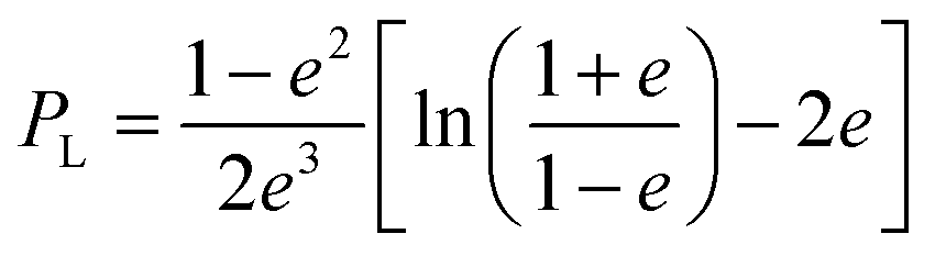

 of the nanorods. From the transmission electron micrographs, the monomeric nanorod with a = 55 and b = 17 nm possesses the values of e = 0.94, PL = 0.11 and PT = 0.95. When an external electric field is applied, the electric dipole moment, pi of an individual ith nanorod can be represented as:64


 , e being the elementary charge of an electron. Therefore, when two metal plates are of the same size and sufficiently large enough, the total capacitance can be simplified to the form: