
 Open Access Article
 This Open Access Article is licensed under a Creative Commons Attribution-Non Commercial 3.0 Unported Licence
A spectrally selective visible microbolometer based on planar subwavelength thin films†
Qianqian
Xu
ab,
Ziji
Zhou
ab,
Chong
Tan
ab,
Xiaohang
Pan
a,
Zhengji
Wen
 a,
Jinguo
Zhang
ac,
Dongjie
Zhou
ab,
Yan
Sun
a,
Xin
Chen
a,
Lei
Zhou
d,
Ning
Dai
ae,
Junhao
Chu
ac and
Jiaming
Hao
*ac
a,
Jinguo
Zhang
ac,
Dongjie
Zhou
ab,
Yan
Sun
a,
Xin
Chen
a,
Lei
Zhou
d,
Ning
Dai
ae,
Junhao
Chu
ac and
Jiaming
Hao
*ac
aState Key Laboratory of Infrared Physics, Shanghai Institute of Technical Physics, Chinese Academy of Sciences, Shanghai 200083, China
bUniversity of Chinese Academy of Sciences, Beijing 100049, China
cShanghai Frontiers Science Research Base of Intelligent Optoelectronics and Perception, Institute of Optoelectronics, Fudan University, Shanghai 200433, China. E-mail: jmhao@fudan.edu.cn
dState Key Laboratory of Surface Physics and Key Laboratory of Micro and Nano Photonic Structures (Ministry of Education), Physics Department, Fudan University, Shanghai 200433, China
eHangzhou Institute for Advanced Study, University of Chinese Academy of Sciences, Hangzhou 310024, China
First published on 23rd February 2023
Abstract
In this work, we experimentally demonstrate a new type of compact, low-cost, visible microbolometer based on metal–insulator–metal (MIM) planar subwavelength thin films, which exploits resonant absorption for spectral selectivity without additional filters and has the advantages of compact design, simple structure, cost-efficiency, and large format fabrication. The experimental results show that a proof-of-principle microbolometer exhibits spectrally selective properties in the visible frequency range. At a resonant absorption wavelength of 638 nm, a responsivity of about 10 mV W−1 is achieved at room temperature at a bias current of 0.2 mA, which is about one order of magnitude higher than that of the control device (a bare Au bolometer). Our proposed approach provides a viable solution for the development of compact and inexpensive detectors.
Introduction
Bolometers are a type of thermal detector in which the incident radiation is absorbed and converted to heat, resulting in temperature variation and thus the bolometer's electrical resistance change. This change can be detected by monitoring a bias current. Bolometric thermal detectors have been widely used in various applications1–4 ranging from thermal imaging and radiation temperature measurement to night vision and aerial navigation. In traditional bolometers, the incident radiation power is converted to heat by additional integrated absorbers that are bulky (compared to the operating wavelength) and generally have a flat broadband spectral response.5,6 However, a detector with spectrally selective characteristic is of significance in many application scenarios, such as color discrimination, biological sensing and chemical identification and analysis;7–11 more importantly, it is found that spectrally selective thermal detectors would have better performance than their broadband counterparts under certain specific conditions.11,12 There are a lot of methods for achieving spectral selectivity in thermal detection. Equipping with additional components,13–15 such as separate filters and interferometers, is a straightforward way, but this would increase the complexity and cost of the detection system. Plasmonic metamaterials composed of subwavelength artificially engineered meta-atoms have been explored to create bolometer detectors featuring resonant spectrally selective absorption over the past few years.16–20 For example, T. Maier and H. Brueckl implemented a square-shaped metal/dielectric/metal metamaterial absorber on conventional bolometer microbridges and demonstrated the possibility of tailoring the spectral response of the detectors in the mid-infrared spectral regime.21,22 F. B. P. Niesler, et al. proposed 4-shaped gold-nanostructure-based metamaterial bolometers, which take advantage of resonant absorption in that spectral selectivity can be obtained operating around optical communication wavelength.17 Chen et al. proposed an asymmetric subwavelength metamaterial microbolometer, which exhibits polarization insensitivity and frequency-selective high absorption over the long-wave infrared range.18 However, although spectral selectivity can be realized based on these strategies, the fabrication of such subwavelength artificial nanostructures is also elaborate and not cost-effective.In this paper, we propose and experimentally demonstrate a new type of compact, low-cost, visible microbolometer based on metal–insulator–metal (MIM) planar trilayer thin-film nanostructures, which is basically composed of a dielectric (Al2O3) layer sandwiched between two metal (Au) layers. The experimental results show that our proof-of-principle detector device exhibits a resonant absorption peak of around 0.76 at a wavelength of 638 nm. At the resonant absorption wavelength, a responsivity of about 10 mV W−1 is achieved at room temperature at a bias current of 0.2 mA, which is about one order of magnitude higher than that of the control device (a bare Au bolometer). Further characterization of the device reveals a thermal time constant of 2.14 ms and a noise equivalent power (NEP) of 131  . The proposed nanostructured devices present structural simplicity, scalable fabrication, and cost-efficiency characteristics and have a potential application prospect in color recognition.
Experimental section
Sample preparation
The fabrication of the proposed bolometer is straightforward and only utilizes one step of lithography processes, as schematically illustrated in Fig. 1(a)–(c). A clean quartz (SiO2) substrate with a size of 15 mm × 15 mm was first spin coated with a lift-off resist layer (LOR photoresist) and photoresist layer (AZ5214 photoresist). Then, laser direct writing lithography (MiScan, SVG Tech Group) was used to expose the photoresist to create a mask pattern. The next step is to deposit Au/Al2O3/Au tri-layer films at a rate of ∼2 Å s−1 by using electron beam evaporation. Finally, MIM thin film microbolometers with three different active areas 200 × 200 μm2 (denoted as MIM-200), 500 × 500 μm2 (MIM-500), and 800 × 800 μm2 (MIM-800), were obtained after the lift-off process (see Fig. S1, ESI†).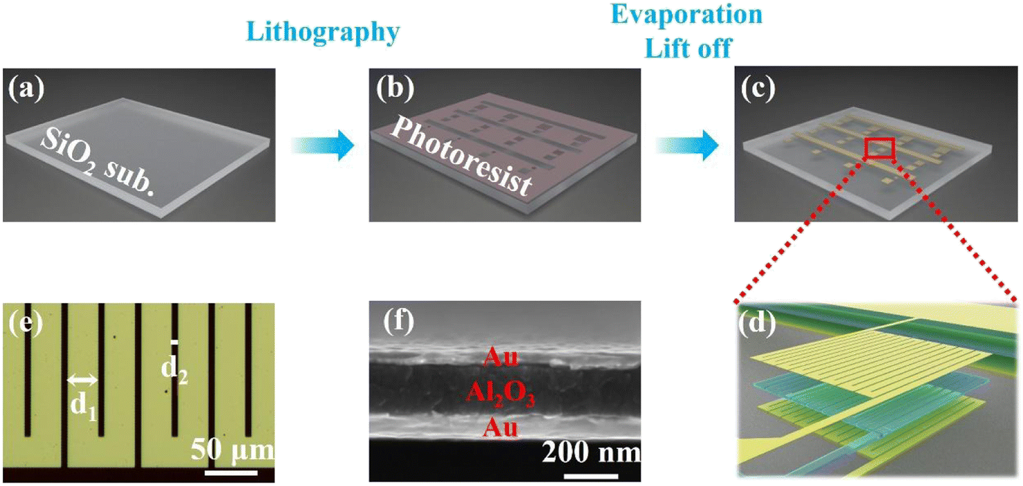 | ||
| Fig. 1 (a–c) Fabrication process of the proposed subwavelength thin-film-based microbolometers. (d) 3D schematic diagram of the proposed microbolometer. (e) Optical microscope image of the fabricated detector. (f) Cross-sectional SEM image of part of the fabricated sample. | ||
Characterization and measurements
An optical microscope (ECLIPSE Ci-S, Nikon) and a scanning electron microscope (SEM) (FEI Sirion 200) were used to characterize the morphologies of the fabricated bolometers. Reflection and transmission spectra of the fabricated devices were measured using a microscopic spectrometer (ARM, Ideaoptics). The measured reflectance spectrum is normalized with respect to a silver mirror. Therefore, the absorbance (A) can be calculated as A = 1 − R − T, where R and T represent reflectance and transmittance, respectively.Resistance measurement was carried out with a semiconductor analysis probe station equipped with a source meter (2636B Source-Meter, Keithley) and a temperature-controlled device (Model 336 Temperature Controller, Lakeshore). The simply calculated and measured resistance values for all fabricated devices are noted in Table S1, ESI,† The calculated resistance is obtained by using a simple formula R = ρ·l/s, where ρ, l, and s are the electrical resistivity, length, and cross-sectional area of the resistor, respectively. The discrepancies between the calculated and experimental resistances likely result from the heterogeneous electric current density in the winding shape, the simplification of calculations, and the experimental imperfections. Responsive measurement was implemented using an optoelectronic test system, including a light source (638 nm laser, Fiblaser; LEDs, Thorlabs), an optical chopper (SR540, Stanford Research Systems), a low-noise current preamplifier (SR570, Stanford Research Systems), and a lock-in amplifier (SR860, Stanford Research Systems). All of the spectral and electrical experiments were performed under normal atmospheric pressure and at room temperature.
Numerical simulations
The finite difference time domain (FDTD) method was employed to calculate the absorption properties of the MIM and bare Au structures. The complex dielectric constants of gold and alumina were obtained from the literature.23,24Results and discussion
We first performed computations to investigate the absorption of the MIM thin film nanostructure. The orange dashed line in Fig. 2(a) shows the calculated absorptance of the optimized planar MIM (34 nm Au, 130 nm Al2O3, and 100 nm Au) nanostructure as a function of wavelength. As a comparison, we also plot the absorption spectrum of the control sample (100 nm Au, denoted by planar bare Au) in Fig. 2(a) as a green dashed line. It is obvious that the planar MIM structure exhibits a nearly perfect absorption peak at a wavelength of 638 nm.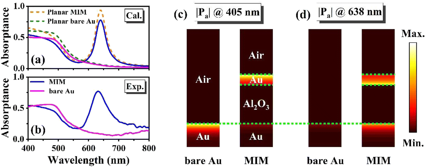 | ||
| Fig. 2 (a) Calculated absorption spectra of the MIM and bare Au structures. Here, the dashed lines correspond to the absorption spectra of planar structures and the solid lines correspond to the absorption spectra of winding structures. (b) Experimentally measured absorption spectra of the MIM and the bare Au microbolometers. The normalized time-averaged power dissipation density of both structures at 405 nm (c) and the resonance wavelength of 638 nm (d). | ||
In order to enhance the device's performance, we design a thermo-sensor as a winding shape to maximize the resistance of the device, as presented in Fig. 1(d) and (e). Fig. 1(e) shows an optical microscope image of part of the fabricated detector, where d1 and d2 denote the widths of the metal stripe and the gap, respectively. In our design, the duty ratio of the structure (d2/d1) is fixed as 1/5 for all the devices, namely d1 is set as 10, 25, and 35 μm for the devices MIM-200, MIM-500, and MIM-800, respectively, and d2 should be taken as 2, 5 and 7 μm in sequence correspondingly. The blue and pink solid lines in Fig. 2(a) show the calculated absorption spectra of the proposed winding-shape bolometer and its corresponding control sample. As expected, compared to the above planar MIM structure, the resonant absorption wavelength of the bolometer does not change, while the value of the absorption peak decreases and becomes around 80% due to the presence of the gaps. Fig. 2(b) presents typical experimental absorption spectra of the fabricated MIM bolometer and the control sample. As can be observed, at a wavelength of 638 nm, the absorption of the MIM bolometer is greatly enhanced and around 8 times larger than that of the bare Au control sample (see Fig. S2 for more detail, ESI†). Good agreements are found between the experimental and theoretical results.
To reveal the nature of such absorption enhancement effects, the time-averaged power dissipation density of the MIM device structure and the bare Au control samples is investigated. As shown in Fig. 2(c), at a wavelength of 405 nm, the absorption of the MIM structure is almost the same as that of the control samples; in both cases the incident light is absorbed near the surface of the conductor mainly related to interband absorption transitions.24 At a wavelength of 638 nm (Fig. 2(d)), the bare Au thin film has very weak absorption and strong reflection due to the impedance mismatch between the air and the gold film; while, the MIM device structure exhibits strong absorption, and both the top and bottom gold layers play important roles in the absorption effects, revealing that the remarkable enhancement of light absorption originated from the strong optical asymmetric Fabry–Perot resonant effect25 that significantly enhances the free electron contribution. Moreover, it should be noted that in all the cases the energy of incident light is dissipated by the metal and converted to heat eventually.
We now perform the thermal response measurements to reveal the performance of our bolometers. For bolometric detectors, the temperature coefficient of resistance (TCR) is a significant factor that manifests the sensitivity of a bolometric material to temperature changes, which is defined as α = dR/(R![[thin space (1/6-em)]](https://www.rsc.org/images/entities/char_2009.gif) dT),26 where R and T are the resistance and temperature, respectively. The TCR (α) of our bolometer is about 0.0014 K−1, which is obtained by measuring the resistance of the detector at different temperatures (see Fig. S3 in ESI†).17,18,27 The voltage responsivity (Rv) is given by Rv = ΔV/Φ0,where ΔV is the voltage change caused by Φ0, and Φ0 is the incident power.26Fig. 3(a) presents the adopted photo-thermal response testing system. The laser beam is first modulated using an optical chopper before illuminating the detector. The microbolometer subsequently converted the selectively absorbed light into an electrical signal, which was then amplified by the pre-amplifier, and finally collected using the lock-in amplifier. Fig. 3(b) shows the experimentally measured and numerically fitted responsivities for the device MIM-200 versus modulation frequency ranges from 5 to 1000 Hz. The experimental results of the MIM-500 and MIM-800 bolometers are presented in Fig. S4 (ESI†). Here, the laser power density is kept constant at 7.4 mW mm−2 and the bias current is set as 0.2 mA. As one can see, the maximum responsivity of the MIM-200 detector is about 10 mV W−1.
dT),26 where R and T are the resistance and temperature, respectively. The TCR (α) of our bolometer is about 0.0014 K−1, which is obtained by measuring the resistance of the detector at different temperatures (see Fig. S3 in ESI†).17,18,27 The voltage responsivity (Rv) is given by Rv = ΔV/Φ0,where ΔV is the voltage change caused by Φ0, and Φ0 is the incident power.26Fig. 3(a) presents the adopted photo-thermal response testing system. The laser beam is first modulated using an optical chopper before illuminating the detector. The microbolometer subsequently converted the selectively absorbed light into an electrical signal, which was then amplified by the pre-amplifier, and finally collected using the lock-in amplifier. Fig. 3(b) shows the experimentally measured and numerically fitted responsivities for the device MIM-200 versus modulation frequency ranges from 5 to 1000 Hz. The experimental results of the MIM-500 and MIM-800 bolometers are presented in Fig. S4 (ESI†). Here, the laser power density is kept constant at 7.4 mW mm−2 and the bias current is set as 0.2 mA. As one can see, the maximum responsivity of the MIM-200 detector is about 10 mV W−1.
 | ||
| Fig. 3 (a) Measurement setup for the bolometric response. (b) The responsivity of MIM and bare Au microbolometers as a function of modulation frequency, with the same efficient area size of 200 × 200 μm2. | ||
As for a thermal detector, the relationship between responsivity and modulation frequency can be described with the following equation:
 | (1) |
In order to experimentally characterize the spectrally selective properties of the fabricated microbolometer, additional responsive measurements of responsivity versus wavelength for MIM and bare Au microbolometers are conducted. The experimental setup is similar to that presented in Fig. 3(a), but changing the laser to LEDs with various wavelengths and adding a focusing lens (operating wavelength range of 200–2500 nm and a focal length of 60 mm) served to focus the incident light onto devices. During the test, the light power densities received by the detectors are controlled to around 1.2 mW mm−2 at all wavelengths. Fig. 4(a)–(f) display the experimentally measured and calculated spectral responsivities of two types of bolometers with different sizes and good agreements are noted between the experimental and calculated results. For the MIM devices, the maximum response peak wavelength at 638 nm is observed, while the bare Au devices exhibit very weak response for the wavelength range longer than 600 nm. The overall behavior of the experimental response is in accordance with the absorption spectra shown in Fig. 2(b). It is demonstrated that spectrally resolved detection can be achieved through our compact MIM microbolometer design. More notably, in contrast to the bare Au detectors, the utilization of the MIM structure in detectors effectually improves the performance in terms of responsivity and responsive time. The validity of our approach can thus be fully proved.
 | ||
| Fig. 4 Experimentally measured and calculated responsivity wavelength dependence of MIM and bare Au devices with an efficient area size of 200 × 200 μm2 (a and b), 500 × 500 μm2 (c and d) and 800 × 800 μm2 (e and f), respectively. (g and h) Experimentally measured and calculated absorption spectra. | ||
We further investigate the size dependence of the detector response. Fig. 5(a) shows the experimental peak responsivities for different detector sizes extracted from Fig. 4. Fig. 5(b) shows the corresponding η/G, the ratio of the absorption coefficient η to the effective thermal conductance G (see ESI† Note 1 for more details of the calculations for G and η/G). It is found that the responsivities are fitted to an exponential decay with the increment of the detector size, and the decay of η/G features similar behavior. This is consistent with the representation of the Rv, indicating that the performance of the microbolometer is strongly related to the absorption and the effective thermal conductance.
 | ||
| Fig. 5 Size-dependent exponential voltage responsivities (a) and the ratio of the absorption coefficient η to effective thermal conductance G (b). | ||
For a detector, its performance is not only determined from the responsivity, but it also depends on the noise of the detector. The dominant noise for metal bolometers is the Johnson noise, which originates from the Brownian motion of metal electrons.26 Therefore, the Johnson noises of the fabricated microbolometers can be calculated based on resistance, operating temperature (T) and electrical bandwidth (Δf) with the following equation:
 | (2) |
Subsequently, the noise equivalent power (NEP) of the detector can be obtained according to:
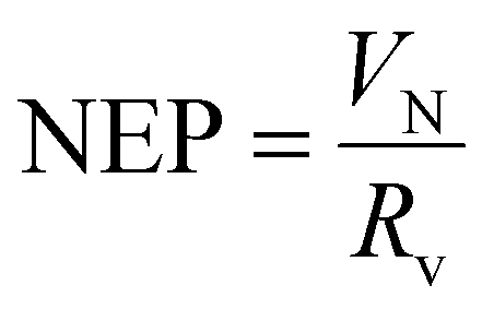 | (3) |
The Johnson noise is found to be 1.31 nV Hz−1 and 1.38 nV Hz−1 for the MIM microbolometer and bare Au microbolometer with the same efficient area size of 200 × 200 μm2, and the corresponding NEP at 5 Hz is 131 nW Hz−1 and 115 nW Hz−1, respectively. Finally, the specific detectivity of the fabricated detectors can be calculated using:
 | (4) |
Compared to commercial thermal detectors,26,28 the D* of our proposed microbolometer is relatively low. We infer that the reason for this is mainly due to two factors: (1). the lack of a thermal isolation bridge significantly increases the thermal conductance, and thus reduces the sensitivity and detectivity of the device.29 (2). The TCR of gold is lower than that of semiconducting oxides such as vanadium oxide,30 manganese cobalt nickel oxides31,32etc., hence limiting the properties of our microbolometers.
Conclusions
In summary, we have presented a new type of compact, low-cost, MIM planar trilayer thin-film structure-based bolometer operating at the visible band, without complicated preparation methods such as multi-phase photolithography and electron beam lithography. As a control, bare Au microbolometers are fabricated, which possess the same geometric parameters as MIM microbolometers but without the Al2O3 layer and the top Au layer. All of the microbolometers are fabricated with one step of direct laser writing lithography. The experimental results show that the fabricated devices exhibit spectrally selective properties, and good agreement between the absorption spectra and the measured responsivity spectra is observed. Furthermore, as a result of the strong field confinement of the MIM structure, the performance of the MIM microbolometer is significantly improved; around a 9-fold enhancement of responsivity at the resonant wavelength is obtained compared to that of the bare Au microbolometer. Size dependence of the performance of the detector has been experimentally investigated on our microbolometers. It is observed that the responsivity decreases and the time constant increases as the active area size increases; this mainly results from the thermal conductance and the thermal capacity of the detectors varying with the active area size, leading to a change in detectivity.Although our experiment only presents visible MIM microbolometers in this paper, one can modify the thickness of each thin film layer and alter materials to realize MIM microbolometers operating at any desired wavelength spanning from visible to infrared.25,33 Moreover, the performance of the microbolometer could be further improved by reducing the active area size and reforming the package of the detector, such as equipping it with a heat-insulating bridge to reduce the thermal conduction.29 We believe that our proposed planar thin film-based MIM microbolometer offers a viable way towards the development of miniaturized and inexpensive detectors.
Author contributions
Q. X. fabricated the samples, performed the measurements, analyzed the data, and wrote the original draft of the manuscript with assistance from Z. Z., C. T., X. P., Z. W., J. Z., and D. Z. Y. S. got the funding and supervised the fabrication of samples. X. C. supervised the measurements. L. Z., N. D., and J. C. were involved in the evaluation and interpretation of the results. J. H. conceived the research, got the funding, and wrote the manuscript. All the authors contributed to the discussion and revision of the manuscript.Conflicts of interest
The authors declare no conflicts of interest regarding this article.Acknowledgements
This work was supported by the National Key R&D Program of China (2022YFA1404701 and 2017YFA0205800), National Natural Science Foundation of China (62075231), Shanghai Science and Technology Committee (20JC1414603), Shanghai Innovation Project (2021-cyxt1-kj04) and China Postdoctoral Science Foundation (2021M703335).References
-
W. A. Radford, D. F. Murphy, A. Finch, A. Kennedy, J. K. Kojiro, M. Ray, R. Wyles, R. Coda, E. A. Moody and S. T. Baur, Infrared Detect. Focal Pl. Arrays V, 1998, vol. 3379, p. 22 Search PubMed
.
- Q. Zhang, R. Yan, X. Peng, Y. Wang and S. Feng, Mater. Res. Express, 2022, 9, 012002 CrossRef
- S. Sánchez, M. Elwenspoek, C. Gui, M. J. M. E. De Nivelle, R. De Vries, P. A. J. De Korte, M. P. Bruijn, J. J. Wijnbergen, W. Michalke, E. Steinbeiß, T. Heidenblut and B. Schwierzi, J. Microelectromech. Syst., 1998, 7, 62–67 CrossRef
- G. A. Wurden, B. J. Peterson and S. Sudo, Rev. Sci. Instrum., 1997, 68, 766–769 CrossRef CAS
- Y. H. Man, K. T. Kim, H. J. Shin, S. Moon and I. H. Choi, Appl. Phys. Lett., 2005, 86, 254101 CrossRef
- S. Sedky, P. Fiorini, K. Baert, L. Hermans and R. Mertens, IEEE Trans. Electron Devices, 1999, 46, 675–682 CrossRef CAS
-
S. J. Eames, J. S.-J. Yoo, J. C. Warner, D. P. Neikirk and J. T. McDevitt, in Engineered Nanostructural Films and Materials, SPIE, 1999, vol. 3790, pp. 160–168 Search PubMed
- C. Zhang, T. Xue, J. Zhang, L. Liu, J. Xie, G. Wang, J. Yao, W. Zhu and X. Ye, Nanophotonics, 2022, 11, 101–109 CrossRef CAS
- J. Shim, J. Lim, D.-M. Geum, B. H. Kim, S.-Y. Ahn and S. Kim, Opt. Express, 2021, 29, 18037 CrossRef CAS PubMed
- J. A. Montoya, Z.-B. Tian, S. Krishna and W. J. Padilla, Opt. Express, 2017, 25, 23343–23355 CrossRef CAS PubMed
- J. W. Stewart, N. C. Wilson and M. H. Mikkelsen, ACS Photonics, 2021, 8, 71–84 CrossRef CAS
- J. J. Talghader, A. S. Gawarikar and R. P. Shea, Light: Sci. Appl., 2012, 1, e24 CrossRef
- P. G. Lucey, K. A. Horton and T. Williams, Appl. Opt., 2008, 47, F107–F113 CrossRef PubMed
- D. Manolakis, S. Golowich and R. S. Dipietro, IEEE Signal Process. Mag., 2014, 31, 120–141 Search PubMed
- M. Meinig, S. Kurth, M. Seifert, K. Hiller, J. Wecker, M. Ebermann, N. Neumann and T. Gessner, Adv. Fabr. Technol. Micro/Nano Opt. Photonics IX, 2016, 97590W, 87 Search PubMed.
- S. Jiang, J. Li, J. Li, J. Lai and F. Yi, Opt. Express, 2022, 30, 9065 CrossRef CAS PubMed
- F. B. P. Niesler, J. K. Gansel, S. Fischbach and M. Wegener, Appl. Phys. Lett., 2012, 100, 203508 CrossRef
- C. Chen, Y. Huang, K. Wu, T. G. Bifano, S. W. Anderson, X. Zhao and X. Zhang, Opt. Express, 2020, 28, 28843 CrossRef CAS PubMed
- T. D. Dao, A. T. Doan, S. Ishii, T. Yokoyama, C. Niikura, S. Miyajima, T. Nabatame, T. Nagao, H. Sele Ørjan, D. H. Ngo, T. Ohki, A. Ohi, Y. Wada, C. Niikura, S. Miyajima, T. Nabatame and T. Nagao, Micromachines, 2019, 10, 416 CrossRef PubMed
- S. Jiang, J. Li, J. Li, G. Zhang, H. Liu and F. Yi, Opt. Express, 2020, 28, 22617 CrossRef CAS PubMed
- T. Maier and H. Brückl, Opt. Lett., 2009, 34, 3012–3014 CrossRef PubMed
- T. Maier and H. Brueckl, Opt. Lett., 2010, 35, 3766–3768 CrossRef CAS PubMed
-
E. D. Palik, Handbook of Optical Constants of Solids, Academic Press, 1985 Search PubMed
- P. B. Johnson and R. W. Christy, Phys. Rev. B: Solid State, 1972, 6, 4370–4379 CrossRef CAS
- Q. Xu, Z. Wen, X. Pan, C. Tan, J. Zhang, Q. Qiu, Y. Sun, X. Chen, N. Dai, J. Chu and J. Hao, Appl. Phys. Express, 2022, 15, 082005 CrossRef
-
A. Rogalski, Infrared Detectors, 2010 Search PubMed
- R. B. Belser and W. H. Hicklin, J. Appl. Phys., 1959, 30, 313–322 CrossRef CAS
- R. Ambrosio, M. Moreno, J. Mireles, A. Torres, A. Kosarev and A. Heredia, Phys. Status Solidi, 2010, 7, 1180–1183 CrossRef CAS
- C. F. Middleton and G. D. Boreman, J. Vac. Sci. Technol. B Microelectron. Nanom. Struct., 2006, 24, 2356 CrossRef CAS
- D. Lee, D. Kim, D. S. Kim, H. R. Park, C. Sohn, S. Namgung, K. Chung, Y. C. Jun, D. K. Kim, H. Choo and Y. G. Roh, Sci. Rep., 2021, 11, 15863 CrossRef CAS PubMed
- Y. Hou, Z. Huang, Y. Gao, Y. Ge, J. Wu and J. Chu, Appl. Phys. Lett., 2008, 92, 202115 CrossRef
- C. Ouyang, W. Zhou, J. Wu, Y. Hou, Y. Gao and Z. Huang, Appl. Phys. Lett., 2014, 105, 022105 CrossRef
- R. Yang, C. Dai, C. Wan, G. Zheng and Z. Li, Opt. Mater. Express, 2020, 10, 532 CrossRef CAS
Footnote |
| † Electronic supplementary information (ESI) available. See DOI: https://doi.org/10.1039/d2na00937d |
| This journal is © The Royal Society of Chemistry 2023 |