
 Open Access Article
 This Open Access Article is licensed under a Creative Commons Attribution-Non Commercial 3.0 Unported Licence
Mapping complex profiles of light intensity with interferometric lithography†
Joseph
Holmes
a,
Mi
Zhang
b,
Tine
Greibe
b,
William L.
Schaich
a,
Stephen C.
Jacobson
 *b and
Bogdan
Dragnea
*b
*b and
Bogdan
Dragnea
*b
aPhysics Department, Indiana University, Bloomington, IN 47405, USA
bDepartment of Chemistry, Indiana University, Bloomington, IN 47405, USA. E-mail: jacobson@iu.edu; dragnea@iu.edu; Tel: +1-812-8560087
First published on 6th March 2023
Abstract
Solving Maxwell's equations numerically to map electromagnetic fields in the vicinity of nanostructured metal surfaces can be a daunting task when studying non-periodic, extended patterns. However, for many nanophotonic applications such as sensing or photovoltaics it is often important to have an accurate description of the actual, experimental spatial field distributions near device surfaces. In this article, we show that the complex light intensity patterns formed by closely-spaced multiple apertures in a metal film can be faithfully mapped with sub-wavelength resolution, from near-field to far-field, in the form of a 3D solid replica of isointensity surfaces. The permittivity of the metal film plays a role in shaping of the isointensity surfaces, over the entire examined spatial range, which is captured by simulations and confirmed experimentally.
Introduction
The ability to map electromagnetic field distributions in the vicinity of nanostructures with sub-wavelength spatial resolution and over large lateral distances relative to the wavelength is important in the study of optical phenomena that stem from the interplay between evanescent and propagating fields such as in nanofocusing,1,2 Anderson localization in arrays of resonators with partial disorder,3 radiation forces in evanescent fields,4,5 and near-field thermovoltaic energy conversion.6 For any computational approach, capturing both field propagation and focusing sets serious computer processing power demands in terms of numbers of grid nodes and time steps. Moreover, the complex dielectric constant of metallic nanostructures can be affected by the fabrication process either via compositional purity or structural phase. Uncontrolled variations in these parameters are difficult to account for in simulation models. Nor, can they be all captured in the form of a convenient, lumped parameter to be included in a Maxwell solver. Therefore, having an experimental method that complements the computational approaches and is able to map complex field patterns over spatial scales running from tens of nanometers to several microns is beneficial.Here, we discuss an interferometric lithography approach, which builds on previous work for simpler systems.7–10 Aizenberg et al. first showed the possibility of mapping the electric field intensity distributions in the close vicinity of a grating phase mask by using a photoresist.7,8 In their work, all-dielectric media and a two-dimensional, periodic pattern allowed for a simplified theory. Amarie et al.9 adapted this scheme to allow mapping intensity profiles for a single nanoaperture in a thin metal film. The measured lithographic features compared favorably with isointensity surface predictions from a finite-difference time-domain (FDTD), three-dimensional Maxwell solver, which included dispersive effects in the metal film modeled by a Drude dielectric function.9 In terms of applications, a related approach used a two-dimensional array hyperbolic metamaterial to demonstrate large area deep sub-wavelength interference lithography.11 Plasmon polaritons played in this case a central role in obtaining sub-wavelength lithographic resolution.12
In this work, we extend the method to treat more complicated, lower symmetry patterns than previously examined. Complex patterns arise when multiple, subwavelength apertures are used in a metal film. The results indicate that good agreement can be obtained between lithographic replicas of the isointensity surfaces of light emerging from the apertures in different metals and FDTD simulations of the same, provided the specific metal's dielectric function is utilized in the simulations. In addition, as a potential application of the complex field patterns explored here, our simulations show that a specific polygonal hole pattern can generate sharp optical gradients above the structure, which could be useful for gradient-force optical trapping for on-chip sensing, particle sorting, and ion trapping applications.13
A typical example of the calculations featured in this work is shown in Fig. 1, which outlines the problem of finding the shape of isointensity surfaces from simulations. The basic geometry consists of a three layer system, which from bottom to top oriented along +ẑ, is a glass substrate, a metal film, and finally a polymeric negative tone photoresist. The origin for the z-axis is at the bottom surface of the metal. The finite nanoaperture array in Fig. 1A is a row of N = 3 cylindrical holes each of radius (r = d/2 = 50 nm) arranged with a center-to-center spacing set at a = 220 nm in a h = 100 nm thick metal film (Al in this case, Cr later). The photoresist fills each hole, in addition to the region z > h. Fig. 1B shows the calculated electric field intensity distribution (in fractions of the incident field intensity) for the geometry laid out in Fig. 1A when a plane wave of light with vacuum wavelength λ0 = 365 nm is incident from below and the metal is Al. The strong intensity within and just above the holes has intentionally been left white (and off the color scale) in order to allow a better visualization of the weak intensity emanating from the holes. This plotting scheme will also be used in later figures. The dotted lines denote boundaries of the metal film while along the pair of solid white curves the intensity is constant. In a full 3D view these curves become the isointensity surfaces which will be compared with a lithographic replica.
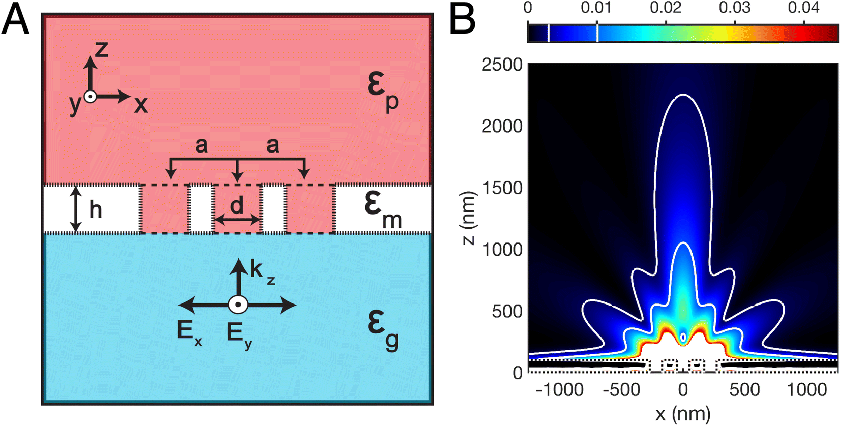 | ||
| Fig. 1 (A) Example of sub-wavelength hole array geometry to be studied and (B) corresponding FDTD simulation of intensity in fractions of the incident field intensity over the xOz plane. A plane wave impinges onto the Al film from below. The two white contour lines correspond to field intensity fractions of 0.003 (outer) and 0.01. | ||
Experimental structures are determined by exposure dose, Φ(![[r with combining right harpoon above (vector)]](https://www.rsc.org/images/entities/b_char_0072_20d1.gif) ), which is the product of the local electric field intensity, I(), and an exposure duration, τ. Corresponding intensity values are determined in computations from a double average of the square of the total electric field above the metal film.
), which is the product of the local electric field intensity, I(), and an exposure duration, τ. Corresponding intensity values are determined in computations from a double average of the square of the total electric field above the metal film.
I() = 〈〈|![[E with combining right harpoon above (vector)]](https://www.rsc.org/images/entities/i_char_0045_20d1.gif) tot(,t)|2〉〉 tot(,t)|2〉〉 | (1) |
The double, angled brackets denote averages over both a single period of the light and its incident polarization. A description of how averages are obtained from FDTD fields is given in the ESI (section “Averages”†). Assuming that exposure doses above a certain threshold, Φth, result in cross-linked polymer, the isointensity surface corresponding to this threshold will closely resemble the interface between the cross-linked polymer and non-crosslinked material. The latter can be subsequently removed (see below) leaving behind a three-dimensional replica of the isointensity surface corresponding to the threshold exposure. From the experiment one knows the exposure time and incident intensity. Because we are assuming that the Maxwell equations are linear in the fields, it follows that I() is linearly related to the incident intensity. This relation allows a comparison of theory and experiment without explicitly determining Φth: we calculate for each configuration of apertures the total electric field due to a specific, but arbitrary, incident electric field amplitude. Then we use graphic software (Matlab) to draw several isointensity surfaces. As the intensity value decreases with distance from the source, the corresponding isointensity surface grows in size and evolves in shape. By visual comparison with the measured surface profiles, we usually find a reasonable match, as will be shown later. When the exposure duration is the same for a series of aperture configurations, a simpler analysis scheme may be used (ESI, section “Isosurface intensity values”†).
Methods
Computational
Maxwell's equations were solved via the FDTD method within the total field/scattered field scheme,14 with commercially available software (Ansys/Lumerical 2022). The calculations were performed on a four-dimensional Yee grid, with a uniform lattice constant of Δxyz = 5 nm and time step Δt such that cΔt < Δxyz/√3 for stability.14 At the boundaries, perfectly matched layers completely enclose the simulation volume and truncate the simulation domain. A constant index of refraction is assigned to both the glass, ng = 1.47, and the polymer, np = 1.68,15 while for the metals (Al or Cr) a complex-valued, frequency-dependent relative permittivity was interpolated from a compilation of experimental results.16 The resulting permittivities for Al and Cr are shown in Fig. S1.† The boundaries between different media are sharp, and we do not consider spatial dispersion in the optical response. In our computations we assume that changes in the polymer index as it is exposed are negligible. This assumption preserves linearity in the computational model and is justified because direct post-exposure changes are minute, the polymer resist being chemically amplified.A transmission spectrum for a single hole in each metal (Al or Cr) film was obtained from the total fields by direct integration of the z-component of the Poynting vector across an observation plane slightly above the metal layer. Moreover, such transmission spectra were normalized by the incident flux striking a single hole and plotted versus the ratio d/λ0 where d is the hole diameter and λ0 is the vacuum wavelength of the light.
Experimental
Three-dimensional (3D) nanoscale structures were formed in a negative-tone photoresist by interference contact lithography9 and compared with isointensity surfaces obtained from the full 3D FDTD simulations. Cr or Al films were coated onto glass substrates (D263, Precision Glass & Optics) by either thermal evaporation (Edwards Auto 306) or by magnetron sputtering (purchased directly from Telic Co.). The nominal thickness of the metal films was 100 nm. We explored two different designs of nanoaperture arrays (aperture diameter: 100 nm) in each metal: (1) linearly coupled nanoapertures consisting of 1, 2, 3, and 4 apertures and (2) circular arrays of nanoapertures (with and without a central aperture) consisting of 4, 6, and 8 apertures on the perimeter. The center-to-center distance for the apertures in the linear arrays ranged from 150 nm to 2000 nm. The radius of the circular arrays measured from the array center to an outer aperture center was 275 nm.Note that, although the approach relies on a one-photon lithography process its spatial resolution is not determined by the diffraction limit. At very low doses, for instance, only subwavelength near-fields in the vicinity of the metal features will have sufficient intensity to exceed the polymerization dosage, as demonstrated in previous work.9
All nanoapertures were patterned with the Nano Pattern Visualization Engine (FIBICS Corp.) and milled into the metal film with a focused ion beam (FIB) instrument (Auriga 60, Carl Zeiss, Inc.). The ion beam used had an accelerating voltage of 30 kV and beam current of 5 pA, and the average dose was 0.8 nC μm−2 to generate apertures that passed through the metal film but minimally penetrated the glass substrate. The aperture diameters and spacing were measured with the scanning electron microscope (SEM) on the FIB instrument.
After FIB milling, the metal films were cleaned, spin coated with an adhesion promoter (2% titanium diisopropoxide bis(acetylacetonate) in isopropanol), and spin coated with a negative tone photoresist (AZ nLOF2070, 8 μm thick, n = 1.68 per product data sheet, from Integrated Micro Materials). The photoresist was soft baked (110 °C for 5 min) and subsequently exposed from the backside of the glass substrate with a collimated UV source at 365 nm (i-line, 10.2 mW cm−2, model 200, Optical Associates, Inc.). With constant irradiance, the exposure time was varied to produce total incident energy fluxes ranging from 1220 to 35![[thin space (1/6-em)]](https://www.rsc.org/images/entities/char_2009.gif) 000 mJ cm−2. Following a post-exposure bake (110 °C for 1 min), the photoresist was developed in MF-319 developer (Kayaku Advanced Materials, Inc.) to reveal the 3D nanostructures on the metal film. To characterize these structures, the substrates were sputter coated with 3 nm of gold/palladium prior to imaging with the SEM.
000 mJ cm−2. Following a post-exposure bake (110 °C for 1 min), the photoresist was developed in MF-319 developer (Kayaku Advanced Materials, Inc.) to reveal the 3D nanostructures on the metal film. To characterize these structures, the substrates were sputter coated with 3 nm of gold/palladium prior to imaging with the SEM.
We note that, throughout this study, we have employed a nominal wavelength of 365 nm fixed by the photoresist, but the methods are not limited to this wavelength or the UV wavelength range. For instance, commercial, chemically-amplified photoresists exist that work down to 436 nm (e.g., S 1813), without changes in the protocols described here. Moreover, Dika et al. have discussed the development of chemically-amplified lithographic resists for near-IR wavelengths17 while Fourkas reviewed alternate nanoscale photolithography approaches with visible wavelengths, most notably those using photochromic sensitizers.18
Results and discussion
Single aperture
Before we explore the radiation patterns due to finite arrays of coupled sub-wavelength apertures, we first turn our attention, as a control, to the interaction of light with a single, cylindrical hole in Al or Cr and compare their properties and transmission behavior to that of an identical hole in a perfect metal (PM) film to see how the differences in electric permittivities between a PM and a real metal affect the light transmission through a sub-wavelength hole in a metal film.Hans Bethe was the first to treat analytically the problem of light diffraction from a sub-wavelength hole. The expression he derived for the normalized transmittance,  , predicts a strong dependence on the dimensionless quantity d/λ0.19 This result for the transmittance was later extended to include higher order terms in d/λ0 by Bouwkamp.20 Still, the basic result in the Bethe–Bouwkamp analysis is that for an aperture in an idealized metal that is much smaller than the wavelength of the incident photon the transmittivity is very small.19,20
The strong starting assumptions of the Bethe model, including a PM screen of negligible thickness, cannot accurately predict the optical behavior of an aperture in a real metal film of finite thickness. This behavior was clearly illustrated by the discovery of extraordinary optical transmission through sub-wavelength hole arrays. For some metals and at certain wavelengths, substantially-enhanced transmission through a sub-wavelength aperture array in a metal film can occur.21 There is still (except for slits) a smooth cutoff in the limit of very long wavelengths, but its location and shape above the cutoff are sensitive functions of system details.
To illustrate the range of optical behaviors of a single sub-wavelength aperture, several transmission spectra of a cylindrical hole with (d = h = 100 nm) in a PM, Cr, and Al film are shown in Fig. 2A–C, respectively. For each metal, the dielectric environment is varied on either side of the aperture's entrance represented by different curves in Fig. 2A–C and labeled according to the relative permittivity on either side of the aperture as εz<0/εz>0.
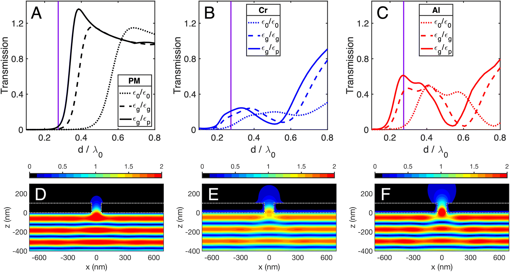 | ||
| Fig. 2 Transmission spectra for a single cylindrical hole in a PM (A), Cr (B), and Al (C) film. The vertical line is at λ0 = 365 nm. A transmission of unity corresponds to a number of photons transmitted being equal to the number of photons incident on the area of the hole. (D–F) Corresponding electric field intensity maps for cases (A–C) for λ0. | ||
The transmission spectra are quite different so we concentrate on the behaviors near the cutoffs and start with the simplest case of a PM film in Fig. 2A. If the film is suspended in vacuum, its cutoff is around d/λ0 = 0.5. When the metal is instead completely surrounded by glass there is a red shift of the cutoff location. When the dielectrics are arranged around the metal as in Fig. 1, there is a additional red shift of the cutoff region. We attribute these shifts mostly to changes in the local wavelength inside the hole. One has there λ = λ0/n with n changing from 1 to 1.47 to 1.68 for the three cases of Fig. 2A.
Turning to transmission spectra for Cr and Al in Fig. 2B and C, the same trends for red shifts of the cutoff regions are evident. However, for the vacuum wavelength used in this paper (λ0 = 365 nm), the transmission is much stronger in the metals than in the PM, with Al's transmission being stronger than Cr's. This increased transmission is further evidenced by the intensity profiles in Fig. 2D–F where a deeper field penetration into and through the hole can be seen. More detailed arguments for the enhanced field propagation through the real metal holes are given in the ESI† where we model the inside of a hole as a waveguide.
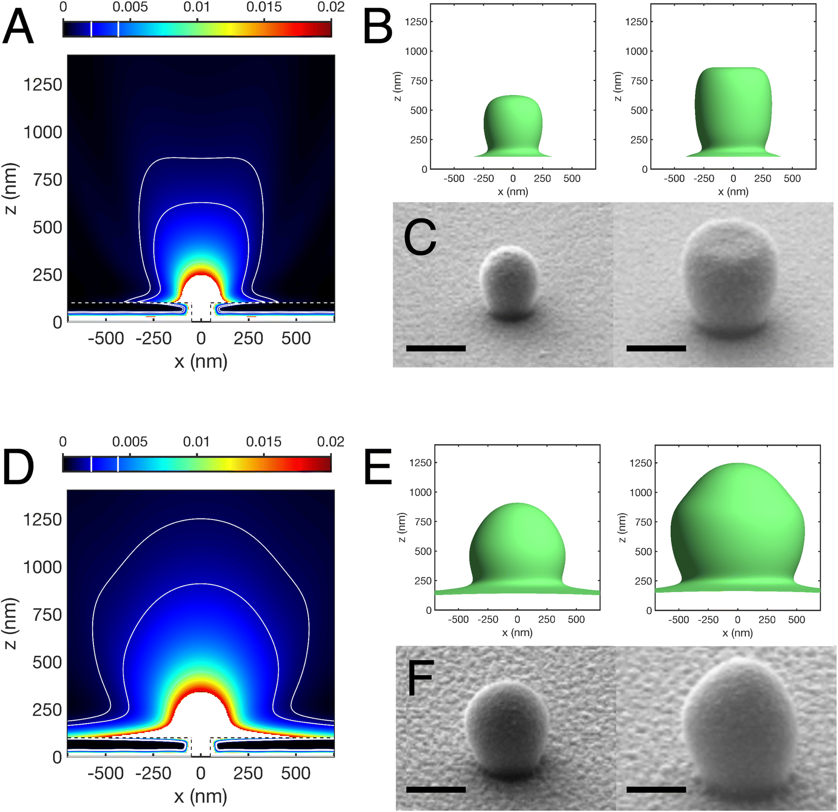
We now examine the ability of the lithographic approach to render details of the expected differences between Cr and Al films. Fig. 3A and D show in the xz-plane (at y = 0) the calculated intensity distribution (expressed as a fraction of the incident field intensity) emerging from a single cylindrical aperture along with a pair of isointensity curves for each metal. The corresponding 3D isointensity surfaces are displayed in Fig. 3B and E, respectively. The intensities for these surfaces have been chosen so their appearances best match the measured lithographic profiles in Fig. 3C and F. The measurements used a common incident irradiance, but the exposure time differed by a factor of two for the pair of replicas for each metal. For the simulations we note that: (i) although the calculations use the same incident irradiance for both metals, the predicted z-height for a fixed intensity is ∼75% higher for Al than for Cr, (ii) the top of the isointensity surface is flatter for Cr than for Al, and (iii) Al has a shoulder feature near its top and a “skirt” at its base which extends laterally more than the skirt around the Cr aperture.
 | ||
| Fig. 3
I() distribution for Cr (A) at 365 nm, two relevant isointensity surfaces (B), and a comparison with the lithographic structures (C) in Cr are given in the top panel. I() distribution for Al (D), two relevant isointensity surfaces (E), and a comparison with the lithographic structures (F) in Al are given in the bottom panel. Scale bar: 500 nm. Contour lines (white) correspond to field intensity fractions of 0.002 and 0.004. | ||
Qualitatively, the different shapes of the polymer replicas compare well with the numerical calculations. From SEM, the two different polymer structures imaged for each metal differed in size and shape dependent on the exposure dose applied during the experiment. The experimental incident energy flux used for the lower dose was 17.5 ± 0.1 J cm−2 (left SEM image in Fig. 3C and F) and this value doubled to 35.0 ± 0.1 J cm−2 for the higher dose (right SEM image in Fig. 3C and F). Consistent with our earlier discussion, the intensity levels for the best match between the pairs of simulations and replicas also differ by a factor of two. For Cr the replicas begin rounded, mostly egg-shaped, and develop at the higher exposure dose a flat top. In contrast for Al, a bulge near the top of the replica becomes more pronounced at the lower intensity level. It is worth noting here that being able to adjust the exposure at will gives substantial control of which isointensity surface is mapped. nLOF is a chemically amplified resist which means that it has an all-or-nothing response, with a cross-linking density vs. exposure being well approximated by a step function with a threshold at ≈100 mJ cm−2.22 The uptake ramp of this steep crosslink/exposure step-function determines the experimental uncertainty in the position of the isointensity surface or the spatial resolution of the approach. In any case, innermost isointensity surfaces are accessible by reducing exposure as exemplified in Fig. 3. Even hollow structures, such as those later described in this paper, should be in principle accessible through the use of focused ion beam cross-sectioning.
Multiple apertures
Here, we explore the application of the lithographic mapping technique to study the interference patterns from finite collections of cylindrical apertures arranged in 1D or 2D patterns in Cr or Al films. In all cases d = h = 100 nm and the incident electric field amplitude was kept the same. We begin with rows of holes with center-to-center spacing set to a = 300 nm to match the dimensions of the structures used in the lithographic mapping experiment. The strong similarity between calculated and experimental maps is apparent in Fig. 4. The agreement supports the assumptions made at the onset of calculations, in particular: (i) sharp metal film boundaries and (ii) existence of a threshold of exposure dose for transforming the resist. Notable are high intensity bands above the surface emerging within one wavelength from the surface from in between adjacent apertures. They are especially intense in the case of Al and their intensity increases with the number of holes in the array, Fig. 4A1–F1. Isointensity surfaces obtained for 1D multiple holes in Al are significantly larger in extent along the surface than in Cr. An intriguing difference between the two metals occurs for four holes in Fig. 4C2, C3, F2 and F3 where a peak along the z-axis is either absent or present, respectively. Note that for all the threshold intensity isosurfaces in the second row of Fig. 4 (as well as in Fig. 5 and 6) we used the same value of intensity fraction. This approach is reasonable because the experiments used the same incident irradiance and exposure time (see ESI section “Isointensity surface values”† for details).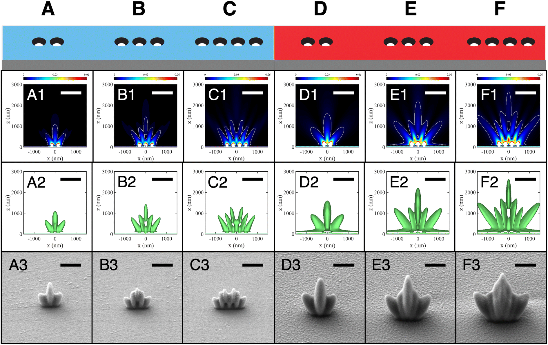 | ||
| Fig. 4 1D periodic arrangement of metallic nanoapertures for Cr (A–C) and Al (D–F). Row 2 shows the calculated intensity distributions for each case, and the solid white line indicates the value of the contour used in corresponding plots of the isointensity surfaces shown in row three. The corresponding polymer replicas obtained in the experiments are given in row four. Contour lines all correspond to a field intensity fraction of 0.007. Scale bar: 1 μm and the color scales for A1–F1 are linear and identical. | ||
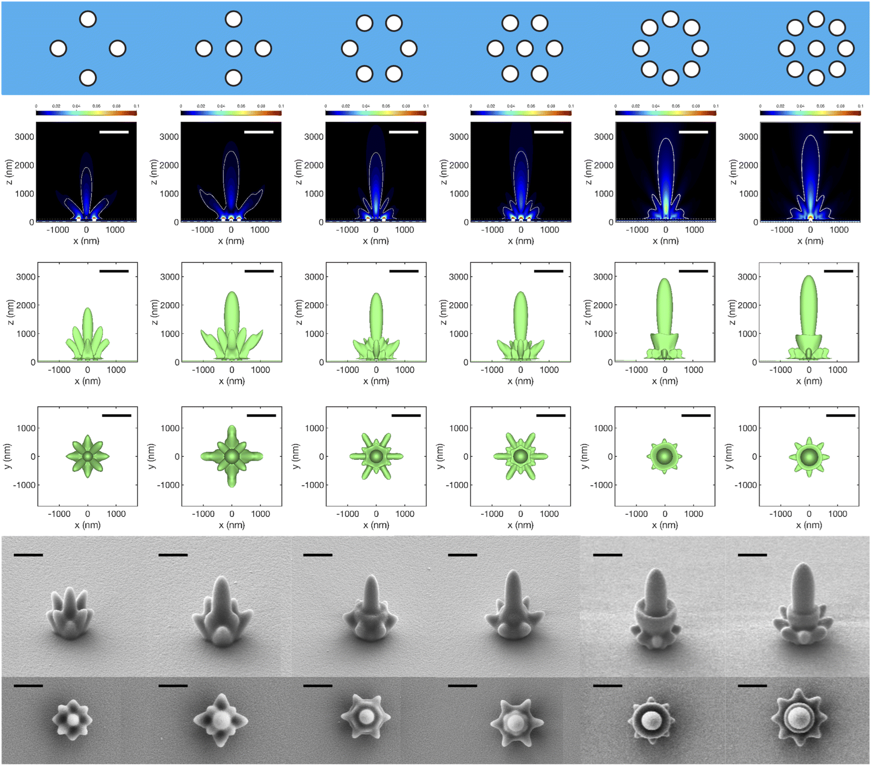 | ||
| Fig. 5 Top: Row 1: Schematic of 2D arrangements of metallic apertures in Cr, with or without a central aperture. Rows 2–4: Calculated fractional intensity profiles and isointensity surfaces. The white contours in row 2 correspond to a field intensity fraction of 0.007. The color scales for the intensity plots are linear and identical. Rows 5 and 6: Scanning electron micrographs for the corresponding lithographic replicas. Scale bar: 1 μm. | ||
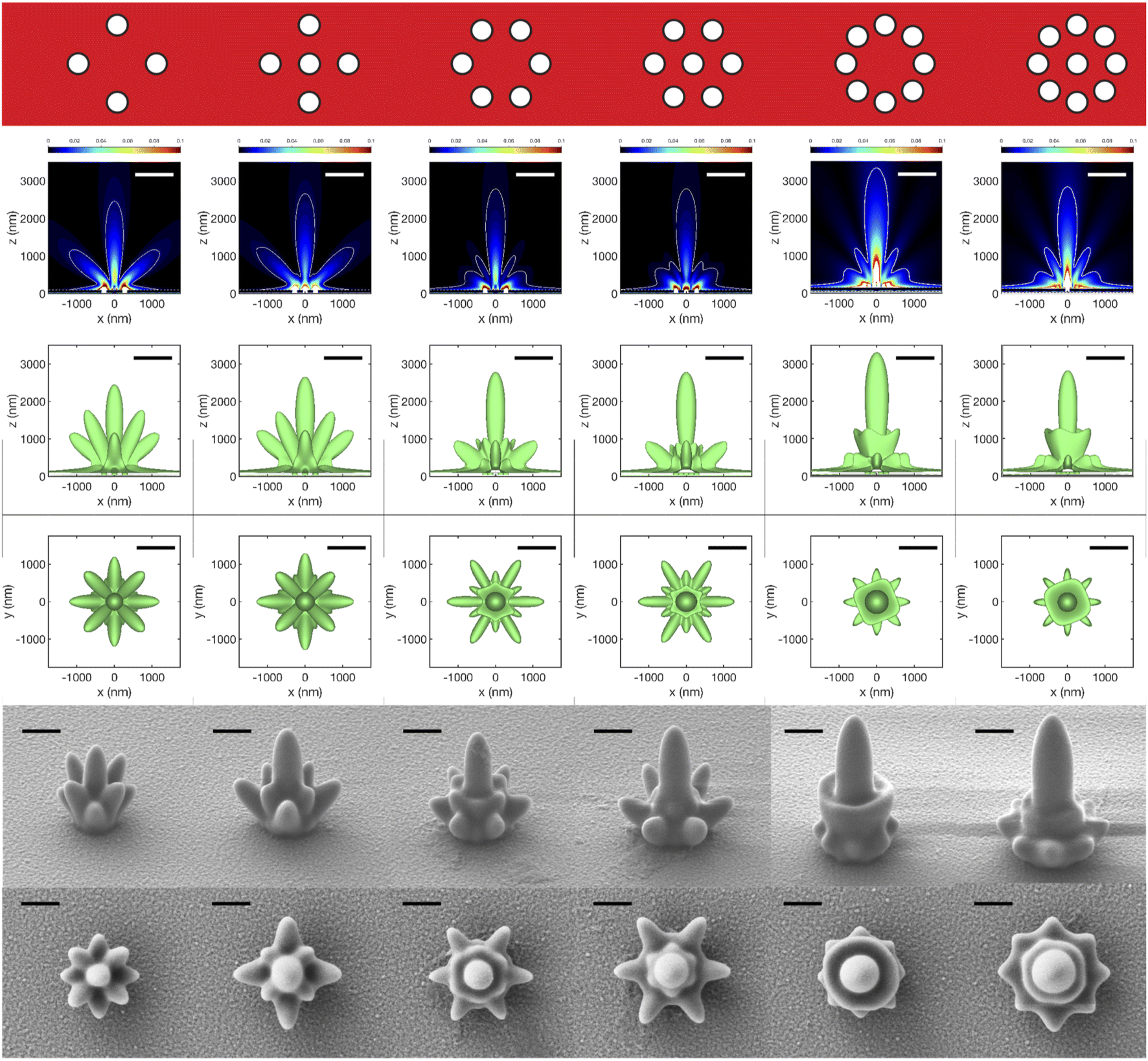 | ||
| Fig. 6 Row 1: Schematic of 2D arrangements of metallic apertures in Al, with or without a central aperture. Rows 2–4: Calculated fractional intensity profiles and isointensity surfaces. The white contours in row 2 correspond to a field intensity fraction of 0.007. The color scales for the intensity plots are linear and identical. Rows 5 and 6: Scanning electron micrographs for the corresponding lithographic replicas. Scale bar: 1 μm. | ||
The overall agreement between simulations and the proximity lithographic mapping approach presented so far for different patterns, metals and exposure doses opens the question of the inverse problem, i.e., whether determining the complex permittivity of the metal film from knowledge of the field and metal film topographic maps is possible. In the light of the results presented here, this intriguing possibility suggests a promising open direction for future research.
Turning to 2D arrays, the metallic nanostructures in Fig. 5 (Cr) and 6 (Al) have apertures arranged around a central point, thus forming finite collections with a discrete rotational symmetry. The motivation for these arrangements was to attempt to concentrate light intensity above the metal surface and centered on x = y = 0. Indeed, a central cigar-shaped structure develops in all these patterns, and its reach above the surface extends with more apertures in the set. There is an intriguing difference with the 8 member rings – between having a central hole or not. The latter is predicted by the FDTD simulations to produce more intense fields and a higher central isosurface feature. However, in the experimental replicas for these arrangements, the central isosurface feature is instead slightly higher when a central hole is present. The cause of this discrepancy is unclear at the moment but one may speculate that the surface modes are damped by film roughness and interfere less with the homogeneous (propagating) waves, an effect not captured by our simulations. This hypothesis is supported by the observation that the difference between patterns with and without a central aperture is less in Cr, for which damping of the surface plasmon is stronger.
Nanofocusing
In the course of running the simulations, the appearance of a hot spot inside the isosurface occasionally occurred, see for instance the I() plots for 8 member rings in Fig. 6. The presence of a high intensity, large gradient zone above the metal surface raises prospects for optical manipulation.23 Therefore, we investigated the light intensity distribution around the maximum produced by the 8-hole ring with no central hole in Al, Fig. 7.
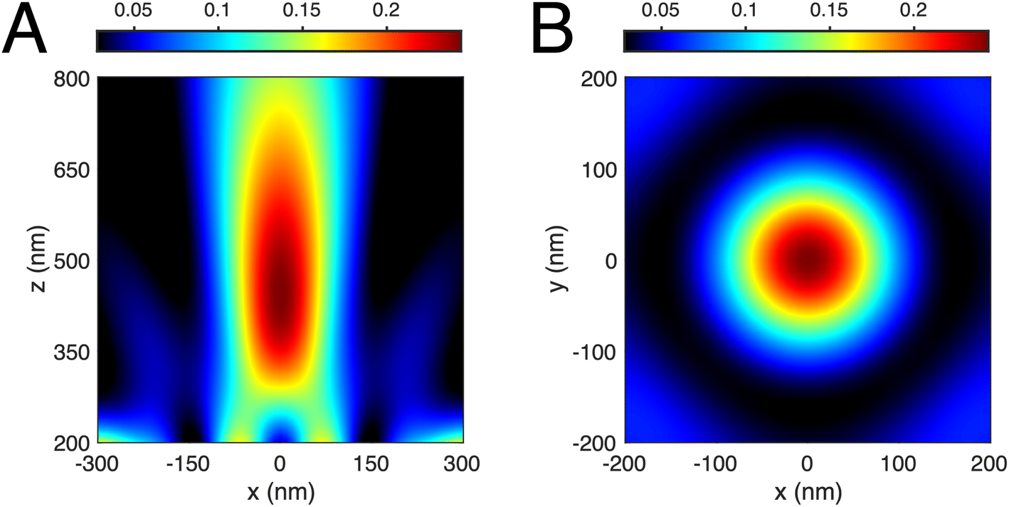 | ||
| Fig. 7 (A) Intensity distribution above the 8-member ring (R = 250 nm) in the plane y = 0. (B) Transverse intensity distribution in the plane z = 450 nm. | ||
This circular array generates a “focus” at z ≈ 450 nm. Although this distance is beyond the near-field, the spot has a lateral width of ≈λ0/4 and an axial extent of ≲λ0. The light intensity drops quickly in every direction, even towards the metal surface, which makes this a potentially useful scheme for microfluidic optical trapping where the trapping volume is away from the wall surface, but still close enough to take advantage of sharper gradients than those obtainable in the far-field and to allow for narrow channels. On the other hand, the separation of the hot spot away from the surface implies that the lithographic scheme of this paper cannot be directly used to image it.
Far-field focusing from surface plasmon lenses fabricated on glass substrates with various nanoscale patterns has been realized experimentally. These patterns have included one-dimensional slit-arrays,24 2D arrays of nanoscale cross-shaped apertures,25 and concentric annular slits.26 The analysis of the optical effects of such structures uses schemes wherein the phase of the emerging surface plasmon waves are matched to the phase of the field radiated from the individual concentric slits or rings to achieve focusing as in a Fresnel lens.24–26 For our structures which are individual cylindrical holes, the same phase-matching scheme could be used to enhance the transmission and focusing of optical power.
Conclusions
In this article we demonstrated an interferometric photolithography approach to accurately map the 3D intensity distributions from various arrangements of circular apertures in a metal films. The method provides a high throughput approach that could assist in the design of nanophotonic/plasmonic devices for various applications. This approach complements numerical simulations that might not easily account for real-world imperfections in materials' composition and morphology. For illustration, we compared two metal films which have different permittivities, and as a consequence produce different optical responses. The method should be useful for validating the design of devices for nano-focusing and for developing integrated plasmon-assisted optical manipulation on a sub-microscopic scale.Conflicts of interest
There are no conflicts of interest to declare.Acknowledgements
This work was partly supported by awards NSF CHE-2107664 and ARO W911NF2010072 (to B. D.), and by NIH R35 GM141922, NIH R01 GM129354, and NSF CHE-0923064 (to S. C. J.). The authors thank the Indiana University Nanoscale Characterization Facility for use of its instruments.References
- N. C. Lindquist, P. Nagpal, A. Lesuffleur, D. J. Norris and S. H. Oh, Three-dimensional plasmonic nanofocusing, Nano Lett., 2010, 10, 1369–1373 CrossRef CAS PubMed.
- D. K. Gramotnev and S. I. Bozhevolnyi, Nanofocusing of electromagnetic radiation, Nat. Photonics, 2014, 8, 13–22 CrossRef CAS.
- H. H. Sheinfux, Y. Lumer, G. Ankonina, A. Z. Genack, G. Bartal and M. Segev, Observation of Anderson localization in disordered nanophotonic structures, Science, 2017, 356, 953–956 CrossRef CAS PubMed.
- K. Wang, E. Schonbrun and K. B. Crozier, Propulsion of gold nanoparticles with surface plasmon polaritons: Evidence of enhanced optical force from near-field coupling between gold particle and gold film, Nano Lett., 2009, 9, 2623–2629 CrossRef CAS PubMed.
- L. Liu, S. Kheifets, V. Ginis, A. Di Donato and F. Capasso, Elliptical orbits of microspheres in an evanescent field, Proc. Natl. Acad. Sci., 2017, 114, 11087–11091 CrossRef CAS.
- M. Laroche, R. Carminati and J.-J. Greffet, Near-field thermophotovoltaic energy conversion, J. Appl. Phys., 2006, 100, 063704 CrossRef.
- J. Aizenberg, J. A. Rogers, K. E. Paul and G. M. Whitesides, Imaging the irradiance distribution in the optical near field, Appl. Phys. Lett., 1997, 71, 3773–3775 CrossRef CAS.
- J. Aizenberg, J. A. Rogers, K. E. Paul and G. M. Whitesides, Imaging profiles of light intensity in the near field: applications to phase-shift photolithography, Appl. Opt., 1998, 37, 2145–2152 CrossRef CAS PubMed.
- D. Amarie, N. D. Rawlinson, W. L. Schaich, B. Dragnea and S. C. Jacobson, Three-dimensional mapping of the light intensity transmitted through nanoapertures, Nano Lett., 2005, 5, 1227–1230 CrossRef CAS.
- C. Deeb, R. Bachelot, J. Plain, A.-L. Baudrion, S. Jradi, A. Bouhelier, O. Soppera, P. K. Jain, L. Huang, C. Ecoffet, L. Balan and P. Royer, Quantitative Analysis of Localized Surface Plasmons Based on Molecular Probing, ACS Nano, 2010, 4, 4579–4586 CrossRef CAS PubMed.
- G. Liang, C. Wang, Z. Zhao, Y. Wang, N. Yao, P. Gao, Y. Luo, G. Gao, Q. Zhao and X. Luo, Squeezing Bulk Plasmon Polaritons through Hyperbolic Metamaterials for Large Area Deep Subwavelength Interference Lithography, Adv. Opt. Mater., 2015, 3, 1248–1256 CrossRef CAS.
- W. Kong, Y. Luo, C. Zhao, L. Liu, P. Gao, M. Pu, C. Wang and X. Luo, Plasmonic Interference Lithography for Low-Cost Fabrication of Dense Lines with Sub-50 nm Half-Pitch, ACS Appl. Nano Mater., 2019, 2, 489–496 CrossRef CAS.
- S. Yu, J. Lu, V. Ginis, S. Kheifets, S. W. D. Lim, M. Qiu, T. Gu, J. Hu and F. Capasso, On-chip optical tweezers based on freeform optics, Optica, 2021, 8, 409–414 CrossRef.
- A. Taflove and S. C. Hagness, Computational electrodynamics: the finite-difference time-domain method, Artech House, Boston, MA, 3rd edn, 2005 Search PubMed.
- Technical Data Sheet – SU-8 Permanent Negative Epoxy Photoresist, https://www.kayakuAM.com Search PubMed.
- E. D. Palik, Handbook of Optical Constants of Solids, Academic Press, Boston, 1998 Search PubMed.
- I. Dika, F. Diot, V. Bardinal, J.-P. Malval, C. Ecoffet, A. Bruyant, D. Barat, B. Reig, J.-B. Doucet, T. Camps and O. Soppera, Near infrared photopolymer for micro-optics applications, J. Polym. Sci., 2020, 58, 1796–1809 CrossRef CAS.
- J. T. Fourkas, Nanoscale Photolithography with Visible Light, J. Phys. Chem. Lett., 2010, 1, 1221–1227 CrossRef CAS.
- H. A. Bethe, Theory of Diffraction by Small Holes, Phys. Rev., 1944, 66, 163–182 CrossRef.
- C. J. Bouwkamp, On Bethe's theory of diffraction by small holes, Philips Res. Rep., 1950, 5, 321–332 Search PubMed.
- T. W. Ebbesen, H. J. Lezec, H. F. Ghaemi, T. Thio and P. A. Wolff, Extraordinary optical transmission through sub-wavelength hole arrays, Nature, 1998, 391, 667–669 CrossRef CAS.
- T. L. Tan, D. Wong, P. Lee, R. S. Rawat, S. Springham and A. Patran, Characterization of chemically amplified resist for X-ray lithography by Fourier transform infrared spectroscopy, Thin Solid Films, 2006, 504, 113–116 CrossRef CAS.
- K. B. Crozier, Quo vadis, plasmonic optical tweezers?, Light: Sci. Appl., 2019, 8, 35 CrossRef.
- L. Verslegers, P. B. Catrysse, Z. Yu, J. S. White, E. S. Barnard, M. L. Brongersma and S. Fan, Planar Lenses Based on Nanoscale Slit Arrays in a Metallic Film, Nano Lett., 2009, 9, 235–238 CrossRef CAS PubMed.
- L. Lin, X. M. Goh, L. P. McGuinness and A. Roberts, Plasmonic lenses formed by two-dimensional nanometric cross-shaped aperture arrays for Fresnel-region focusing, Nano Lett., 2010, 10, 1936–1940 CrossRef CAS PubMed.
- Y. Liu, H. Xu, F. Stief, N. Zhitenev and M. Yu, Far-field superfocusing with an optical fiber based surface plasmonic lens made of nanoscale concentric annular slits, Opt. Express, 2011, 19, 20233–20243 CrossRef PubMed.
Footnote |
| † Electronic supplementary information (ESI) available. See DOI: https://doi.org/10.1039/d2na00570k |
| This journal is © The Royal Society of Chemistry 2023 |